HAL Id: hal-03012184
https://hal.laas.fr/hal-03012184
Submitted on 18 Nov 2020
HAL is a multi-disciplinary open access
archive for the deposit and dissemination of
sci-entific research documents, whether they are
pub-lished or not. The documents may come from
teaching and research institutions in France or
abroad, or from public or private research centers.
L’archive ouverte pluridisciplinaire HAL, est
destinée au dépôt et à la diffusion de documents
scientifiques de niveau recherche, publiés ou non,
émanant des établissements d’enseignement et de
recherche français ou étrangers, des laboratoires
publics ou privés.
Towards MIR VCSELs operating in CW at RT
Daniel Andres Diaz Thomas, Oleksandr Stepanenko, Michaël Bahriz,
Stéphane Calvez, Thomas Batte, Cyril Paranthoen, Eric Tournié, Alexei
Baranov, Guilhem Almuneau, Christophe Levallois, et al.
To cite this version:
Daniel Andres Diaz Thomas, Oleksandr Stepanenko, Michaël Bahriz, Stéphane Calvez, Thomas Batte,
et al.. Towards MIR VCSELs operating in CW at RT. 2019 Compound Semiconductor Week (CSW),
May 2019, Nara, Japan. 2p., �10.1109/iciprm.2019.8819164�. �hal-03012184�
Towards MIR VCSELs operating in CW at RT
D. A. Díaz-Thomas
1, O. Stepanenko
2, M. Bahriz
1, S. Calvez
2, T. Batte
3, C. Paranthoen
3, E. Tournié
1,
A. Baranov
1, G. Almuneau
2, C. Levallois
3and L. Cerutti
1.
1IES, Univ. Montpellier, CNRS, 34000 Montpellier, France2CNRS, LAAS, 7 Avenue du Colonel Roche, F-31400 Toulouse, France3Univ Rennes, INSA Rennes, CNRS,
Institut FOTON – UMR 6082, F-35000 Rennes, France [email protected], [email protected]
Abstract—We present a new design of a Vertical Cavity Surface Emitting Laser (VCSEL) emitting in the Mid Infrared
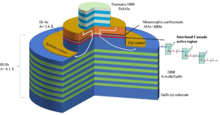
(MIR) spectral range. This new design relies on three key elements: An Interband Cascade (IC) active region, a hybrid structure with a dielectric and a semiconductor Bragg mirror and an arsenide layer for the optical and electric confinement (Fig. 1).
Keywords—VCSEL; ICL; Mid-Infrared
Vertical cavity surface emitting lasers (VCSELs) are particularly well suited for Tunable Diode Laser Spectroscopy due to their intrinsic characteristics. Indeed, the low threshold single frequency emission producing a circular low divergence output beam is beneficial for the development of compact and low power consumption systems for gas spectroscopy. However, in the 3-4 µm range, which encompasses strong absorption bands of many species, only few VCSELs operating either at room temperature (RT) in pulsed mode [1] or in continuous wave (CW) at low temperature [2] have been reported so far. To demonstrate VCSEL operating in the CW regime above RT, we propose a new alternative. This approach is based on Interband Cascade (IC) design for the active region, an arsenide oxide lateral confinement schema, a hybrid-mirror technology and on an intracavity contact (Fig. 1). To provide efficient emission in the 3-4 µm range, the active region is based on a Sb-based IC type-II “W” QW structure. Principal characteristics of Sb-based QW lasers, such as the emission wavelength and threshold, are strongly affected by the growth temperature of the layers located above the active region. We studied a set of edge emitting ICLs designed to operate at 3.3 µm. The lasers were fabricated by Molecular Beam Epitaxy (MBE) on GaSb substrates and their AlGaAsSb top cladding layers were grown at different temperatures. When the growth temperature of the top cladding layer is higher than the optimal one which is used for the active region (435°C), a significant increase of the threshold current densities is observed while the emission wavelength is blue-shifted. This performance degradation is attributed to the inter-diffusion occurring in the active region during the growth. Indeed, it broadens the interfaces and leads to the shift of the quantum level to higher energy, affecting the injection efficiency. Using the optimized growth conditions, we succeeded to fabricate lasers emitting at 3.3 µm and operating in the CW regime up to 80°C (Fig. 2), which confirms the potential of the developed active region. Since the DBRs thickness scales with the wavelength, a fully monolithic approach is not viable in this wavelength range. For this reason, we employed a hybrid VCSEL configuration with a semiconductor AlAsSb/GaSb DBR in the bottom part of the device and a dielectric DBR on the top. Another issue in the VCSEL design is the high electrical resistance of the AlAsSb/GaSb DBR resulting in the overheating of the device. To reduce the ohmic losses we employed an intracavity injection scheme, to avoid highly doped n-type DBRs (in our case ND~5x10¹⁶
cm-3) and thus reach low optical losses in the VCSEL cavity. The top dielectric DBR is composed of Ge and ZnS
and benefits from a large refractive index contrast (n~2) and thus from a wide stop-band. The Fig. 3 presents both reflectivity spectra of a 24 pairs n- doped AlAsSb/GaSb grown by MBE and a 5 pairs Ge/ZnS DBRs deposited
by magnetron sputtering. The two DBRs are well centered at 3.3 µm.
Finally, to ensure an efficient lateral electro-optical confinement, we propose to use an oxide-aperture similarly as short infrared VCSELs [3]. This approach is based on the metamorphic growth and the selective thermal oxidation of an Al(Ga)As heterostructure on top of a GaSb-based half-VCSEL (Fig. 1). This architecture presents several advantages, and in particular the use of the well-controlled Al(Ga)As oxidation process [4].
As already discussed, the growth temperature above the active region affects strongly the performances of the active region. For this reason, we have first determined, with Hall measurement, that n-type GaAs grown at 435°C on undoped GaAs substrate present a better doping efficiency by using Te instead of the usual Si. This is related to the lower activation energy required with Te. Metamorphic GaAs on GaSb growth will be then realized and carefully studied to determine the electrical and optical properties of such layers.
We will show our last achievements towards the realization of MIR-VCSELs.
This work was partially supported by the French "Investment for the Future" program (EquipEx EXTRA, ANR-11-EQPX-0016) and by the French ANR (MIMIC-SEL, ANR-16-CE24-0011). It partially benefited from support of the French RENATECH network and its LAAS technological facility.
[1] W.W. Bewley et al., Appl. Phys. Lett., 109, 15108 (2016) [2] G.K. Veerabathran et al., Appl. Phys. Lett., 110, 071104 (2017) [3] Y. Laaroussi et al., Electron. Lett., 48, (2012)
Fig 1. Scheme of the MIR VCSEL with interband cascade active region, a metamorphic oxide lateral confinement and a hybrid-mirror technology.
Fig. 2: I-P-V characteristics of narrow ridge device operating in cw-mode. Inset: laser spectrum at 30°C under 150 mA CW current injection.