UNIVERSITÉ DE MONTRÉAL
IMPLEMENTATION OF DATA-DRIVEN APPLICATIONS ON TWO-LEVEL RECONFIGURABLE HARDWARE
HIMAN KHANZADI
DÉPARTEMENT DE GÉNIE ÉLECTRIQUE ÉCOLE POLYTECHNIQUE DE MONTRÉAL
MÉMOIRE PRÉSENTÉ EN VUE DE L’OBTENTION DU DIPLÔME DE MAÎTRISE ÈS SCIENCES APPLIQUÉES
GÉNIE ÉLECTRIQUE AOÛT 2016
UNIVERSITÉ DE MONTRÉAL
ÉCOLE POLYTECHNIQUE DE MONTRÉAL
Ce mémoire intitulé :
présenté par : KHANZADI Himan
en vue de l’obtention du diplôme de : Maîtrise ès sciences appliquées a été dûment accepté par le jury d’examen constitué de :
M. BRAULT Jean-Jules, Ph. D., président
M. DAVID Jean-Pierre, Ph. D., membre et directeur de recherche M. SAVARIA Yvon, Ph. D., membre et codirecteur de recherche M. BOIS Guy, Ph. D., membre
RÉSUMÉ
Les architectures reconfigurables à large grain sont devenues un sujet important de recherche en raison de leur haut potentiel pour accélérer une large gamme d’applications. Ces architectures utilisent la nature parallèle de l’architecture matérielle pour accélérer les calculs. Les architectures reconfigurables à large grain sont en mesure de combler les lacunes existantes entre le FPGA (architecture reconfigurable à grain fin) et le processeur. Elles contrastent généralement avec les Application Specific Integrated Circuits (ASIC) en ce qui concerne la performance (moins bonnes) et la flexibilité (meilleures).
La programmation d’architectures reconfigurables est un défi qui date depuis longtemps et pose plusieurs problèmes. Les programmeurs doivent être avisés des caractéristiques du matériel sur lequel ils travaillent et connaître des langages de description matériels tels que VHDL et Verilog au lieu de langages de programmation séquentielle. L’implémentation d’un algorithme sur FPGA s’avère plus difficile que de le faire sur des CPU ou des GPU. Les implémentations à base de processeurs ont déjà leur chemin de données pré synthétisé et ont besoin uniquement d’un programme pour le contrôler. Par contre, dans un FPGA, le développeur doit créer autant le chemin de données que le contrôleur. Cependant, concevoir une nouvelle architecture pour exploiter efficacement les millions de cellules logiques et les milliers de ressources arithmétiques dédiées qui sont disponibles dans une FPGA est une tâche difficile qui requiert beaucoup de temps. Seulement les spécialistes dans le design de circuits peuvent le faire.
Ce projet est fondé sur un tissu de calcul générique contrôlé par les données qui a été proposé par le professeur J.P David et a déjà été implémenté par un étudiant à la maîtrise M. Allard. Cette architecture est principalement formée de trois composants: l’unité arithmétique et logique partagée (Shared Arithmetic Logic Unit –SALU-), la machine à état pour le jeton des données (Token State Machine –TSM-) et la banque de FIFO (FIFO Bank –FB-). Cette architecture est semblable aux architectures reconfigurables à large grain (Coarse-Grained Reconfigurable
Architecture-CGRAs-), mais contrôlée par les données. En effet, dans cette architecture, les
banques de registres sont remplacées par les FB et les contrôleurs sont les TSM. Les opérations commencent dès que les opérandes sont disponibles dans les FIFOs qui contiennent les
opérandes. Les données sont déplacées de FB à FB à travers les SALU tel que programmé dans la mémoire de configuration du TSM. Les résultats finaux sont sauvegardés dans les FIFOs. Ce projet de recherche se fonde sur les CGRAs et les Overlay Architectures (OEA), qui permettent aux concepteurs de profiter d’une architecture précompilée sur FPGA et encore fournir un moyen de configurer le système à un haut niveau. Nous proposons une méthodologie de conception pour implanter un algorithme sur un FPGA qui est préconfiguré avec un CGRA. L’algorithme de conversion nécessite un graphe de flux de données (DFG) comme entrée qui est typiquement le corps d’une boucle. Une quantité maximale d’opérations est traitée en parallèle et une nouvelle itération de la boucle est lancée le plus tôt possible (ASAP). Idéalement, ce traitement est fait avant que la boucle en exécution ne soit finie. Ceci est réalisé en utilisant des techniques de pipelinage logiciel inspirées de la technique d’ordonnancement itératif de Modulo (Iterative Modulo Scheduling). L’ordonnancement Modulo est modifié de manière à ce que les phases de placement et de routage soient intégrées. Dans l’architecture proposée, un tissu de calcul générique contrôlé par les données est connecté aux processeurs standards. En fait, la nouvelle architecture permet aux développeurs de contrôler, de recueillir et de gérer le flux de données sur les banques FIFO. Le développeur est aussi capable de répartir l’exécution de l’application entre les processeurs Microblaze et le TSM. Pour valider l’architecture et le procédé de conception proposées, nous avons développé un exemple illustratif dans lequel un processeur envoie une image en format RGB au tissu de calcul générique. Dans le tissu, l’image est transformée en format Y, Cr, Cb. Les résultats montrent que, grâce au contrôleur DMA entre la mémoire et le tissu, un gain de vitesse de 50 peut être atteint par rapport à une implémentation logicielle pure.
ABSTRACT
Coarse-grained reconfigurable computing architectures have become an important research topic because of their high potential to accelerate a wide range of applications. These architectures apply the concurrent nature of hardware architecture to accelerate computations. Substantially, coarse-grained reconfigurable computing architectures can fill up existing gaps between FPGAs and processor. They typically contrast with Application Specific Integrated Circuits (ASICs) in connection with performance and flexibility.
Programming reconfigurable computing architectures is a long-standing challenge, and it is yet extremely inconvenient. Programmers must be aware of hardware features and also it is assumed that they have a good knowledge of hardware description languages such as VHDL and Verilog, instead of the sequential programming paradigm. Implementing an algorithm on FPGA is intrinsically more difficult than programming a processor or a GPU. Processor-based implementations “only” require a program to control their pre-synthesized data path, while an FPGA requires that a designer creates a new data path and a new controller for each application. Nevertheless, conceiving an architecture that best exploits the millions of logic cells and the thousands of dedicated arithmetic resources available in an FPGA is a time-consuming challenge that only talented experts in circuit design can handle.
This project is founded on the generic data-driven compute fabric proposed by Prof. J.P. David and implemented by M. Allard, a previous master student. This architecture is composed of three main individual components: the Shared Arithmetic Logic Unit (SALU), the Token State Machine (TSM) and the FIFO Bank (FB). The architecture is somewhat similar to Coarse-Grained Reconfigurable Architectures (CGRAs), but it is data-driven. Indeed, in that architecture, register banks are replaced by FBs and the controllers are TSMs. The operations start as soon as the operands are available in the FIFOs that contain the operands. Data travel from FBs to FBs through the SALU, as programmed in the configuration memory of the TSMs. Final results return in FIFOs. The present work builds on CGRAs, and Overlay Architectures (OAs), that allow a designer to take advantage of a pre-compiled FPGA architecture and still provide a way to configure the system at a higher level. We propose a design methodology to map an algorithm on an FPGA
preconfigured with a CGRA. The mapping algorithm requires a data flow graph (DFG) as input, typically the body of a loop. A maximum number of operations are processed in parallel, and a new iteration of the body loop is started as soon as possible, ideally before the completion of the current one, by using software pipelining techniques, inspired of Iterative Modulo Scheduling. Modulo scheduling is modified in a way that placement and routing phases are integrated to the procedure. In the proposed architecture, a generic data-driven compute fabric is interfaced to standard processors. In fact, the new architecture enables the user to control, collect and manage the data flow on FIFO banks. The programmer is also able to program an application split between Microblaze processors and TSMs. To validate the proposed architecture and design method, an illustrative example is developed in which a processor sends an RGB image to a processing fabric, where it is converted to Y, Cr, Cb. Results show that thanks to DMA between the memory and the fabric, a speedup of 50 are reached compared to a pure software implementation.
TABLE OF CONTENTS
RÉSUMÉ ... III ABSTRACT ... V TABLE OF CONTENTS ...VII LIST OF TABLES ... X LIST OF FIGURES ... XI LIST OF SYMBOLS AND ABBREVIATIONS... XIV LIST OF APPENDICES ... XVI
CHAPTER 1 INTRODUCTION ... 1
CHAPTER 2 STATE-OF-THE-ART ... 6
2.1 Introduction ... 6
2.2 High performance computing architectures ... 7
2.2.1 Central Processor Unit (CPU) ... 7
2.2.2 Graphical Processor Unit (GPU) ... 9
2.2.3 Field Programmable Gate Array (FPGA) ... 10
2.2.4 Coarse-Grained Reconfigurable Architecture (CGRA) ... 11
2.3 Coarse-Grained Reconfigurable Architectures ... 12
2.3.1 Reconfigurable Pipelined Datapath (RaPiD) ... 12
2.3.2 Reconfigurable data path array (rDPA) ... 12
2.3.3 PipeRench ... 12
2.3.4 Reconfigurable Multimedia Array Coprocessor (REMARK) ... 14
2.3.5 Architecture for Dynamically Reconfigurable Embedded System (ADRES) ... 15
2.3.7 A mesh of parallel computing and communicating nodes ... 16
2.4 Programming of most popular CGRAs ... 20
2.4.1 Programming REMARK coprocessor ... 20
2.4.2 Programming MorphoSys coprocessor ... 21
2.4.3 Programming PipeRench Architecture ... 21
2.4.4 Programming RaPiD Architecture ... 22
2.4.5 Different techniques of the mapping applications on the CGRAs ... 22
2.4.6 Modulo Scheduling ... 25
2.4.7 Modulo Scheduling and CGRA ... 26
2.4.8 Summary of CGRA mapping algorithms ... 27
2.5 Conclusion ... 28
CHAPTER 3 PROPOSED SOLUTION BASED ON MODULO SCHEDULING INTEGRATED WITH PLACEMENT AND ROUTING ... 30
3.1 Introduction ... 30
3.2 Mapping Applications on Two-Level Configurable Hardware ... 31
3.2.1 Mapping procedure ... 31
3.2.2 Propose an Assembly Code for Computing Fabric ... 41
3.2.3 Generates the instruction bits for TSMs using WinTim32 Application... 42
3.3 Runtime Executing Applications on Parallel Computing and Communicating Nodes . 43 3.3.1 Modified Fabric: ... 44
3.3.2 Runtime Executing Application on the Computing Fabric ... 46
3.3.3 General View of Runtime Executing Application Hardware ... 54
CHAPTER 4 EXPERIMENTAL RESULT ... 57
4.1 Introduction ... 57
4.2 Simulation and manual mapping application on computing fabric... 58
4.3 Runtime RGB-YCbCr Transform on the CGRA ... 64
4.4 Conclusion ... 68
CHAPTER 5 CONCLUSION AND FUTURE WORK ... 69
CHAPTER 6 FUTURE IMPROVEMENT: ... 71
BIBLIOGRAPHY ... 72
LIST OF TABLES
Table 2-1- properties of programming environment of CGRA. ... 27 Table 2-2-Technology mappings in recent years ... 28 Table 3-1-equivalent assembly code for a simple C code ... 50 Table 3-2- Implemented software decoder to select each FIFOs in one Tile of computing fabric 51 Table 4-1- require clock cycle to perform RGB-YCbCr application (length is 340 *3 R-G-B) .... 67 Table 4-2- Resources Utilizing by computing fabric 2×2 ... 67
LIST OF FIGURES
Figure 1-1- Reconfigurable architecture proposed by Allard et al. [3]© 2010 IEEE. ... 3
Figure 2-1-PipeRench Architecture [24]©2000 IEEE ... 13
Figure 2-2-MorphoSys reconfigurable computing[25] © 2000 IEEE ... 14
Figure 2-3-REMARK Architecture [26] © 1998 IEEE. ... 15
Figure 2-4-EGRA Architecture[29] ©2010 IEEE ... 16
Figure 2-5- CGRA Proposed by Allared [3] © 2010 IEEE ... 17
Figure 2-6-The architecture of the SALU [3] © 2010 IEEE ... 17
Figure 2-7- Schematic of: a) router type1:router1_0 , b) router type 2: router 2_0 [3] © 2010 IEEE ... 18
Figure 2-8-Central Router Network [3] © 2010 IEEE ... 19
Figure 2-9-Block Diagram of a TSM [3] © 2010 IEEE... 20
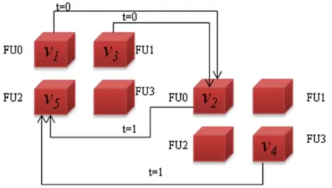
Figure 3-1- Illustrative example input data flow graph loop body ... 32
Figure 3-2- Illustrative example target Hardware Architecture Description ... 32
Figure 3-3- Calculate the Minimum Initiation Interval (MII) ... 33
Figure 3-4- Pseudo code for Hardware Architecture description example ... 34
Figure 3-5- ASAP and ALAP scheduling ... 35
Figure 3-6- create an ordered list of nodes ... 35
Figure 3-7- Main Function of the mapping DFG onto fabric ... 36
Figure 3-8- Modulo Routing Resource Graph (MRRG) for II=2 ... 37
Figure 3-9- Generate MRRG ... 37
Figure 3-10- Modulo Scheduling Place&Route (MSPR) ... 38
Figure 3-12-MSPR result for our illustrative example Corresponding II=2 ... 41
Figure 3-13-Two configurations (left and right) to map our sample DFG ... 42
Figure 3-14- New Network Router. ... 45
Figure 3-15- Merging Data from two routers to a FIFO Bank ... 46
Figure 3-16 - Microblaze coupled with the fabric ... 48
Figure 3-17- Double Link between Microblaze and Fabric for writing and reading process ... 49
Figure 3-18- Single Link communicating between Microblaze and fabric for writing and reading process ... 49
Figure 3-19- A simple example of access to a FIFO by CDMA ... 52
Figure 3-20- a) spread out data by Hardware b) spread out data by the software ... 53
Figure 3-21- Runtime Execution Applications Architecture ... 55
Figure 3-22- Screen shot of the Implemented architecture to support runtime execution of the applications using EDK ... 55
Figure 4-1- RGB-YCbCr DFG application ... 58
Figure 4-2-Target architecture (SALU00, SALU01, and their FBs only) ... 59
Figure 4-3- MRRG of the target architecture composed of two SALU ... 59
Figure 4-4-MSPR of Y output of RGB-YcbCr DFG application (II=0). ... 61
Figure 4-5- Final configuration context ... 61
Figure 4-6- Simulation Result Based given configuration context for RGB-YCbCr application . 62 Figure 4-7- DFG of a 4-point FFT ... 63
Figure 4-8-MSPR of a 4-Point FFT (II=2) ... 63
Figure 4-9-FFT 4-point Simulation (II=2) ... 64
Figure 4-11- Capturing data transfer by the chip scope ... 66 Figure 4-12- Eight words transferring By DMA to fabric ... 66
LIST OF SYMBOLS AND ABBREVIATIONS
ALU Architecture Logic Unit
ADRES Architecture for Dynamically Reconfigurable Embedded system CC Configuration Context
CU Control Unit
CDFG Control Dataflow Graph CDMA Central Direct Memory Access CPU Central Processing Units
CGRA Coarse-Grained Reconfigurable Architecture
CP Critical Path
DIL Dataflow Intermediate Language DFG Data Flow Graph
EGRA Expression-Grained Reconfigurable Array EMS Edge-centric Modulo Scheduling
FGRA Fine-Grained Reconfigurable Architecture
FU Function Unit
FB FIFO Bank
FPGA Field-Programmable Gate Arrays GPU Graphics Processing Units HPC High Performance Computing II Initiation Interval
ILP Integer Linear Programming LUT Lookup Table
LLP Loop Level Parallelism
MRRG Modulo Routing Resource Graph MSPR Modulo Schedule Place & Route MII Minimum Initiation Interval
MS Modulo Scheduling
OpenCL Open Computing Language PE Processing Element
QEA Quantum-inspired Evolutionary Algorithm RAC Reconfigurable ALU Cluster
RCA Reconfigurable Computing Architecture RC Reconfigurable Cell
RaPiD Reconfigurable Pipelined Datapath rALU reconfigurable ALU
rDPA Reconfigurable Data Path Array
REMARC Reconfigurable Multi Media Array Coprocessor
RF Register File
RISC Reduce Instruction Set Computing SOC System on Chip
SALU Shared-ALU
TSM Token State Machine
SA Simulated Annealing
LIST OF APPENDICES
APPENDIX A – ASSEMBLY CODES FOR PROPOSED ARCHITECTURE ... 80 APPENDIX B – WINTIM32 ... 89
CHAPTER 1
INTRODUCTION
Having billions of transistors on a single chip, the best way to design modern computing chips is to make it more parallel and configurable. General purpose processors have evolved to multicore chips, where each core is independent of the other cores, but shares memory resources. For example, the Xeon PHI 7120A processor has 61 embedded cores running up to 244 threads in parallel at 1.2GHz[1].
Graphics Processing Units (GPUs) offer thousands of cores running in parallel. However, to be more efficient, the same instruction must be applied to multiple data, i.e. single instruction, multiple data (SIMD) architecture. For example, the Nvidia K40 chip has 2880 cores leading to a peak performance of 4.3 TFLOPS for single precision arithmetic[2].
Both general purpose processors and GPUs are highly configurable devices, since they are founded based on the Von Neuman model. They benefit from more than 50 years of research and development in programming languages, libraries, and design tools, enabling computer scientists to rapidly design and prototype complex applications.
However, mainstream processors are not necessarily the best targets for algorithms with high data dependencies and/or low latency constraints, since the applications must be transformed to fit the hardware. In such context, the best performances are achieved when the hardware is tailored to the algorithm, as with Application Specific Integrated Circuits (ASICs) or Field Programmable Gate Arrays (FPGAs). It is known that designing a complex chip is a long task reserved for experts in the field. Despite decades of research and development, which today enable some high-level circuit design, the need for experts and the long development times are presently the biggest obstacles to the use of FPGAs as mainstream processing devices.
Coarse Grain Reconfigurable Architectures (CGRA) are intermediate solutions between mainstream processors and FPGAs. They are consisted of several units for the processing and exchanging of data with their neighbor units, which are typically organized as a mesh at very low level. Each unit can be programmed to implement a part of the application and route the data to other units. Thus, it is possible to tailor the hardware to the application, without the help of a hardware design specialist. CGRAs are good candidates for repetitive computations with high data
dependency. They are employed as coprocessors to accelerate loops and to let the main processor calculate control-dominant parts of an application.
Although the architecture proposed by Allard et al. [3] (refer to pages 35-38 ) is similar to CGRAs, it is based on a data-driven mode of operation, i.e., the register banks are replaced with FIFO Banks (FBs) and the controllers are Token State Machines (TSMs). Thus, the operations start as soon as the operands are available in the FIFOs that contain the operands. The main advantage of this architecture [3] is that it results in a fast and simple implementation of a user-defined design implemented over a reconfigurable computing architecture.
On the other hand, the available hardware resources increase with each new generation of complex hardware designs and designers should have access to these resources. To this end, designers require a strong knowledge of the hardware design.
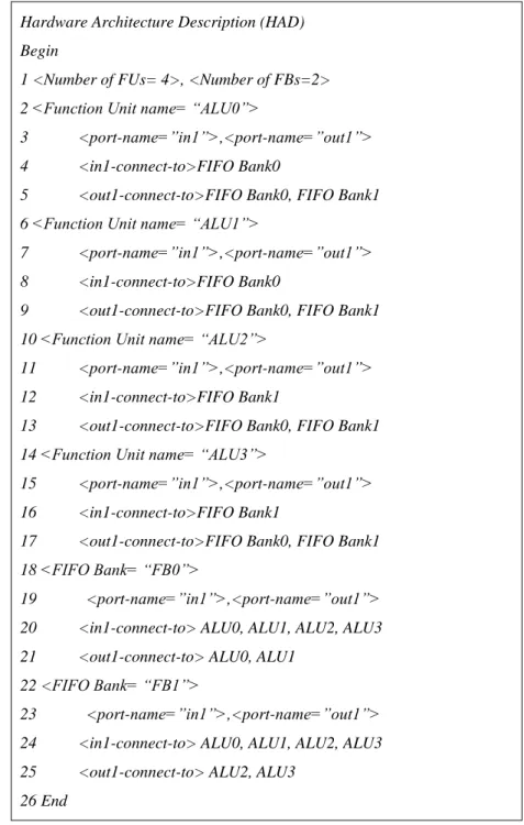
In fact, Allard’s architecture aims at effectively exploiting increasingly abundant resources to increase the performance of hardware. The improved performance is achieved by using dedicated hardware resources with the simplicity and flexibility of software development. Also, Allard et. al[3] introduced the concept of two different configuration levels. At the lowest level, a hardware design specialist assembles a dedicated CGRA, which is composed of building blocks, such as token-based ALUs, FIFOs, and sequences, i.e., the control path of a token machine. The circuit is then synthesized, placed and routed on an FPGA. At the highest level, computer scientists may program the token machines to implement an application. Thus, the architecture may offer many advantages, including reconfigurability, evolution, high (and low) level programming, and low-level parallelism exploitation.
Figure 1-1 shows the architecture proposed by [3]. As can be seen in this figure, the architecture includes three components: Shared-ALU (SALU), FBs and TSM. The architecture can be extended in both dimensions. All the computing and routing capabilities of the fabric are concentrated in the SALU, which is consisted of eight independent ALUs, their associated decoder, and one central router network. The decoders are used to establish connections between the FBs and ALUs to handle the token production-consumption. In addition, they send data tokens to the ALUs and get
back the results. Each decoder has two internal buffers (local accumulators) to temporarily store operands.
Each ALU is controlled by its programmable TSM. TSMs contain the instructions, which include the address of the operands (local accumulator or FB), the type of operation (16 different arithmetic and logic operations are supported) and the address of the result that could be located in any of the FBs connected to the SALU or in a local accumulator.
Figure 1-1- Reconfigurable architecture proposed by Allard et al. [3]© 2010 IEEE.
However, the proposed CGRA has been elaborated with fixed applications and was not directly capable of supporting advanced features, such as running the application with new data at runtime. It is to be noted that the FIFO’s contents are charged once the architecture is synthesized. If the FIFOs need to be filled up with a new data, the CGRA should be re-synthesized. Given this, the application of the proposed CGRA is restricted to executing a few input data in parallel. In addition, at the highest level, this architecture still requires an auxiliary method to take advantage of the simplicity and flexibility of software development. In fact, mapping an application manually with thousand operations on the CGRA was essentially an intractable process.
Due to the abovementioned challenges, this work intends to address the problem of mapping complex applications in the Allard et al. architecture.
At a high level, mapping a complex data flow graph with hundreds or thousands of nodes onto the Allard et al. architecture is a complex, tedious and error-prone task. This work proposes an algorithm to automate such mapping. Furthermore, the CGRA is enhanced regarding supporting runtime executing applications. The proposed architecture is consisted of Allard et al. architecture (CGRA-based) that is tightly coupled with a processor-based IP (Microblaze).
In the proposed architecture, CGRA is defined as a custom peripheral Intellectual Properties (IP). This IP is attached to the Processor Local Bus (PLB), where the Microblaze is defined as a microprocessor. To run the applications with a high data throughput, a Central Direct Memory Access (CDMA) is employed. Using the CDMA, the CGRA’s FIFO banks could dynamically be recharged with new data tokens. Then, it leads to support runtime execution applications through CDMA by recharging embedded FIFO banks inside the CGRA.
The new architecture makes it possible to analyze the application code to separate the non-critical from sequential or controller application code. The users of this architecture will be able to determine what section of the application should be executed on the CGRA and the Microblaze. The loops are executed on the CGRA as computation-intensive kernels while the Microblaze can execute the sequential code.
In fact, the new architecture enables the user to control, assemble and manage the data flow on FIFO banks. The programmer is also able to program both Microblaze processors and Token State Machines. The proposed architecture provides a simple and fast method for programmers enabling the runtime execution of the applications on the hardware at high abstraction level implemented through software.
The contributions of this work can be summarized as:
Introducing an automated mapping of the application on proposed CGRA to facilitate the implementation of algorithms that are executing over that CGRA.
Proposing a reconfigurable architecture model to manage, control and collect data tokens set to the CGRA through a high-level language (C/C++) supported by software (Software Development Kit (SDK)). These modifications on data tokens executing over the hardware
are possible at run time without a need to repeat synthesizing, placing and routing. Ease-of-use and flexibility of the proposed architecture provide an opportunity to support applications requiring dynamic adaptation.
This work is organized as follows: in Chapter 2, a literature review is done to clearly identify the subject and describe exiting mapping algorithms in reconfigurable architectures based on CGRA as well as describing the architecture proposed by Allard et al. In Chapter 3, a solution to automate the mapping of applications on the CGRA is proposed in detail . In addition, a new architecture is explained in detail to support runtime applications on existing CGRA.
In Chapter 4, experimental results are presented. Fast Fourier Transformation (FFT) and matrix multiplication applications showed that the proposed automated methodology could lead to high throughput and/or low latency within a reasonable design time. The proposed architecture was elaborated, synthesized, placed and routed on a Xilinx Virtex-5 FPGA using suitable tools. In addition, the runtime matrix multiplication result showed that the proposed architecture could lead to a high throughput.
CHAPTER 2
STATE-OF-THE-ART
2.1 Introduction
The demand for high-speed accelerator devices or computing architectures to perform a computation has significantly risen regarding. High-Performance Computing (HPC) architectures is a suitable choice to address the demands mentioned above. HPC is used to solve complex science problems that need high bandwidth, low latency, and high computing capabilities.
ASIC and DSP processors are built based on dedicated hardware that have been established in this market. The demand for applications that could handle large real-time data streams creates new demands, such as having general purpose microprocessors and more powerful FPGAs. However, programming the FPGAs is not an easy task, since the programmer must have strong knowledge on low-level design using low-level languages, such as VHDL and Verilog. The high-level synthesis is an automated design process to generate a register-transfer level design from an algorithmic description of a desired behaviour. Therefore, high-level synthesis facilitates the programming of the digital systems, such as FPGAs. The high-level synthesis includes three important tasks that are scheduling, allocation, and binding to form the complete control data path and implement it onto the hardware. Scheduling determines the cycle that an operation can be executed. The most famous scheduling algorithm are: list scheduling (ASAP, ALAP), force-directed, time and resource constrained scheduling, and integer linear programming. The Allocation process determines the appropriate number of the processing unit, storage, and interconnection units. Finally, the binding connects placed and scheduled operations according to their data dependencies. Walker et.al[4] introduced a tutorial for the scheduling problem which is used by the high-level synthesis concept.
In this section, we will first describe the mainstream processors for high-performance computing architectures, such as CPU, GPUs, FPGAs, and CGRA. The most popular CGRAs, such as Rapid, rDPA, PipeRench, MorphoSys, REMARK, ADRES, EGRA, and a mesh of parallel computing and communicating nodes are then studied. We will also present the available programming methods
to compile REMARK, MorphoSys, PipeRench and RaPiD architectures and explain the state-of-the-art methods in mapping applications on the CGRAs.
Modulo scheduling problem will be addressed in the following section as the most popular method in mapping application onto CGRAs. Finally, the summarized mapping applications onto CGRAs will be presented in two different tables at the end of this section.
2.2 High performance computing architectures
Hardware technologies are very important since they accelerate HPC applications. Based on the quest of HPC, the following components are used as HPC hardware: (i) central processing units (CPUs) that are taking multiple processor cores into account for parallel computing; (ii) graphics processing units (GPUs) that process huge data blocks in parallel ; (iii) Hybrid CPUs/GPUs computing that is a very common solution for supercomputers, as well as its capability for desktop computers and (iv) Field-Programmable Gate Arrays (FPGAs) that are also very useful for a certain class of demanding applications.
Rapid growth and development of complex computation require high-performance computing (HPC) hardware. HPC is used in parallel processing techniques to solve complex engineering problems needing high bandwidth, high computing capability and low latency. Because of this growth, it is impossible to reach high-performance computing by traditional computing systems that contain only one CPU. To reach to higher performance, the HPC utilizes a combination of different hardware platforms such as CPUs, GPUs and FPGA[5], [6] that will be discussed in the following.
2.2.1 Central Processor Unit (CPU)
CPU is a vital part of a computer and contains two essential components, ALUs and Control Units (CUs). The ALU manages the arithmetic and logical operations, whereas CUs can access to the memory to read and execute the instructions[7], [8]. The design of CPU is based on the prefetching and pipelining architecture. A computer architecture that uses this method facilitates fetching the instruction before the current instruction ends and consequently, the throughput of instructions
increases. In order to decrease the required time to execute a program and to improve the high-performance computers, the Reduced Instruction Set Computer (RISC) is used in CPU design. Utilizing RISC may increase the number of internal registers inside the CPU in a way that the data flow pipelining will be improved [7]. A brief history of CPU progress is studied in the following. The first microprocessor was emerged by Intel, 4-bit 4000, in 1970. This chip contained 2,300 transistors with the capability of executing 92,000 instructions per second[8], [9]. Shortly, Intel came with new innovations in CPU evolution in 8008 and 8080. Over time, the new evolution of CPU is continually developed, and others companies, such as AMD and Motorola introduced their products as a competitor to Intel. In 1993, one of the most popular CPUs called “Pentium” was introduced with 60 MHz clock frequency and 100 millions of instructions per second. The evolution on the Pentium continued until 2008, and both Intel and AMD introduced new generation models of CPU. Intel has developed its product and introduced the first CPU, which had 2 billion transistors [7]–[9].
According to Moore’s law, the number of transistors that could be placed inside a chip is restricted and is approximately doubled every two years. However, available single core CPU may not respond to new applications, since they require to be operated at high speed with higher performance without lowering the price. Therefore, the competition of producing CPUs operating at higher frequencies and high performance inside one core has reached a plateau.
The computer architects reached a new approach in order to have better performance; moving the technology towards the multicore instead of using only one core inside a chip. A multicore processor often runs in slower frequencies than one single core, but with an increased calculation throughput. The term “multicore” refers to an integrated processor including two or more processors attached in order to increase the performance via parallel processing. In parallel processing, many calculations are performed at the same time and thus, the large problems can be solved by breaking them into several smaller parts and executing each concurrently[7]–[9]. The multicore processor can execute multiple instructions at the same time in order to increase the speed by high parallel computing algorithms implemented in software. With the use of parallel computing, large problems may be solved faster.
In the following paragraph, the available multicore processors by Intel, AMD and Tilera will be discussed. AMD Opteron 6000 series processors are based on multicore processors (containing 4, 8, 12, and 16). These series of processors support quad-channel memories in order to achieve high bandwidth amount to 51.2 GB/s [6], [10]. The Tilera family processors contain 16 to 100 cores based on Tilera’s iMesh on-chip network that are optimized for networking, video and cloud applications. Each core consists of 64-bits very long instruction level. The mesh interconnection technology used in Tilera is based on two modules. First module is used for streaming applications and the second module in memory communication to reach high performance shared memory[11]. The first high-performance architecture of Intel was introduced by Xeon E5 family that supports up to 8 cores with 20 MB shared memory[1]. They have also developed high-performance computing and introduced a new Xeon family. This new generation of Intel is based on multicore processors that extract a good performance from high parallel computing called Intel Xeon Phi, which is based on Intel Many Integrated Core architecture. Intel Xeon Phi coprocessors are PCI Express cards that enable higher performance gains for parallel tasks. Intel Xeon Phi coprocessors provide up to 61 cores, 244 threads and 1.2 teraflops (Floating Point Operations per Second).These coprocessors are categorized within three main product families; Intel Xeon Phi coprocessor 3100, Intel Xeon Phi coprocessor 5100, and Intel Xeon Phi coprocessor 7100.
2.2.2 Graphical Processor Unit (GPU)
GPU has recently become an influential coprocessor as a general purpose processor. GPUs are more efficient to perform parallel processing than CPU. This superiority is due to the basic nature of the GPU based on parallel data architecture and programmable technology[6][12]. GPUs are designed to accelerate demonstration and processing of visual images on a graphical output device. GPUs can process and display millions of pixels, simultaneously, and their design objective was to assist the video processing on devices, such as personal computers, cell phones, , etc.[7]. Design architects employ the natural properties of GPU to solve the complex scientific problems via general purpose processors. The general purpose GPUs are currently used in various HPC application domains such as medical imaging, bioinformatics, and embedded systems and are an ideal option for accelerator devices for massive data-parallel processing [12].
The programming model of GPU is based on a scalable processing array that consists of single instruction multiple threads having several stream processors. There are several memory spaces in GPUs, such as global and local memory. The global memory is accessible by all cores, and local or shared memory is related to each microprocessor[13]. The 1990's years were the beginning of GPUs by the introduction of 86C911 card by S3, which was one of the first standards for the GPU industry. Evolution of GPUs continued to two-dimensional graphics processing in 1990's up to 3D processing graphics processing, which are used in lower-end laptops today[8]. AMD and NVIDIA introduced several models of GPUs, and each one has specifically improved characteristics compared to the previous versions. The newly developed model of GPU called Tesla K80 that was introduced by NVIDIA and comprised 24 GB memory and up to 2.91 TFLOPS double precision performance with 480GB/s bandwidth. In fact, it consists of two GPUs placed inside one packet, where each GPU has 2496 cores [14]. Tesla K80 is ideal for high-performance computing accelerator that requires massive data throughput in single and double precision mode. AMD designed AMD FirePro S10000, and it has 3584 stream cores with the accuracy of 1.48 TFLOPS of double precision or 5.91 TFLOPS of single precision[14].
2.2.3 Field Programmable Gate Array (FPGA)
FPGAs are reconfigurable integrated systems and are semiconductor devices consisted of many logic blocks linking together through programmable routing networking, embedded memory block, and digital signal processing blocks. The logic block is the main component of FPGAs that is implemented in a Lookup Table. LUTs contain a small attached memory that is programmed for the output logic based on the inputs. FPGAs’ resources can be configured and linked together in order to create custom instruction pipeline to determine which data is processed. On the other hand, in CPU and GPU topologies the data path are fixed [8], [15].
FPGA is highly based on high-level parallelism and is a perfect choice for implementing a portion of the application that requires extensive parallelism. Xilinx and Altera are two well-known companies to develop FPGAs. Stratix 10 is the newest FPGA introduced by Altera. Stratix 10 device architecture was manufactured on the Intel 14 nm Tri-Gate technology that provides the highest performance and more power efficiency. Stratix 10 SX SoCs hard processor system with
64 bit quad-core ARM Cortex-A53 processor. The debug tools and heterogeneous advanced languages such as OpenCL developed by Altera SDK as design environment facilitate the application implementation on FPGA [16].
Xilinx Ultra Scale architecture is another high accelerator unique device that provides high-performance, high-bandwidth and low latency. It should be noted that the ultra-scale devices are suitable for processing massive data flows, since they have high bandwidth and low latency [17].
2.2.4 Coarse-Grained Reconfigurable Architecture (CGRA)
Based on granularity, reconfigurable computing architecture can be divided into two categories: fine-grained and Coarse-Grained Reconfigurable Architectures [18], [19].
CGRAs are indicated as application-specific reconfigurable devices or embedded FPGAs. CGRAs are introduced to tackle the disadvantage of Fine-Grained Reconfigurable Architectures (FGRAs) for computing application. Some disadvantages of FGRAs are the configuration time, routability and logic granularity. Logic granularity means that the architecture for FGRA is based on logic elements and is not suitable to handle complex signal processing and multimedia computations. The reconfiguration of FGRA is performed at bit-level; therefore the logic blocks are required to operate wide data path, and its routing path may have a huge wide range and poor routability. CGRA operates at the multiple-bit level. Therefore, it has less configuration time than FGRA [20], [21].
CGRAs are consisted of an array of FUs interconnected by a mesh topology network and register files are scattered among the CGRA. Some key characteristics of CGRAs include size, node functionality, topology, and register file sharing. The size refers to the number of FUs that can vary (e.g. 64 FUs); they are arranged as an array of 8×8. The functionality of each FU can be determined to execute an arithmetic or logic operation, such as addition, subtraction or multiplication. There are several configuration networks topology to provide interconnection between FUs. For example, each node can be connected to its four orthogonal or eight diagonal neighbors. CGRAs can include a local memory. The FUs have access to load or store data. Fine-grained architecture is based on bit-level, and CGRA operates at multiple-bit data paths. The size of configuration bit stream of
CGRA is smaller than FPGA and thus, it has a shorter configuration time. The CGRA is becoming an appealing option, since it consists of a large number of computation units with lower cost, power efficiency, and high flexibility. In addition, CGRA is capable of being programmed, i.e. the intensive computational kernels can be mapped to it. It should be mentioned that the CGRA has been used in high performance embedded system [18], [19], [20], [21].
2.3 Coarse-Grained Reconfigurable Architectures
This section introduces the most popular architecture for CGRAs.
2.3.1 Reconfigurable Pipelined Datapath (RaPiD)
RaPiD is a coarse-grained field-programmable that can perform the computational data path as a pipeline. RaPiD consists of ALUs, multiplier, register files and local memories, which can be configured linearly over a bus. These units are interconnected and controlled via a combination of static and dynamic signals. RaPiD has a linear data path that is an alternative approach with 2-D mesh interconnection of PEs. The structure of data path in RaPiD is based on FUs, which are connected to the nearest neighbor fashion[22].
2.3.2 Reconfigurable data path array (rDPA)
The Xputer architecture was one of the first research efforts in the coarse-grained field programmable hardware. Reconfigurable Data Path Array is a reconfigurable device based on field-programmable, which has 32-bits arithmetic logic unit. The rDPA is coarse-grain and consists of a small array called Unit Data Path. Each reconfigurable ALU is also configured by several numbers of rDPAs and can execute some operators of C language as an integer or fix-point data types up to 32-bits length. The mesh network connection is used as interconnection network between rALU, global bus and the bus memory[23].
2.3.3 PipeRench
The PipeRench architecture class consists of a set of physical pipeline stages so-called stripes. Each stripe is made up of the Interconnected Processing Elements (PEs), which contain ALUs and
register files. PEs can access to a global bus and receive data from other register files from the previous stripe or the current state through an interconnection network. Meanwhile, each ALU comprised of LUTs plus some circuits like carry chains and zero detection. In PipeRench the aim is to analyze the application’s virtual pipeline to map the physical pipeline stage to achieve the maximum execution throughput. Figure 2-1 shows the architecture of PipeRench[24].
Figure 2-1-PipeRench Architecture [24]©2000 IEEE
MorphoSys is a reconfigurable computing system, which contains a reconfigurable processing unit (as an array of Reconfigurable Cells), a general purpose processor (RISC), and a high bandwidth memory interface. The RCs are interconnected as a 2-D mesh topology and are also coarse-grained. The general processor can control the operation of the RCs. The high-bandwidth interface consists of streaming buffers to transfer data between external memory and RC array. The main component of MorphoSys is an 8×8 RC array, shown in Figure 2-2[25].
Figure 2-2-MorphoSys reconfigurable computing[25] © 2000 IEEE
2.3.4 Reconfigurable Multimedia Array Coprocessor (REMARK)
REMARK is a reconfigurable coprocessor that is tightly coupled to the main RISC processor. REMARK is designed to accelerate specific application domains, such as multimedia and video/Image processing. It consists of a global control unit of ALU and an 8×8 array programmable logic element called Nano processors. Each Nano processor has a 16-bit data path. The configuration for each Nano element is stored in 32-instruction RAM. Each Nano processor can be connected to the four adjacent Nano processors via dedicated connections. The executions of Nano processors are determined by input signals from the control unit. The input signals can directly configure the instruction for each Nano processor using the main processor. Figure 2-3shows the architecture for REMARK[26][27].
Figure 2-3-REMARK Architecture [26] © 1998 IEEE.
2.3.5 Architecture for Dynamically Reconfigurable Embedded System
(ADRES)
The ADRES consisted of a 2-D reconfigurable architecture and comprised of two parts, which couples a Very Long Instruction Word processor and a coarse-grained reconfigurable matrix. The ADRES contains many FUs and register files which are connected via interconnected mesh topology. The FUs can execute the operation at world-level bits and RFs store the intermediate data. For VLIW processor, there are several FUs connected through multi-port register files. The reconfigurable matrix comprised of many reconfigurable cells that contain FUs along with RFs. FUs can be heterogeneous and also support the predicate operation[28].
2.3.6 Expression-Grained Reconfigurable Arrays (EGRA)
EGRA is a platform for the exploration of different designs of CGRA. The EGRA structure is organized as a mesh that consists of three different types of cells i.e. reconfigurable ALU cluster, memories, and multipliers. RACs include heterogeneous arithmetic and logic capabilities to support the complex computation of entire subexpression. Each Cell is connected to its four
neighbors and also horizontal-vertical buses. One control unit is instantiated in external of mesh to manage each cell. The architecture for 5×5 tiles of EGRA architecture is shown in Figure 2-4[29].
Figure 2-4-EGRA Architecture[29] ©2010 IEEE
2.3.7 A mesh of parallel computing and communicating nodes
The present work is built upon the architecture proposed by Allard et al.[3].The architecture is similar to CGRAs, but it is data-driven, i.e., the register banks are replaced by FIFO Banks (FBs), and the controllers are Token State Machines (TSMs). Thus, the operations start as soon as the operands are available in the FIFOs that contain the operands.
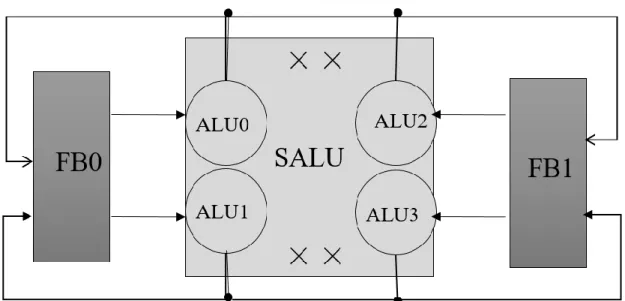
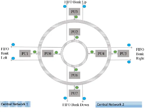
The proposed computing fabric architecture by [3] is comprised of three individual configurable modules i.e. Shared-ALUs, token state machine, and FIFO Banks. The proposed fabric architecture 5×5 is shown in Figure 2-5. As can be seen in this figure, the architecture can be extended in both dimensions. All the computing and routing capabilities of the fabric are concentrated in the SALU, which is consisted of eight independent ALUs, their associated decoder and one central router network, as illustrated in Figure 2-6.
Figure 2-5- CGRA Proposed by Allared [3] © 2010 IEEE
Figure 2-6-The architecture of the SALU [3] © 2010 IEEE
The decoder is used to make the connection between FBs and ALUs. Decoder sends the data token to ALUs to execute the operation. Also, each decoder has two internal buffers to store the operands, temporarily. In order to perform an operation, one operand could come from the adjacent bank, and another one could come from an internal buffer. After executing the operands, the ALU sends the result to the decoder. Thus, the decoder will subsequently forward the result to its final destination
through the network. All routing decisions are performed through the router network. In fact, the network router is the vital element of SALU that allows carrying out all data tokens to their destination according to their respective order.
The network can accept eight tokens per cycle and return the same number to different destinations. The network router consists of six distinct routers with two different types called type1 and type2. Figure 2-7 shows the block diagram of router type1 and type2. The left side of router type1 connects to the ALUs and router type2. The output of router type1 connects to the ALUs, FIFO Banks, and router type2. While the router type 2 only has communication with router type1.
Figure 2-7- Schematic of: a) router type1:router1_0 , b) router type 2: router 2_0 [3] © 2010 IEEE
Each type1router is associated with one side of SALU. In addition, the type 1 router has no contact with other type1, yet they can access to router type 2 to send data token to different paths. A simple round-robin algorithm is used for the network router to send all data token to their destination. The
block diagram of router network is shown in Figure 2-8. In this architecture, routing is performed through the central router network. The network can accept eight tokens per cycle and return the same number of tokens to their destinations.
Figure 2-8-Central Router Network [3] © 2010 IEEE
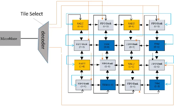
A token state machine is a program unit that stores the required instruction tokens according to a specific application. Instruction can be used in order to control the transmission data tokens between the SALU and RFs. TSM represents the direct interface between the user and the fabric. The instructions must contain all the necessary information to choose the operands, operations, destination, and SALU. Each TSM has eight independent parallel small state machines that each pair corresponds to one FIFO bank.
Figure 2-9 shows the block diagram of a TSM. A FIFO Bank represents the system’s memory, which is connected to the two different modules of SALU and TSM. The synchronization by data is the foundation of the architecture, which happens by using data token. FB manages all the traffic required to route the data token and instructions to SALU. Furthermore, it is possible to make concurrent write and read of data tokens. Each FB consists of 16 independent register files R0 to
The TSM determines the data path and register file. The data token and instruction should be transferred to specified SALU through FBs.
Figure 2-9-Block Diagram of a TSM [3] © 2010 IEEE
2.4 Programming of most popular CGRAs
This section gives the information about the programming of some CGRAs.
2.4.1 Programming REMARK coprocessor
REMARK coprocessor is tightly coupled to a host processor. The programming environment allows programming of both host and coprocessor concurrently. REMARK programming environment is comprised of the REMARK global instruction assembler and the Nano instruction assembler. The GCC compiler programs the host processor. The global instruction assembler begins with global assembly code and generates configuration data and label information. The Nano instruction begins with Nano assembly code and generates the configuration code. Due to utilizing the configurable REMARK architecture, the programmer attaches REMARK assembler instruction into the C program. Using REMARK assembler instruction, the assembled code for the host processor and binary code for REMARK instruction are generated. Finally, the GCC compiler is used again to generate executable code which includes the host processor and the global and Nano configuration data[18][21].
2.4.2 Programming MorphoSys coprocessor
MorphoSys uses GUI-based design tools to compile the application for reconfigurable array and host processor. The programmer has manually to separate the input code between the host processor and reconfigurable array. GUI-based includes mView, mLoad, and MCC. The mView has been developed to help the designer in mapping application to the reconfigurable cells. The mView can operate in two modes, programming mode or simulation mode. Based on both modes, one context file is generated by mView that represents the user-specific application for each cell. For system simulation, each application should be coded into the context words. This context word generates by mLoad using the input file from mView. The MCC is a prototype C language compiler that has been developed to compile code for MorphoSys. After partitioning the code between the host processor (TinyRISC) and the RC arrays, the MCC generates the instructions for TinyRISC processor. These instructions can control the RC array execution for parallel computation[18][27][25].
2.4.3 Programming PipeRench Architecture
The PipeRench compiler maps computations described in a dedicated intermediate single-assignment language so-called DIL into the PipeRench. As mentioned earlier, the PipeRench made up of columns of pipeline stages and the model of the configuration of computation stage which can use the execution of the next stage in the current stage. DIL can be observed as a language to exhibit an intermediate representation of high-level language description such as C. It can also be used to describe pipelined combinatorial circuits. The compiler employs the same internal representation to perform synthesis, optimization and place and route. The compiler constructs a hierarchical acyclic data flow graph as an intermediate representation of the application. The DFG has nodes and edges where nodes represent the operations and edges represent the operands. After the generation of global application’s DFG, the compiler does some optimizations over DFG; such optimization includes traditional compiler optimization, for example, common subexpression elimination, algebraic simplification, and dead code elimination. The placement and routing phase is performed via DFG by a deterministic linear-time algorithm which is based on list scheduling[24].
2.4.4 Programming RaPiD Architecture
The programming of RaPiD performs using RaPiD-C, a C-like a language to help the programmer to a map of high-level computation description to the RaPiD architecture. RaPiD-C allows the programmer to specify the parallelism, data movement, and partitioning. The mechanism Wait and Signal are used by RaPiD-C for synchronization and assign right data into the RAM [30], [31].
2.4.5 Different techniques of the mapping applications on the CGRAs
This section provides a brief study of the state-of-the-art methods in mapping applications on the CGRAs.
Ricardo et al. presented a Just-In-Time module scheduling for the mapping application onto CGRA. Their proposed algorithm combines three distinct methods such as a mapping algorithm, a crossbar network, and virtual coarse-grained reconfigurable architecture. A module scheduling algorithm is used in the mapping algorithm to map loops into virtual CGRA. The algorithm is based on a greedy heuristic, and virtual CGRA is a layer on top of FPGA. They have also proposed a CGRA based on crossbar network instead of mesh topology network [32].
The resource constrained mapping of DFG onto CGRA has been presented by Naifeng. The resource constrained mapping problem is formulated using ILP; the produce optimal result is created by ILP for the mapping of the DFG onto the CGRA. In order to accelerate the problem-solving, they have also proposed a heuristic algorithm by using the maximum flow minimum cut algorithm for practical use and large problem[33].
In data-driven mapping using local patterns presented by Gayatri, to accelerate the mapping application on to CGRA, a database of an example of high-quality mapping has been used based on a search tree. The depth of search tree is reduced using placing pattern of nodes instead of single ones. The anytime A* algorithm proposed in this research to find a good solution and improve that solution to place a node on the CGRA. Anytime A* is a greedy algorithm that provides a solution within certain bound to solve the problem of mapping of DFG on to CGRA. To solve the problem mentioned above, they have also used the Anytime Multiline Tree Rollup method in which they try to keep all solution paths diverse to ensure that results from previous steps are stored to avoid
repetition and traversing path. They have claimed that their proposed method outperforms the simulated annealing algorithm to placement and routing nodes onto CGRA[34].
Akira et.al have proposed modulo scheduling algorithm to compile loops in a program onto CGRA. Their algorithm consists of resource reservation phase and scheduling algorithm. The resource reservation phase guarantees the resources needed at the steady state such as FUs consumed by operation and routing resources. Resource-aware placement algorithms were proposed to shorten the solution time. In order to map an application onto target architecture, a compact graph has been used in [35].
Yuanqing has proposed an algorithm to map applications written in a high-level language program such C onto CGRA. His proposed algorithm contains 4 phases such as translating source code to a control data flow graph, task clustering and ALU data path mapping, scheduling and resource allocation. In the first phase, the input C program translated into CDFG and some optimization and simplification perform on the CDFG. In the second phase, the CDFG is partitioned into several tasks to assign them on to ALU. In the third phase, the clustered graph is scheduled and mapped to an unbounded number of fully connected ALUs. Finally, the last phase, the scheduled graph in prior phase is assigned to ALU and in the phase, the other resources such as buses, register, memories, etc. are assigned[36].
A routing-aware mapping algorithm has been presented for CGRA by Ganghee. An integer linear programming has been considered for Steiner point routing, i.e., for optimal map application onto CGRA instead of spanning tree based routing. In addition, a fast heuristic mapping algorithm for CGRA that is based on routing aware and incorporated of Steiner point has been presented. The heuristic algorithm contains two phases: list scheduling and quantum-inspired evolutionary algorithm. Using list scheduling the constructed CDFG from the application is scheduled with the given resource constraint to get the initial solution and determine the priority of the node. Dijkstra algorithm is used to find the shortest path between two PEs. The QEA is like a genetic algorithm, and it evaluates each case to reach the best answer of mapping CDFG on to CGRA[37], [38]. Mapping application onto reconfigurable KressArrays proposed by Hartenstein. KressArrays consists of a mesh of a PEs which is also known as reconfigurable data path units. The application
written in a high-level programming language are placed and routed on the rDPUs using simulated annealing. A given data path would place and routed on the hardware using simulated annealing based mapper [23][39].
Hyunchul proposed a software pipelining technique for CGRA that leverages module graph embedding referred to graph embedding from graph theory. To place the operations of loop body of the application on CGRA, they have presented three dimensions of CGRA that two of them are related to the FUs and third dimensions assigned to time slots. Module scheduling performed with each set of the operations which are located in the same level of DFG. Three-dimensional scheduling grid is filled for each group of scheduled operation by the skew manner in considering with restricted FUs and time slot available. Also, some cost functions are defined between pair DFG of nodes to reduce the routing path and optimize place and route. These functions are routing cost, affinity cost, and position cost. Routing cost guarantees that producers and consumers are placed close to each other. Affinity cost ensures that the producers with common consumers in DFG are placed together. Finally, position cost ensures that the operations are left-justified on the set of appropriate resources[40].
EMS for CGRA is a research issue in continues of previous work of Hyunchul. Modulo scheduling is a technique in software pipeline of loops to exploit the parallelism of the CGRA. EMS tries to perform the routing of the nodes instead of place nodes first and routing paths followed by placement. During the routing process, if there is a path from the source to the destination of DFG of nodes then placement is done after the routing[41].
Chen has proposed minor graph approach for mapping application onto CGRA. The CGRA mapping problem has been formalized as a graph minor of the module routing resource graph representing the CGRA resources and their interconnects [42].
A retargetable compiler, known as Dynamically Reconfigurable Embedded System Compiler proposed by Mei. He proposed a module scheduling algorithm based on simulated annealing to placement and routing operands on the CGRA. This compiler can parse, analyze transform and schedule plain C program to CGRA[43][44].
Mei introduces a modulo scheduling algorithm to exploit loop level parallelism on CGRA in 2003. Modulo scheduling algorithm used in integer linear program processor such as VLIW to improve the parallelism by executing different loop iteration in parallel. Also modulo routing resource graph proposed as an abstraction of hardware description and enforce to modulo constraint. The proposed algorithm combines the FPGA place and route algorithm with modulo scheduling to achieve a mapping of application onto CGRA [45].
2.4.6 Modulo Scheduling
Modulo Scheduling is a software pipelining technique employed to utilize instruction-level- parallelism in the loops body using overlapping consecutive iterations. The loop body is represented as a data flow graph where the nodes represent the operations, and the edges represent the data dependency among the operations. MS tries to find a pattern to develop it by several iterations of operations. MS utilizes a different approach in which the operation’s placement is performed in a cyclic interpretation without any resource conflicts and data dependency violations. The scheduling process includes three stages such as Prolog, Kernel, and the Epilog. The kernel corresponds to the steady-state execution in different consecutive iterations. The instructions of a repetitive pattern of operations are called kernels[46][47].
The goal of MS is to find a valid schedule in which the Initiation Interval (II) is minimized. II is the delay between two successive iterations of the loop body. Ideally, all the loop bodies are processed in parallel (II=0) if there are no dependencies and enough hardware resources. In the worst case scenario, the next iteration of the loop body cannot start before the current one is finished. Initially, the scheduler begins with Minimum II (MII) value between the maximum values of the recurrence-constraints lower bound (RecMII) and the resource constraints lower bound (ResMII). However, if a valid MS cannot be found, the scheduler increases the II by one, and the scheduling is attempted again to find a possible valid MS [42].
MS attempts to explore one model of nodes in DFG that can be executed at the same level. This model, as discussed earlier, is called kernel. The kernel consists of a pattern of DFG nodes. The nodes can be executed as pipeline thanks to the specified pattern. To compute-intensive kernels with high efficiency and flexibility, CGRA architectures are the best candidates. Accordingly, the
modified MS is a popular method to map an application in the form of DFG to the CGRA [42], [46][47].
2.4.7 Modulo Scheduling and CGRA
Modulo scheduling is widely used software pipelining technique that is capable of compiling DFG onto a family of heterogeneous CGRA. The goal of mapping is to generate a schedule that explicitly combined with place and route the operation that the application throughput is maximized. This criteria throughput is indicated using initiation interval by modulo scheduling. The II is essentially reflecting the performance of the scheduled and P&R applications onto CGRA, and it plays a central role in exploiting parallelism. Various algorithms have been developed for VLIW processors. However, they have not been successfully applied for CGRA architecture. In another word, the CGRA complexity architecture is much higher than VLIW, due to the complex architecture of CGRA. Thus, the key metric used to map an application onto CGRA is II [32][41]– [43].
The mapping application using MS onto CGRA may give rise to add some different approaches to the scheduler. This difference for scheduling application is mostly due to the hardware characteristics of the CGRA. Modulo scheduling for CGRA considers the scheduling, placement and routing the operations onto function units. Placement determines on which FU of a 2-Dimensional array will place an operation. Scheduling determines in which cycle, an operation can be executed. Finally, routings will connect the placed and scheduled operations according to their data dependencies [32][41]–[43].
In order to map the kernel (defined in Module Scheduling) onto CGRA, each particular cycle of the kernel is mapped on each II configurations of CGRA, where each configuration is referred to one configure the mapping of nodes onto CGRA. Configurations can be stored as a Configuration Context (CC) for CGRA, and they can be updated in every cycle. The CC specifies the functionalities and connectivity among FUs. The CC also includes the direction for each FU to determine where to get its input from prior cycle and where to write its output for the next cycle. In fact, CC is a valid mapped configuration of DFG nodes onto CGRA.
2.4.8 Summary of CGRA mapping algorithms
The characteristics of particular CGRA mainly effect on the compilation techniques. Most CGRAs architectures are non-FPGA based that is coupled to a general purpose processor as a co-processor. Given this, compiling such systems are not as a generic problem similar FPGA-based, because the FPGAs-based has a standard architecture [48] [49].
An overview of placement and routing by well-known CGRA architectures is given in Table 2-1. It can be seen from this table the structure of the CGRA architecture has an important impact on the placement phase. Heuristic placement based on SA and genetic algorithms has been borrowed in synthesis systems for FPGAs [20][18]. PADDI is used a scheduling algorithm in order to resource allocation [20][18][50]. The routing based on greedy algorithms is used only in cases where the routing is restricted to one dimension. Also, the P&R result based on greedy algorithms would not be satisfied as well. The domain specifies which kind of applications can be executed on CGRA, as mentioned in Table 2-1.Table 2-2 provides the summary of the recent mapping algorithms on the CGRAs.
Table 2-1- properties of programming environment of CGRA.
CGRA Programming Placement Routing Coupling Domain
REMARC[26] Assembly Manual Manual Coprocessor MM
RaPiD[22] RaPiD-C SA Pathfinder Loose DSP
PipeRench[24] DIL Greedy Linear Greedy Coprocessor Data-Stream
Pleiades [50][20] C/C++ Direct - Coprocessor DSP
MorphoSys[25] C Manual Manual Tight DSP&MM
KressArray[39] ALE-X SA Neighbor Loose General-purpose
GARP[51] C Tree-matching Greedy Coprocessor General-purpose
PADDI[20][50] Silage By Scheduling Direct Loose DSP
MATRIX[52] Assembly Manual Manual Loose General-purpose
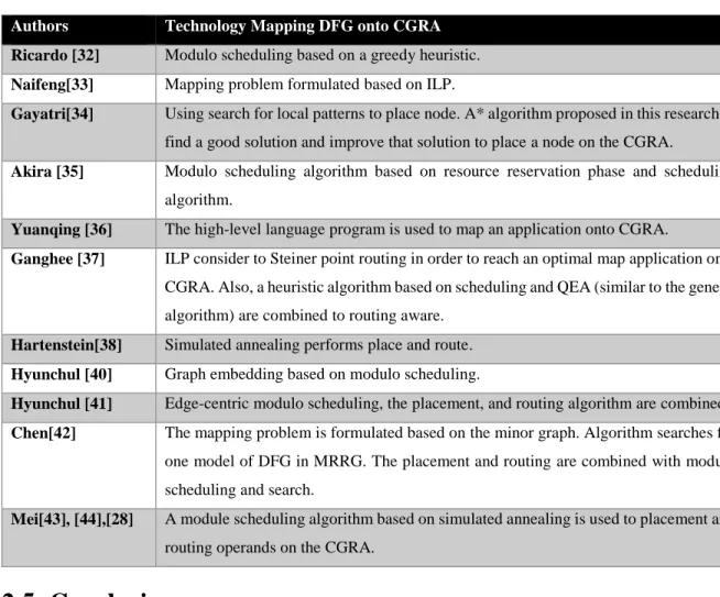
Table 2-2-Technology mappings in recent years. Authors Technology Mapping DFG onto CGRA
Ricardo [32] Modulo scheduling based on a greedy heuristic.
Naifeng[33] Mapping problem formulated based on ILP.
Gayatri[34] Using search for local patterns to place node. A* algorithm proposed in this research to find a good solution and improve that solution to place a node on the CGRA.
Akira [35] Modulo scheduling algorithm based on resource reservation phase and scheduling algorithm.
Yuanqing [36] The high-level language program is used to map an application onto CGRA.
Ganghee [37] ILP consider to Steiner point routing in order to reach an optimal map application onto CGRA. Also, a heuristic algorithm based on scheduling and QEA (similar to the genetic algorithm) are combined to routing aware.
Hartenstein[38] Simulated annealing performs place and route.
Hyunchul [40] Graph embedding based on modulo scheduling.
Hyunchul [41] Edge-centric modulo scheduling, the placement, and routing algorithm are combined.
Chen[42] The mapping problem is formulated based on the minor graph. Algorithm searches for one model of DFG in MRRG. The placement and routing are combined with modulo scheduling and search.
Mei[43], [44],[28] A module scheduling algorithm based on simulated annealing is used to placement and routing operands on the CGRA.
2.5 Conclusion
In this chapter, a review of the literature on topics specific to CGRAs along with mapping applications algorithms has been presented.
Several researchers have proposed some algorithms to compile a program to automatically map an application onto CGRA. There are numbers of automatic design and compiling tools developed to exploit the massive parallelism found in applications and extensive computation resources of CGRA. Some researchers utilize structure or GUI-based design tools to manually generate a design that would be difficult to handle big designs. Some other have only focused on Instruction-Level Parallelism that failed to make utilization of the CGRA efficiently and in principle cannot result in higher parallelism than VLIW. However, ILP is limited in scope and fail to make resources
![Figure 2-3-REMARK Architecture [26] © 1998 IEEE.](https://thumb-eu.123doks.com/thumbv2/123doknet/2334288.32433/31.918.264.656.126.453/figure-remark-architecture-ieee.webp)
![Figure 2-4-EGRA Architecture[29] ©2010 IEEE](https://thumb-eu.123doks.com/thumbv2/123doknet/2334288.32433/32.918.303.635.207.501/figure-egra-architecture-ieee.webp)
![Figure 2-7- Schematic of: a) router type1:router1_0 , b) router type 2: router 2_0 [3] © 2010 IEEE](https://thumb-eu.123doks.com/thumbv2/123doknet/2334288.32433/34.918.117.778.409.864/figure-schematic-router-type-router-router-router-ieee.webp)