To cite this document:
Martin-Gonthier, Philippe and Molina, Romain and
Cervantes, Paola and Magnan, Pierre Analysis and Optimization of Noise
Response for Low-Noise CMOS Image Sensors. (2012) In: 10th IEEE NEWCAS
2012, 17-20 Jun 2012, Montreal, Canada.
OATAO is an open access repository that collects the work of Toulouse researchers and
makes it freely available over the web where possible.
This is an author-deposited version published in:
http://oatao.univ-toulouse.fr/
Eprints ID: 6669
Any correspondence concerning this service should be sent to the repository
administrator:
[email protected]
Abstract— CMOS image sensors are nowadays widely used in
imaging applications and particularly in low light flux applications. This is really possible thanks to a reduction of noise obtained, among others, by the use of pinned photodiode associated with a Correlated Double Sampling readout. It reveals new noise sources which become the major contributors. This paper presents noise measurements on low-noise CMOS image sensor. Image sensor noise is analyzed and optimization is done in order to reach an input referred noise of 1 electron rms by column gain amplifier insertion and dark current noise optimization. Pixel array noise histograms are analyzed to determine noise impact of dark current and column gain amplifier insertion. Transfer noise impact, due to the use of pinned photodiode (4T photodiode), is also measured and analyzed by a specific readout sequence.
Index Terms—CMOS Image sensors, dark current noise,
pinned photodiode, low-light flux, Column gain amplifier
I. INTRODUCTION
CMOS image sensors are nowadays extensively used in commercial, scientific and space applications [1]-[3]. CMOS standard processes, which are developed for digital and mixed signal applications, are really attractive particularly because of their low power consumption, applicability for on-chip signal processing and large availability. Several ways have been explored to improve image sensor performances to a very high level and performances have been significantly enhanced with the use of CIS (CMOS Image Sensor) processes [4], [5]. Image sensors performances are described by key parameters which are Quantum Efficiency (QE), Conversion gain (CG), Dark Current (DC), Noise, Full Well Capacity (FWC), Photo-Response and Dark Signal Non-Uniformities (respectively PRNU and DSNU) and Modulation Transfer Function (MTF). Low light applications require low noise image sensors leading to noise optimisation of image sensors [6]. This noise reduction is really possible thanks to the use of pinned photodiode associated with a Correlated Double Sampling (CDS) readout. It reveals new noise sources which become the major contributors. This paper presents optimisations done to reach an input referred noise of 1 electron rms.
First part of section II describes a common readout circuit of a pinned photodiode imager. Then, noise model is depicted in relation with this common readout circuit. The last part of section II analyzes the noise contributor impacts and optimization means. Test vehicle with optimizations and associated noise measurement results are described in section
III. In addition, a specific readout sequence is applied in order to show transfer noise impact due to the use of pinned photodiode on total noise. Section IV presents the conclusions and perspectives of this work.
II. NOISE MODEL OF CMOSIMAGE SENSOR
A. Common CMOS image sensor readout circuit
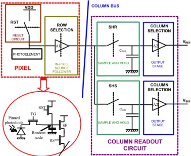
A common CMOS image sensor readout circuit architecture is shown in Fig. 1. It is composed of a photo-element: a pinned photodiode associated with a transfer gate; a reset switch allowing to reset the readout node; an in-pixel source follower which drives the signal from pixel to column readout circuit; a double sample and hold circuit for reference and integrated signal levels; an output stage allowing to drive the signal off chip or on chip for additional processing.
IN-PIXEL SOURCE FOLLOWER PHOTOELEMENT PIXEL COLUMN BUS Pinned photodiode TG RST RS SF Readout node VREF COLUMN READOUT CIRCUIT RST ROW
SELECTION SHR SELECTION COLUMN VDD
RESET CIRCUIT
SAMPLE AND HOLD OUTPUT STAGE A1 A2 CSHR VSIG SHS COLUMN SELECTION OUTPUT STAGE A2 CSHS
SAMPLE AND HOLD
Fig. 1. Common readout circuit architecture of a CMOS image sensor
For a pinned photodiode pixel (4T), before the end of the integration time, the readout node is reset by the reset MOSFET (command signal RST). This level, called reference, is sampled and held (command signal SHR) in the column readout circuit in the reference channel via the in-pixel source follower (SF) and the row selection (RS) transistor. Then, the charge transfer from the photodiode to the readout node begins (signal TG). When the charge transfer is done, a voltage level corresponding to the integrated charges is sampled and held (command signal SHS) in the column readout circuit of the signal channel. Video signal voltage level results from the
Analysis and Optimization of Noise Response for Low-Noise
CMOS Image Sensors
P. Martin-Gonthier, R. Molina, P. Cervantes, P. Magnan
ISAE, Université de Toulouse, 10 avenue E. Belin, 31055, Toulouse, France
[email protected]
subtraction of the two samples (reference and signal). This readout sequence allows reset noise cancellation by CDS sequence.
B. Common CMOS image sensor readout circuit noise model
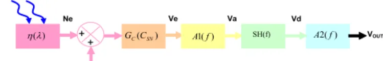
The previous common CMOS image sensor readout circuit can be modeled by the synoptic diagram shown in Fig. 2, where e is the photon flux, NDC is the number of electrons
corresponding to dark current integrated during photodiode integration time, η(λ) is the quantum efficiency, GC is the
conversion gain (depending on the sense node capacitance CSN), A1(f) is the first stage gain, SH(f) is the transfer function
of the sample and hold circuit and A2(f) is the output stage gain. PHOTON FLUX ) ( GC(CSN) A1 f( ) SH(f) A2 f( ) e Ne Ve Va Vd VOUT NDC + +
Fig. 2 : Common CMOS image sensor readout circuit synoptic diagram
This synoptic diagram leads to the following transfer function: ) ( ) ( ) ( ) ( ) ) ( ( N G C A1 f SH f A2 f VOUT e DC C SN where
VOUT is the output signal.
Fig. 3 shows the complete synoptic diagram including noise sources. PHOTON is the photon noise in electrons, DC is the
noise induced by dark current in electrons,RECHARGE is the
reset noise [7] in volt, A1+SH is the first stage and sample and
hold noise in volt andA2 is the output stage noise in volt.
PHOTON FLUX PHOTON NOISE PHOTON RESET NOISE (SENSE NODE) RESET
NOISE FROM SOURCE FOLLOWER ASSOCIATED TO SAMPLE AND HOLD CIRCUIT
SH A 1
OUTPUT CIRCUIT (SOURCE
FOLLOWER) NOISE 2 A DARK CURRENT NOISE DC ) ( GC(CSN) ) ( & ) ( 1 f SH f A A2 f( ) e s Ne Ns Ve Vi Va Ve VOUT NDC DARK CURRENT
Fig. 3: Common CMOS image sensor readout circuit noise model
Noise sources are uncorrelated leading to the following CMOS image sensor noise equation (1):
2 2 2 / 1 2 2 2 2 2 2 1 2 2 2 2 1 2 2 2 2 2 1 2 2. . . . . . . . . 2. . 2. ) ( C PHOTON C DC RESET A SH A TOTV G A A G A A A A A (1) Due to the differential readout sequence in order to obtain video signal (subtraction between reference and signal samples), noise power spectral densities from first stage source follower associated with sample and hold circuit and output stage source follower are doubled and reset noise is canceled leading to the simplified noise equation in darkness in volt rms (2): 2 2 2 / 1 2 2 2 2 2 2 1 2. . . 2. . 2. ) ( C DC A S H A TOT V G A A A (2)
Finally, the input referred noise in electrons can be expressed by the following equation (3) when the sensor is in the darkness: 2 2 2 1 2 2 2 2 1 2 2 / 1 2 . . . 2 . . 2 ) ( A A G A G e C A C H S A DC TOT (3)
C. Noise response optimization
As can be seen in the previous equation, different ways exist to minimize the noise response:
Minimize in-pixel amplifier stage (source follower) and output stage (source follower). This minimization can be done by design optimizations (such as biases current, W and L MOSFET size or bandwidth settling).
Increase conversion gain GC by reducing sense (or
readout) node capacitance. The conversion gain, which is the diffusion of the sense node, depends on the technology used. Sense node capacitance design with minimum layout rules leads to maximum conversion gain value.
Minimize dark current value. Indeed, noise coming from dark current follows the Poisson law. The dark current value also depends on the technology used.
Increase the gain of the readout chain. Indeed, if A1 or A2
increase, input referred noise will be lower. However, due to topological constraints, an enhanced amplifier cannot be implemented in-pixel. Only insertion of gain in the column can be implemented.
This paper is focussed on the noise optimization by reducing dark current noise and by increasing readout circuit gain with a column gain amplifier insertion. Therefore, the two last optimizations are presented in the next paragraph.
1) Dark current optimization
Dark current sources are shown on Fig. 4 [8]. There are mainly two sources of dark current in a photodiode: Firstly, current due to defect sites (a); and secondly current due to injection or off-leak (b). Only optimization on the defect sites is done in this paper.
Fig. 4 : Dark current sources at the pixel level
Two locations of defect sites can be observed: defects between STI and photodiode and defects coming from SiSiO2 interfaces
near the transfer gate transistor. CIS process offers optimised photodiode where defects between STI and photodiode are well passivated. Previous works show good results on dark current minimization due to the traps near the transfer gate transistor [8], [9]. By applying a negative bias during the integrating phase on the transfer gate, a significant dark current
reduction is observed. Indeed, during the transfer gate negative bias, the transistor is in accumulation and thermally generated electrons can recombine with accumulated holes.
2) Column gain amplifier insertion
The other way to reduce noise is to minimize the input referred noise by increasing the readout chain gain as can be seen in Fig. 5 and in [10], [11]. However, due to pixel topological constraints, no complex amplifier can be done in-pixel. Thus, the gain amplifier is inserted in the column where topological constraints are lower.
IN-PIXEL SOURCE FOLLOWER PHOTOELEMENT PIXEL COLUMN BUS ROW SELECTION AG PHI1 C2 C1 PHI2 PHI3 COLUMN GAIN AMPLIFIER VREF
SAMPLE AND HOLD CIRCUIT AND OUTPUT STAGE RST
ROW
SELECTION SHR SELECTION COLUMN
VDD
RESET CIRCUIT
SAMPLE AND HOLD OUTPUT STAGE A1 A2 CSHR VSIG SHS COLUMN SELECTION OUTPUT STAGE A2 CSHS
SAMPLE AND HOLD
Fig. 5 : Readout chain with column gain amplifier inserted
From Fig. 5, the input referred noise in electron becomes (4): 2 2 2 1 2 2 2 2 2 1 2 2 / 2 2 1 2 2 1 2 . . . 2 . . . 2 . ' . 2 ) ( A A G A A G A G e C A G C H S AG C A DC TOT (4)
where ’A1 is the noise corresponding to the in-pixel amplifier
with new bandwidth due to column gain amplifier insertion, AG is the noise from the column gain amplifier inserted and
S/H is the noise coming from sample and hold circuits. This
equation shows the input referred noise coming from the output stage and sample and hold circuit is reduced. In addition, noise from the in-pixel amplifier can be minimized by adjusting in-pixel amplifier biases and bandwidth.
III. TEST VEHICLE DESCRIPTION AND MEASUREMENTS
A test vehicle was designed in a CIS 0.18µm technology. It is a 256x256 pixel array with pinned photodiode (4T) and 7µm pixel pitch. The pixel array is composed of 5 sub-arrays:
One sub-array with common readout circuit (without column gain amplifier inserted).
Four sub-arrays named G1, G10, G20 and G30 with column amplifier inserted respectively with the following gain values: 1, 10, 20 and 30.
Fig. 6 shows a microphotography of the test image sensor designed.
Fig. 6 : Photography of the test image sensor
Noise measurements were done in order to evaluate impacts of dark current minimization and column gain amplifier insertion on the noise test image sensor. At first, dark current measurements were done to check its reduction when the transfer gate transistor was biased with negative voltage during integration time on the first sub-array of pixel with the common readout chain. Measurement results show a dark signal of 67electrons/s/pixel when no negative bias is applied to the transfer gate. This dark signal decreases drastically (64%) when a negative bias of -0.5V is applied. A value of 24electrons/s/pixel is measured. The dark signal reduction impact is depicted in Fig. 7 with the noise histogram of the sub-array with common readout circuit. Due to a tail in the various histograms, mean and median values are extracted. A slight noise reduction is observed between the two biases of the gate transfer. However, the other noise sources seem to be dominant.
Fig. 7 : Input referred noise histogram (all the pixels of the sub-array) for common readout circuit with and without negative transfer gate bias during
integration time
Fig. 8 shows the noise histogram of sub-array G30 corresponding to a column amplifier inserted in the readout chain (gain of 30) with and without a negative bias applied to the transfer gate. A higher noise reduction is reached.
Fig. 8 : Input referred noise histogram for readout circuit with column amplifier inserted (gain of 30) with and without negative transfer gate bias
during integration time
Table 1 shows the noise measurement results in electrons (rms) for the different readout chain types (common, G1, G10, G20 and G30) corresponding to the 5 pixel sub-arrays with negative bias applied to the transfer gate (-0.5V) during integration. These results show significant noise reduction when the gain of the inserted column amplifier is high.
However, when gain of the column amplifier is 1, an increase of the noise is observed. This is due to the insertion of the new noise source (corresponding to the inserted column amplifier) which is not reduced by the gain.
Table 1 : Noise measurements with the different readout chain (common, G1, G10, G20 and G30) with a negative bias of -0.5V for transfer gate during
integration
As can be seen, a very low noise is reached for higher gains.
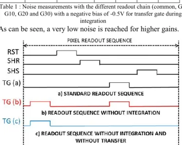
Fig. 9: Specific readout sequence: a) standard readout sequence; b) readout sequence to eliminate dark signal impact; c) readout sequence to eliminate
dark signal impact and transfer noise
In order to determine where improvements can be made on the readout chain where column amplifier is inserted, other measurements were done. Specific chronograms, shown in Fig. 9, were applied. Fig. 9a shows the standard readout sequence of a pixel. Fig. 9b depicts the readout sequence with no integration. Indeed, a transfer is done before the sampling of the reset of the readout node leading to no integrated charge transferred. Fig. 9c illustrates the readout sequence with no integration and no transfer done between the reference (SHR) and signal SHS) samples.
Fig. 10 : Input referred noise histogram for readout circuit with column amplifier inserted (gain of 30) with and without negative transfer gate bias
during integration time
Noise measurements from the sub-array G30 (column amplifier inserted in readout chain with a gain of 30) with negative bias applied to the transfer gate (-0.5V) during integration are illustrated in Fig. 10 and show the impact of the dark signal remaining and the transfer noise. The remaining dark signal has no impact on the noise. The transfer noise has only a slight impact on the total noise. This means the dominant noise sources are in the readout chain despite insertion of column amplifier with high gain. So, in order to reduce the total noise value, an enhanced optimization has to be made to reach sub-electron input referred noise.
IV. CONCLUSIONS
This work shows the noise impact of optimization of dark signal and column amplifier insertion in the common CMOS image sensor readout chain. Noise mean values of 1.51 electron rms are measured with a column amplifier gain of 30 and negative bias applied to the transfer gate (-0.5V) during integration. Specific readout sequences are applied to determine the impact of transfer noise and remaining dark signal on the total image sensor noise. Noise measurements show a slight impact of these parameters once optimization is done.
REFERENCES
[1] E.R. Fossum, “CMOS image sensors: electronic camera-on-a-chip”, Electron Devices, IEEE Transactions on, vol.44, no.10, pp.1689-1698, October 1997.
[2] T. Lule, S. Benthien, H. Keller, F. Mutze, P. Rieve, K. Seibel, M. Sommer, M. Bohm, “Sensitivity of CMOS based imagers and scaling perspectives”, Electron Devices, IEEE Transactions on, vol.47, no.11, pp.2110-2122, November 2000.
[3] P. Martin-Gonthier, P. Magnan, F. Corbiere, S. Rolando, O. Saint-Pe, M.B. de Boisanger, F. Larnaudie, “CMOS detectors for space applications: from R&D to operational program with large volume foundry”, Sensors, Systems, and Next-Generation Satellites XIV, SPIE, 2010, 7826.
[4] M. Furumiya, H. Ohkubo, Y. Muramatsu, S. Kurosawa, F. Okamoto, Y. Fujimoto and Y. Nakashiba , “High sensitivity and No-Crosstalk pixel technology for embedded CMOS Image Sensor”, Electron Devices, IEEE Transactions on, Vol. 48, NO. 10, October 2001.
[5] O.-B. Kwon and al, « An improved digital CMOS imager », in Proc. IEEE Workshop Charge-Coupled Devices and Advanced Image Sensors, June 1999, pp. 144-147.
[6] B. Fowler, C. Liu, S. Mims, J. Balicki, W. Li, H. Do, P. Vu, “Low-light-level CMOS image sensor for digitally fused night vision systems”, rn F. Andresen, B.; Fulop, G. F. & Norton, P. R. (ed.), Infrared Technology and Applications XXXV, SPIE, 2009, 7298, 72981D.
[7] B. Fowler and al, «Reset noise reduction in capacitive sensors», IEEE Transactions on Circuits and Systems, Vol.53, N°8, Aug. 2006. [8] T. Watanabe, J-H Park, S. Aoyama, K. Isobe and S. Kawahito, “Effects
of Negative-Bias Operation and Optical Stress on Dark Current in CMOS Image Sensors”, Electron Devices, IEEE Transactions on, 2010, 57, 1512 -1518
[9] B. Mheen, Y-J Song and A. Theuwissen, “Negative Offset Operation of Four-Transistor CMOS Image Pixels for Increased Well Capacity and Suppressed Dark Current”, Electron Device Letters, IEEE, 2008, 29, 347 -349
[10] N. Kawai and S. Kawahito, “Noise analysis of high-gain, low-noise column readout circuits for CMOS image sensors”, Electron Devices, IEEE Transactions on, 2004, 51, 185 - 194
[11] M. Sakakibara, S. Kawahito, D. Handoko, N. Nakamura, H. Satoh, M. Higashi, K. Mabuchi and H. Sumi, “A high-sensitivity CMOS image sensor with gain-adaptive column amplifiers”, Solid-State Circuits, IEEE Journal of, 2005, 40, 1147 - 1156
READOUT CHAIN TYPE
(negative bias of -0.5V applied to the transfer gate during integration) COMMON G1 G10 G20 G30 INP UT RE F E RR E D NOIS E (e - rm s) MEAN VALUE 3.27 5.62 1.68 1.64 1.51 MEDIAN VALUE 2.66 5.07 1.25 1.20 1.10