HAL Id: hal-02656773
https://hal-amu.archives-ouvertes.fr/hal-02656773
Submitted on 5 Jun 2020
HAL is a multi-disciplinary open access
archive for the deposit and dissemination of
sci-entific research documents, whether they are
pub-lished or not. The documents may come from
teaching and research institutions in France or
abroad, or from public or private research centers.
L’archive ouverte pluridisciplinaire HAL, est
destinée au dépôt et à la diffusion de documents
scientifiques de niveau recherche, publiés ou non,
émanant des établissements d’enseignement et de
recherche français ou étrangers, des laboratoires
publics ou privés.
Tunable electrical properties of self-organized zirconia
nanotubes
Florence Vacandio, Marielle Eyraud, Philippe Knauth, Thierry Djenizian
To cite this version:
Florence Vacandio, Marielle Eyraud, Philippe Knauth, Thierry Djenizian. Tunable electrical
proper-ties of self-organized zirconia nanotubes. Electrochemistry Communications, Elsevier, 2011, 13 (10),
pp.1060-1062. �10.1016/j.elecom.2011.06.032�. �hal-02656773�
Tunable electrical properties of self-organized zirconia nanotubes
Florence Vacandio
⁎
, Marielle Eyraud, Philippe Knauth, Thierry Djenizian
LCP, Electrochemistry of Materials Research Group, UMR 6264, Aix-Marseille University, CNRS, Campus de Saint-Jérôme, Marseille cedex 20, F-13 397, France
a b s t r a c t
a r t i c l e i n f o
Keywords: Zirconia nanotubes Nanostructuration Anodization Electrical propertiesStructural and electrical properties of self-organized zirconia nanotube layers can be tuned by a simple thermal treatment. The effect of F on the electrical conductivity of the MOxnanotubes grown by anodization in
fluoride-containing electrolytes is demonstrated.
1. Introduction
Zirconia is known to have remarkable properties and to be an electrical insulator which can become a pure ionic conductor if doped (Y2O3, Gd2O3…)[1,2]. This leads to technological applications such as
industrial catalysts and catalyst supports[3], oxygen sensors[4], solid electrolyte fuel cells (SOFC)[5]. Pure zirconia can be found in three crystallographic structures: monoclinic until 1170 °C, tetragonal between 1170 °C and 2370 °C and cubic above 2370 °C. However, only the tetragonal phase gives ceramics with satisfying mechanical properties. This phase can be stabilized at room temperature by doping with bivalent or trivalent cations, especially by yttrium. During the last decades, the use of porous materials has attracted attention in various domains and particularly in thefield of energy. Porous materials have the advantage of large specific surface that can increase the performances of the materials while reducing the size and weigth of the components. A possible way to grow highly-ordered nanostructures is the anodization of valve metals such as Ti[6,7], Hf
[8], Zr [9–16] in fluoride-containing electrolytes. Most of these nanostructured oxides are obtained by anodization of metallic foils, which limits their application in functional microdevices. An interesting alternative opening the path towards a wide range of applications is the anodization of thinfilms. Thus, in previous work, we have reported the synthesis of self-organized TiO2nanotubes from
sputtered Ti thin layers deposited on Si[17–24].
In this paper, we report the fabrication of ZrO2nanotubes (ZrO2nt)
by anodization of thin layers of Zr deposited by cathodic sputtering on Si substrates. We study the influence of annealing upon the
morphological, structural and electrical properties of nanotubes by Scanning Electron Microscopy (SEM), Energy Dispersive Spectrocopy (EDS), X-ray Diffraction (XRD) and Electrochemical Impedance Spectrocopy (EIS) measurements.
2. Experimental section
Zirconium thinfilms were deposited by cathodic sputtering using a DC triode system on Si substrates (4 × 4 cm2) prepared from p-type Si (100) wafers with a resistivity of 1–10 Ω.cm (Wafer World, Inc.). In order to remove the native oxide layer, the Si samples were dipped in 1% HF solution for 30 s, then rinsed in deionized (DI) water and dried under a nitrogen stream before being introduced into the chamber. A Zr metal disk (nominal purity 99.9%, diameter 5 cm) was the sputtering target and the base chamber pressure prior to depositions was kept as low as 10− 7mbar. The high-purity argon pressure and the target current during deposition were maintained at constant values of 7.10− 4mbar and 150 mA, respectively. Under these conditions, the deposition rate was 16 nm min− 1and a 2.6μm thick Zrfilm was obtained after 120 min. Zirconium layers were anodized at room temperature at 40 V during 10 min with a conventional two-electrode configuration, using an EG&G PARSTAT 2273 potentiostat/ galvanostat. A platinum grid was used as counter electrode. The electrodes were immersed in a 0.35 M NH4F, 5% vol. water and
glycerol electrolyte.
Impedance measurements were performed in a 1 M (NH4)2SO4
solution with in addition to the previous configuration a reference Calomel Saturated Electrode (ECS), using a Potentiostat–Galvanostat coupled with a Frequency Response Analyser (Solartron 1287 and 1260). Impedance diagrams were recorded at open circuit potential, with a signal amplitude of 20 mV and a frequency range starting from 100 kHz to 10 mHz. Samples were analyzed by X-Ray Diffraction ⁎ Corresponding author. Tel.: +33 491 551837; fax: +33 491 551850.
(XRD) with CuKα radiation (λ=0.15406 nm) using a Siemens D5000 diffractometer; the processing software is BRUKER Diffrac-eva. Scanning Electron Microscopy (SEM) observations were performed using a Philips XL 30 ESEM equipped with an energy-dispersive X-Ray spectrometer (EDS).
3. Results and discussion
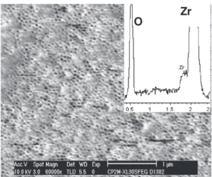
The SEM images (Figs. 1 and 2) show the morphology of the self-organized zirconia nanotubes before and after annealing at 450 °C during 3 h in air. The as-formed porous layer exhibits an uniform and ordered nanotube arrangement. The diameters of the ZrO2 tubes
are around 25–30 nm and the wall thickness is estimated to be approximately 5 nm. The examination of the SEM cross-section (not shown) reveals that the thickness of the ZrO2nt layer is about 2.1μm.
Additionally, the presence of a remaining zirconium layer of about 0.8μm indicates a thickness increase of 11.5% as the thickness of the sputtered zirconium layer was 2.6μm. After the thermal treatment, it can be noticed that the nanoporous matrix does not collapse and is not damaged (nofissure or crack can be seen by SEM). Although a fraction of the tubes are plugged, it is remarkable that the morphology as well as the dimensions of the nanotubes are still preserved.
The corresponding Energy Dispersive X-Ray Spectroscopy (EDS) spectra exhibit two peaks relative to Zr and O. However, as-prepared ZrO2nt shows a peak attributed to the presence of F in the oxide
matrix. Insertion of F is supposed to take place during the anodization process through the decomposition of the F-containing electrolyte leading to the probable formation of a thin ZrF4layer embedding the
external surface of the nanotubes. The formation of such a thin layer has been reported in the case of the electrochemical fabrication of titania nanotubes[25]. Another scenario for the incorporation of F could also be substitution of an oxygen atom by afluorine atom in the oxide bulk near the surface. After annealing, the absence of the peak corresponding to fluorine suggests that it might evaporate as HF during the thermal treatment.
InFig. 3are presented the XRD patterns of the as-prepared and annealed ZrO2nt layers. The pattern for non-annealed sample shows
the presence of a small peak at 2θ=34.9° relative to the residual layer of hexagonal zirconium (JCPDSfile N°005-0665). Four peaks located at 2θ=28.3; 31.5; 34.5 and 51.1 are attributed to the ZrO2monoclinic
phase (JCPDS File No 037-1484) and one peak at 2θ=50.6 to the tetragonal phase (JCPDS File No 050-1089). After annealing, both monoclinic and tetragonal phases are still detected, but two additional intense peaks corresponding to the tetragonal modification appear revealing an increased proportion of tetragonal phase. This result shows that a simple annealing treatment can promote the phase that is known to exhibit good mechanical properties[26].
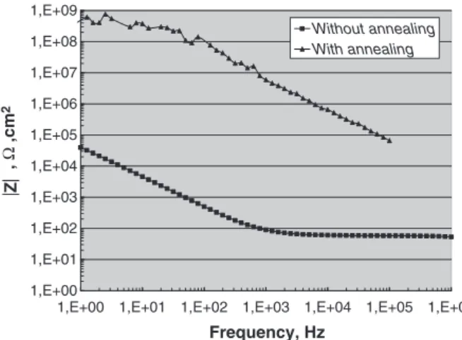
Electrical properties of ZrO2nt before and after annealing were
investigated by Electrochemical Impedance Spectroscopy (Fig. 4). The modulus of the impedance at high frequency is a good approximation of the resistance of the layer. The impedance modulus at low frequency is equal to 1.7 105Ω.cm2for the as-formed ZrO
2nt layer
and equal to 3.108Ω.cm2
after annealing. While the insulating behaviour of the annealed ZrO2nt layer is comparable to pure zirconia
reported in literature, the unexpected semiconductor behaviour observed before annealing can be explained by the presence of fluorine in the structure. Indeed, the insertion of fluorine ions occupying oxygen ion sites is responsible for the generation of excess electrons, as described in Kröger–Vink notation:
OO+ F =OO2+ FO∘ + e′ ð1Þ
Thus,fluoride ions incorporated into zirconia nanotubes have a strong effect on the electrical properties, enhancing n-type conduc-tivity. In contrary, the annealing in oxygen-containing atmosphere removes both F and electrons in ZrO2nt, as can be immediately
concluded by reversing eq.(1). Clearly, the electrical conductivity of ZrO2nt decreases drastically when fluorine is removed from the
structure. This is thefirst evidence of the direct effect of F−upon the
electrical properties of MOxnanotubes prepared by electrochemical
techniques. So far, this effect has been hidden by the intrinsic electrical behaviour of the studied materials; this is especially the case for TiO2nt that remains semiconducting. More generally, the results
presented in this work demonstrate that the electrical properties of MOxnt layers formed by anodization influoride-containing
electro-lytes could be tuned by an appropriate thermal treatment.
O
Zr
F
Fig. 1. SEM observation and EDS analysis of as-formed ZrO2nt.
O
Zr
Fig. 2. SEM observation and EDS analysis of ZrO2nt after annealing.
0 20 40 60 80 100 120 140 26 28 30 32 34 36 38 40 42 44 46 48 50 52 54 56 2θ Counts M T T T M T M M M MM M M M Zr 450 °C - 3h R .T M : monoclinic T : Tetragonal
4. Conclusion
Electrochemical fabrication of zirconia nanotube thin films is described influoride-containing electrolyte. The annealing at 450 °C during 3 h in air does not affect the nanotubular morphology, but changes drastically the structural and electrical properties. Indeed, thermal treatment leads to an increase of the proportion of tetragonal phase, which is the most interesting due to the good mechanical properties. More remarkably, the electrical conductivity of the ZrO2nt
layer can be also turned from semiconductor to insulator afterfluorine removal. This is thefirst evidence of the effect of F on the electrical properties of MOxnanotubes fabricated by anodization of
fluoride-containing electrolytes.
References
[1] L.J. Gauckler, K. Sasaki, Solid State Ionics 75 (1995) 203.
[2] C. Korte, A. Peters, J. Janek, D. Hesse, N. Zakharov, Phys. Chem. Chem. Phys. 10 (31) (2008) 4623.
[3] I. Atribak, I. Such-Basaniez, A. Bueno-Lopez, A. Garcia-Garcia, J. Catal. 250 (1) (2007) 75.
[4] G.-L. Tan, X.-J. Wu, Thin Solid Films 330 (2) (1998) 59.
[5] G. Laukaitis, J. Dudonis, D. Milcius, Thin Solid Films 515 (2) (2006) 678. [6] J.M. Macak, H. Hildebrand, U. Marten-Jahns, P. Schmuki, J. Electroanal. Chem.
621 (2) (2008) 254.
[7] J.M. Macak, P. Schmuki, Electrochim. Acta 52 (3) (2006) 1258.
[8] S. Berger, F. Jakubka, P. Schmuki, Electrochem. Solid St. 12 (7) (2009) K45. [9] J. Zhao, X. Wang, R. Xu, F. Meng, L. Guo, Y. Li, Mater. Lett. 62 (29) (2008) 4428. [10] X. Montero, T. Pauporté, A. Ringuedé, R.-N. Vannier, M. Cassir, J. Power Sources
151 (2005) 85.
[11] J. Zhao, R. Xu, X. Wang, Y. Li, Corros. Sci. 50 (6) (2008) 1593. [12] K. Yasuda, P. Schmuki, Electrochem. Commun. 9 (4) (2007) 615.
[13] S. Berger, F. Jakubka, P. Schmuki, Electrochem. Commun. 10 (12) (2008) 1916. [14] H. Tsuchiya, J.M. Macak, L. Taveira, P. Schmuki, Chem. Phys. Lett. 410 (4–6) (2005)
188.
[15] F. Trivinho-Strixino, F.E.G. Guimarães, E.C. Pereira, Chem. Phys. Lett. 461 (1–3) (2008) 82.
[16] H. Tsuchiya, P. Schmuki, Electrochem. Commun. 6 (11) (2004) 1131.
[17] G.F. Ortiz, I. Hanzu, P. Lavela, J.L. Tirado, P. Knauth, T. Djenizian, J. Mater. Chem. 20 (20) (2010) 4041.
[18] G.F. Ortiz, I. Hanzu, P. Knauth, P. Lavela, J.L. Tirado, T. Djenizian, Electrochim. Acta 54 (17) (2009) 4262.
[19] T. Djenizian, I. Hanzu, Y.D. Premchand, F. Vacandio, P. Knauth, Nanotechnology (2008) 19–20.
[20] F. Vacandio, M. Eyraud, C. Chassigneux, P. Knauth, T. Djenizian, J. Electrochem. Soc. 157 (12) (2010) K279.
[21] Y.D. Premchand, T. Djenizian, F. Vacandio, P. Knauth, Electrochem. Commun. 8 (12) (2006) 1840.
[22] G.F. Ortiz, I. Hanzu, T. Djenizian, P. Lavela, J.L. Tirado, P. Knauth, Chem. Mat. 21 (1) (2009) 63.
[23] G.F. Ortiz, I. Hanzu, P. Knauth, P. Lavela, J.L. Tirado, T. Djenizian, Electrochem. Solid St. 12 (9) (2009) A186.
[24] I. Hanzu, T. Djenizian, P. Knauth, J. Phys. Chem. C 115 (13) (2011) 5989. [25] T. Ruff, R. Hahn, P. Schmuki, Appl. Surf. Sci., in press, Corrected Proof (2011) [26] K. Morita, K. Hiraga, Acta Mater. 50 (5) (2002) 1075.
1,E+00 1,E+01 1,E+02 1,E+03 1,E+04 1,E+05 1,E+06 1,E+07 1,E+08 1,E+09
1,E+00 1,E+01 1,E+02 1,E+03 1,E+04 1,E+05 1,E+06
Frequency, Hz |Z | , Ω ,cm 2 Without annealing With annealing