HAL Id: hal-01166431
https://hal.archives-ouvertes.fr/hal-01166431
Submitted on 22 Jun 2015HAL is a multi-disciplinary open access archive for the deposit and dissemination of sci-entific research documents, whether they are pub-lished or not. The documents may come from teaching and research institutions in France or abroad, or from public or private research centers.
L’archive ouverte pluridisciplinaire HAL, est destinée au dépôt et à la diffusion de documents scientifiques de niveau recherche, publiés ou non, émanant des établissements d’enseignement et de recherche français ou étrangers, des laboratoires publics ou privés.
GaAsPN-based PIN solar cells MBE-grown on GaP
substrates: toward the III-V/Si tandem solar cell
Mickael da Silva, Samy Almosni, C. Cornet, Antoine Létoublon, Christophe
Levallois, Pierre Râle, Laurent Lombez, Jean-François Guillemoles, Olivier
Durand
To cite this version:
Mickael da Silva, Samy Almosni, C. Cornet, Antoine Létoublon, Christophe Levallois, et al.. GaAsPN-based PIN solar cells MBE-grown on GaP substrates: toward the III-V/Si tandem solar cell. SPIE Photonics West - OPTO 2015, Feb 2015, San Francisco, United States. pp.93580H, �10.1117/12.2081376�. �hal-01166431�
GaAsPN-based PIN solar cells MBE-grown on GaP substrates: toward
the III-V/Si tandem solar cell.
M. Da Silva1, S. Almosni1, C. Cornet1, A. Létoublon1, C. Levallois1, P. Rale2, L. Lombez2, J.-F. Guillemoles2, O. Duranda,1
1
Université Européenne de Bretagne, France
INSA, FOTON-OHM, UMR 6082, F-35708 Rennes, France
2
Institut de Recherche et Développement sur l'Energie Photovoltaïque (IRDEP), UMR 7174 - CNRS-EDF-ENSCP, EDF R&D, 6 quai Watier, 78401 Chatou Cedex, France
a
e-mail: olivier.durand@insa-rennes.fr
ABSTRACT
GaAsPN semiconductors are promising material for the elaboration of high efficiencies tandem solar cells on silicon substrates. GaAsPN diluted nitride alloy is studied as the top junction material due to its perfect lattice matching with the Si substrate and its ideal bandgap energy allowing a perfect current matching with the Si bottom cell. We review our recent progress in materials development of the GaAsPN alloy and our recent studies of some of the different building blocks toward the elaboration of a PIN solar cell. A lattice matched (with a GaP(001) substrate, as a first step toward the elaboration on a Si substrate) 1µ m-thick GaAsPN alloy has been grown by MBE. After a post-growth annealing step, this alloy displays a strong absorption around 1.8-1.9 eV, and efficient photoluminescence at room temperature suitable for the elaboration of the targeted solar cell top junction. Early stage GaAsPN PIN solar cells prototypes have been grown on GaP (001) substrates, with 2 different absorber thicknesses (1µ m and 0.3µm). The external quantum efficiencies and the I-V curves show that carriers have been extracted from the GaAsPN alloy absorbers, with an open-circuit voltage of 1.18 V, while displaying low short circuit currents meaning that the GaAsPN structural properties needs a further optimization. A better carrier extraction has been observed with the absorber displaying the smallest thickness, which is coherent with a low carriers diffusion length in our GaAsPN compound. Considering all the pathways for improvement, the efficiency obtained under AM1.5G is however promising.
Keywords: III-V semiconductors; dilute nitride ; molecular beam epitaxy ; multijunction solar cells ; silicon
1. INTRODUCTION
Up to now, the most efficient solar energy conversion systems are monocrystalline multijunction solar cells (MJSC) based on III-V semiconductor materials operating under concentrated sunlight. SOITEC and Fraunhofer Institute have pushed solar cell record to 44.7% for terrestrial applications, with a wafer bonded four-junction GaInP/GaAs//GaInAsP/GaInAs solar cell under concentration of 297 suns 1, and announced very recently a 46% efficiency under concentration of 508 suns, in the SOITEC website. Moreover, a III-V triple junction coherently grown (lattice-matched) onto GaAs substrate has been performed by Solar Junction. This solar cell has shown a 44.4 % efficiency under 942 suns (AM1.5D spectra) 2 due to the use of an 1 eV GaInAsNSb diluted-nitride junction that allow a good current matching with the GaAs and GaInP top junction. The main downside of this approach is the substantial costs of III-V substrates compared to silicon
Invited Paper
Physics, Simulation, and Photonic Engineering of Photovoltaic Devices IV, edited by Alexandre Freundlich, Jean-François Guillemoles, Masakazu Sugiyama, Proc. of SPIE Vol. 9358, 93580H · © 2015 SPIE
CCC code: 0277-786X/15/$18 · doi: 10.1117/12.2081376 Proc. of SPIE Vol. 9358 93580H-1
material which profits from its abundance, mature technology and the wide microelectronics market. Obviously, the integration of III-V junctions on silicon substrate would allow to reach the III-V high efficiencies while benefitting from the advantageous Si substrates cost. This approach would enable to realize a strategic reduction of the solar cells final cost up to 0.25-0.5€/Wp.
A tandem cell with a 1.7 eV III-V top junction on a 1.1 eV monocrystalline Si bottom junction was theoretically studied by Geisz and Friedman, predicting efficiencies higher than 37% under AM 1.5G 3,4,5,6. Still, structural defects such as dislocations would dramatically reduce the performance of such a structure by trapping the charge carriers. It is thus necessary to perform a lattice matched growth onto silicon.Our work consists of the development of a lattice matched III-V/c-Si tandem cell. We report here our results on the growth and the technological processing of the III-V top solar subcell preliminary grown on GaP(001). First, we describe the growth and the technologic process of this top III-V subcell. Then, we report our recent results about this III-V cell.
2. EXPERIMENTAL DETAILS ON THE SOLAR CELL FABRICATION
In order to develop low cost and high efficiency tandem solar cells on c-Si substrates, our group have oriented its research toward a lattice-matched GaAsPN based top cell grown on GaP(001), as a first stage towards the tandem cell development itself. Indeed, GaP is the III-V compound with the closest lattice parameter to Si, with a lattice mismatch around 0.4%, but its wide bandgap (2.2 eV) makes it transparent for most of the solar spectrum. Moreover, GaP has an indirect band gap, which leads to low performances when used as an absorber. The introduction of small amount of As (typically 10%) and N (typically 2%) in GaP, leads to a pseudo-direct band gap material (GaAsPN), while maintaining a perfect lattice matching with GaP(001) 7. Moreover, the incorporation of a low amount of N enables to lower the bandgap towards the theoretical ideal value of 1.7 eV, thanks to a large bowing effect, property leading to a huge electronic bandgap variation with respect to a small nitrogen incorporation 8,9,10. We have designed this top cell as a PIN diode - composed of an unintentionally doped GaAsPN absorber under a p-doped GaP layer - grown by molecular beam epitaxy (MBE) on a n-doped GaP substrate. The p and n-type doping are obtained during the growth thanks to beryllium and silicon cells respectively. We also report our results about ohmic contacts deposition on both p and n-type GaP substrates.
2.1 Growth and post growth treatment.
The III-V top cell is grown in a RIBER MBE chamber on a GaP(001) substrate. The group III elements, such as Ga, are emitted by conventional Knudsen effusion cells from pure metal solid sources. The V elements, like P and As, are supplied by valved-cracker cells by heating solid sources. The basis pressure in the chamber is about 10-11 Torr while the growth pressure attains 10-7-10-5 Torr. To grow the dilute nitride compound, the atomic N is produced by a valved Addon RF plasma cell, designed to avoid any ion irradiation of the sample during the growth,11 is used.
Based on the work of Harris et al. (2007) on the GaInAsN dilute-nitride compounds, a growth at low temperature (480°C) has been chosen in order to minimize the point defects density and the phase separation known to occur in non-optimized dilute-nitride alloys growth 12,13. It has also been found out that lowering the growth rate raises the nitrogen incorporation 12. This provides a major asset for the controllability and the reproducibility of these dilute nitride compounds.
In dilute-nitride materials, post-growth treatments, such as annealing, is highly required to obtain the optimal optical properties for the targeted applications 14. In particular, it has been shown that an annealing step after the growth reduces the alloy fluctuations and suppresses some of the remaining point defects in the dilute nitride compounds 15 Such a process drastically improves the optical properties of the absorber 12,16. Therefore, a first stage post growth annealing study (not shown here), has been performed. In the following,
the structures have been annealed at 800°C for 5 min which has been found to dramatically improve the optical properties of the diluted nitride compounds.
2.2 GaP doping
The targeted structure is a PIN GaP/GaAsPN/GaP junction grown onto a GaP substrate. Therefore, the doping of GaP has been studied. P and n dopings of GaP are respectively obtained using solid Be and Si sources sublimated in Knudsen cells in the MBE chamber. C-V measurements performed on doped GaP layers grown on GaP substrates have been performed and allowed to draw the Arrhenius plots of each doping cell as represented in figures 1 and 2. Results on InP samples are shown for comparison.
Fig. 1: Evolution of the n-type doping level for GaP and InP growths as a function of the reverse of the dopant cell temperature.
Fig. 2: Evolution of the p-type doping level for GaP and InP growths as a function of the reverse of the dopant cell temperature.
One can notice that the doping species modify the slope of the Arrhenius plot while the nature of the grown material does not have any influence. On figure 1, a former Si cell, with a conical geometry, is compared to a recently installed one, with a rounded back (whose purpose was the obtaining of a high doping level). As expected, this new cell allows higher doping levels than the former one, which enables us to achieve high doping levels – higher than 1019 cm-3 - for both p and n doping. These values are suitable for the growth of operating PIN solar cells and particularly for the development of an optimal tunnel junction (TJ) 17. Indeed, both the top and bottom subcells of the tandem GaAsPN/Si double-junction solar cell will be electrically connected with a TJ.
2.3 Ohmic contacts on GaP
The elaboration of low resistance ohmic contacts is a key issue for an efficient collection of the photo-generated carriers. Contacts with a too high resistance would result in additional effects on the total current in the device, making the cell efficiency drop dramatically. The requirements for ideal ohmic contacts are linear and symmetrical I-V characteristic with a reliable and reproducible behavior. An optimized annealing step is necessary to ensure the mechanical stability of the metallic alloys. For n-type GaP substrate, we have referred to the work of Peternai et al. (2003) and have chosen to use a Ni/Au/Ge alloy 18, annealed at 530°C. This structure has shown a symmetrical ohmic contact characteristic with a good reproducibility and mechanical stability. In addition, we have obtained a low contact resistivity of 10-5 Ω.cm² on a n-type GaP substrate (n~1018 cm-3). Regarding the p-doped GaP, the use of a Pd/Au/Zn alloy has been reported to be a good choice
19,20
. After an annealing of 550°C, we have been able to notice again an adequate ohmic behavior for this contact, with a low resistivity of 10-5 Ω.cm² on a p-type (p~1018 cm-3) GaP substrate.
2.4 PIN solar cells development
Fig. 3: PIN/GaP solar cells development flowchart.
In order to develop the top junction, GaP/GaAsPN PIN diodes have been grown on a n-type GaP(001) substrate. The structures consists of a p-doped (Be doped, 1.1018 cm-3) GaP window layer grown on a GaAsPN absorber, itself grown on a n-doped (Si doped, 1.1018 cm-3) GaP bottom layer. The ohmic contacts on the front and back surfaces have been described previously. The front contact consists of a 5*5 mm² grid with 10 µm large fingers each spaced by 300 µm. The structure has been annealed at 800°C for 5 min in order to improve the optical properties of the diluted nitride compound. A front-fingered contact is deposited through a liftoff procedure, employing photolithography, after an oxide removal from the surface, done in a 5% HF solution. The fingers, which size is 2.5 mm * 5 µm, are spaced from each other of 300 µm (fig.3). The busbar size is 2.5 mm * 0.5 mm. the Pd/Au/Zn-based front contact is then deposited. All the photolithography steps have been performed in soft contact allowing line space resolution of 5 µm. After the lift-off process, the front sample surface is protected using photoresist and the substrate is thinned. Indeed, substrate thinning, using mechanical polishing, from 400 µm to 200 µm is important to improve the solar cell efficiency. We have observed that solar cells with a thinned substrate present an increase of the open-circuit voltage (Voc),
short circuit current (Jsc) and fill factor (FF), leading to a significant improvement of their overall yields. This
behavior has been attributed to the presence of detrimental impurities inside the GaP substrate, such as isoelectronic nearest-neighbor Zn-O pair known to act as recombination centers 21,22.
After the mechanical polishing, a SiN layer is deposited by plasma enhanced chemical vapor deposition (PECVD) at 300°C and a second photolithography step is done. Then, the SiN layer is etched by a reactive
ion etching (RIE) process using SF6 gas. This dry etching step is then followed by a chemical etching to create 3 mm x 2.5 mm mesas in order to ensure an electrical insulation between the front side and the back side of the solar cell. A hard SiN dielectric mask is used to protect the contact zone and the active area. After the dry etching, the SiN layer and remaining photoresist are removed. The sample is then dipped 30s in a 5% HF chemical solution, dried and the Ni/Au/Ge contact is deposed using an electron gun on the back side of the sample. Finally a last annealing step is performed at 540°C 3 min to alloy both contacts at the same time.
3. EARLY STAGE RESULTS ON PIN DIODES GROWN ON GAP SUBSTRATE
We introduce here our early-stage results on PIN GaAsPN based solar cells development. The performances of each diode are discussed, as well as some routes for possible improvements. The performances evaluation is based on external quantum efficiency (EQE) measurements under AM1.5G. Quantum efficiency refers to the ratio between the number of incident photons and the number of collected charge carriers from the device. EQE does not take into account the amount of photons reflected or transmitted by the structure, thus this experiment also includes the power losses due to absorption limitations (lack of anti-reflection coating for instance). I-V curves showing the Jsc, the Voc, the FF and the efficiency of every cell have also been plotted.
3.1 Study of a 1 µm-thick absorber grown on a GaP(001) substrate
68.6 68.7 68.8 68.9 69.0 69.1 69.2
10
-410
-310
-210
-110
0In
te
n
si
ty
(
a
rb
.u
n
it
)
2
θθθθ
(degrees)
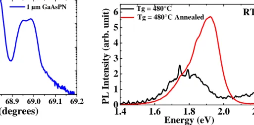
1 µm GaAsPNFig. 4: XRD diagram performed around the (004) GaP reflection of a 1 µ m thick GaAsPN layer grown quasi lattice matched with the GaP substrate.
Fig. 5: RT PL spectra of a 1 µ m thick GaAsPN layer grown on a GaP substrate, before annealing (black line) and annealed at 800°C during 5 min (red line).
In a first step, a 1 µm-thick absorber has been used to ensure an optimal absorption of the incident light inside the absorber. This thickness has been theoretically determined after a first simulation of the PIN structure using SILVACO software. The 1 µm-thick GaAsPN layer, with an estimated composition of GaAs0.10P0.88N0.02 (from X-ray diffraction experiments on a GaPN compound grown in the same conditions
and taking into account the As incorporation), displays no structural relaxation due to its low mismatch (0.07%) with the GaP substrate, as measured through X-ray diffraction. However, a very small peak splitting has been observed (fig.4). This effect could be related to a small composition fluctuation, as already observed in the GaInAsN material and which has been attributed to a “phase separation” 12. Moreover, an optical gap of around 1.8 eV has been measured through Room Temperature Photoluminescence (PL) measurement (fig.5).
1.4
1.6
1.8
2.0
2.2
0
1
2
3
4
5
6
Tg = 480°C AnnealedTg = 480°CRT
P
L
I
n
te
n
si
ty
(
a
rb
.
u
n
it
)
Energy (eV)
GaP(p+) 250 nm GaAsPN(i) 1 µm GaP(n +) 300 nm GaP(n +) 200 µm substrate
One can observed a low energy tail in the PL spectra, which is typical of the dilute-nitrides materials and usually attributed to local density of states due to alloy fluctuations effects from nitrogen clusters 14,23.
3.2 PIN diode with a 1µm thick GaAsPN absorber
Fig. 6: Structure of the GaP/GaAsPN/GaP PIN diode (sample 1) with a 1µ m thick absorber.
Our first design for the development of a GaP/GaAsPN/GaP PIN diode is described in figure 6. This sample is labelled sample 1 in the following. The EQE and I-V curves are shown in figures 8. The EQE shows an encouraging response at low energy, around 30%, and a weak response at higher energy. The last effect has been attributed to the top 250-nm thick GaP highly doped layer absorption. I-V characteristics under AM1.5G illumination condition has been measured (fig 8). While the measured open-circuit voltage Voc is 1.18 V, the
FF of 50% and the efficiency of 1.6% are limited by a small short-circuit current Jsc of 2.8 mA/cm², far from
the state-of-the art 4. The I-V curve behavior seems to indicate a low carriers extraction from the solar cell. One can assume that the absorber thickness is too large compared to the diffusion length of the carriers in this material 24 whose structural properties has to be optimised. Measurement of the carriers diffusion length in our GaAsPN compounds will be done in a forthcoming study. Therefore, we aimed to reduce this thickness to improve the solar cell properties.
3.3 PIN diode with a 0.3µm thick GaAsPN absorber
Fig. 7: Structure of the GaP/GaAsPN/GaP PIN diode (sample 2) with a 300 nm thick absorber.
As depicted in figure 7,both the GaAsPN absorber and the GaP (p+) top layer have been thinned in order to, first, obtain a better carrier collection, while lowering the light absorption. Figure 8 shows the EQE results of each reported sample. Compared to the previous sample, the response at low energy of sample 2 is close,
while lower, to the one obtained with sample 1, which shows that the carrier collection has been improved, taking into account the smaller thickness. The larger response at higher energy has been attributed to the lower light absorption in the top GaP highly doped layer, much thinner that in sample 1.This is in agreement with our assumption of a low carriers collection in our GaAsPN absorber. Concerning the I-V curve under AM1.5G illumination conditions, this cell has displayed a Jsc of 3.8 mA/cm², larger than in sample 1. While
Voc is slightly lower at 0.88 V, which has not been understood so far, a remarkable fill factor of 71% has been
measured. Finally, an encouraging 2.3% efficiency has been obtained 25.
3.4 Influence of the growth rate
Sample 3 has exactly the same design than sample 2. The only change consisted in a lower growth rate. Indeed, as mentioned previously, it has been observed that the lower the growth rate, the higher is the N content 12, so that we expect to obtain a higher nitrogen incorporation in the GaAsPN compound and, therefore a lower GaAsPN bandgap, much closer to the expected 1.7 eV. Indeed, the EQE results in a lower cut-off at low energy, as expected, which is accompanied by a higher Jsc (4.1 mA/cm²) in the I-V under
illumination. Voc is unchanged but a resistive effect shown by the shape of the I-V curve at low voltage results
in lower fill factor (49%) and efficiency (1.75%). Still, this sample remains interesting since the electric current in the final tandem cell structure will be limited by the weakest current of the subcells taken alone. In other words, it might be appealing to slightly sacrifice the cell efficiency so as to maintain the current matching in the whole device. Moreover, these new growth parameters imply a forthcoming optimisation of the overall growth, as well as post-growth annealing, along with an experimental study of different absorber thicknesses between 0.3µm and 1µm.
2.0
2.5
3.0
3.5
4.0
0
5
10
15
20
25
30
35
40
45
50
E
x
te
rn
a
l
Q
E
E (eV)
sample 1 sample 2 sample 3-1.0
-0.5
0.0
0.5
1.0
-4
-2
0
2
4
C
u
rr
en
t
d
en
si
ty
(
m
A
/c
m
²)
Bias (V)
sample 1 sample 2 sample 3Fig. 8: EQE versus energy (left) and I-V curves under illumination (AM1.5G) (right) for the three GaP/GaAsPN/GaP PIN diodes.
3.5 Conclusion
Those early stage results have to be compared to the state-of-the-art device developed by Geisz et al. in 2002. Their GaP/GaAsPN(600nm)/GaP PIN diode reached the efficiency of 3.8% with a 5.8 mA/cm² Jsc a 1.1V Voc
(Eg = 1.88eV) and a FF of 60% 4. Our approach is promising considering all the possible routes for improvement. Mainly, sample 2 with a 300 nm thick GaAsPN absorber displayed a promising η = 2.3%, with a FF of 70%. Its main shortcoming comes from its weak current collection which shows the necessity to optimize the cell architecture and the GaAsPN structural properties.
4. CONCLUSION
We have reported first-stage-stage results on GaP/GaAsPN/GaP PIN solar cells grown by MBE on GaP(001) substrates, toward the development of a III-V/Si tandem solar cell. Moreover, we have achieved the development of high doping levels of the GaP layers, suitable for the development of an efficient TJ, and suitable quality ohmic contacts. Our best efficiency result (2.3%) has been obtained with a 300 nm-thick GaAsPN absorber, while 1 µm is required for an optimal light absorption. Indeed, GaAsPN is an emerging material not fully optimized so far. However, an EQE around 30% and FF of 70% have been demonstrated, and a VOC of 1.18 V has been reached. Moreover, much progress has been realized in the comprehension of
the influence of growth and annealing parameters and the control of the GaAsPN composition. Nevertheless, there is yet a room for improvement of the structural characteristics of the material, and, therefore on its optical properties. Moreover, we obtained these results despite the lack of any anti-reflective layers and passivation coating. In addition to further optimizations, our forthcoming work will include the study of these coatings and the development of a high performance TJ for the electrical connection between both subcells17. Finally, the III-V top cell will be grown on the Si bottom one to complete the tandem cell. In this regard, our group have also developed a strategy to grow GaP defect-free layers on silicon, avoiding most of the local chemistry mismatch at the GaP/Si interface such as anti-phase domains and microtwins which are typical of epitaxies of polar materials on non-polar ones26–31.
Acknowledgments: This work was supported by the French ANR, project MENHIRS (grant
N°ANR-2011-PRGE-007-0).
REFERENCES
[1] Dimroth, F., Grave, M., Beutel, P., Fiedeler, U., Karcher, C., Tibbits, T. N. D., Oliva, E., Siefer, G., Schachtner, M., et al., “Wafer bonded four-junction GaInP/GaAs//GaInAsP/GaInAs concentrator solar cells with 44.7% efficiency,” Prog. Photovolt. Res. Appl. 22(3), 277–282 (2014).
[2] Derkacs, D., Jones-Albertus, R., Suarez, F.., Fidaner, O., “Lattice-matched multijunction solar cells employing a 1 eV GaInNAsSb bottom cell,” J. Photonics Energy 2(1), 021805–1 (2012).
[3] Kurtz, S. R., Faine, P.., Olson, J. M., “Modeling of two‐junction, series‐connected tandem solar cells using top‐cell thickness as an adjustable parameter,” J. Appl. Phys. 68(4), 1890–1895 (1990). [4] Geisz, J. F., Olson, J. M., Friedman, D. J., Jones, K. M., Reedy, R. C.., Romero, M. J.,
“Lattice-matched GaNPAs-on-silicon tandem solar cells,” Conf. Rec. Thirty-First IEEE Photovolt. Spec. Conf. 2005, 695–698 (2005).
[5] Geisz, J. F.., Friedman, D. J., “III–N–V semiconductors for solar photovoltaic applications,” Semicond. Sci. Technol. 17(8), 769 (2002).
[6] Geisz, J. F., Friedman, D. J.., Kurtz, S., “GaNPAs solar cells lattice-matched to GaP,” Conf. Rec. Twenty-Ninth IEEE Photovolt. Spec. Conf. 2002, 864–867 (2002).
[7] Chamings, J., Adams, A. R., Sweeney, S. J., Kunert, B., Volz, K.., Stolz, W., “Temperature dependence and physical properties of Ga(NAsP)/GaP semiconductor lasers,” Appl. Phys. Lett.
93(10), 101108 (2008).
[8] Shan, W., Walukiewicz, W., Yu, K. M., Wu, J., Iii, J. W. A., Haller, E. E., Xin, H. P.., Tu, C. W., “Nature of the fundamental band gap in GaNxP1−x alloys,” Appl. Phys. Lett. 76(22), 3251–3253 (2000).
[9] Robert, C., Bondi, A., Thanh, T. N., Even, J., Cornet, C., Durand, O., Burin, J. P., Jancu, J. M., Guo, W., et al., “Room temperature operation of GaAsP(N)/GaP(N) quantum well based light-emitting diodes: Effect of the incorporation of nitrogen,” Appl. Phys. Lett. 98(25), 251110 (2011).
[10] Xin, H. P., Tu, C. W., Zhang, Y.., Mascarenhas, A., “Effects of nitrogen on the band structure of GaNxP1−x alloys,” Appl. Phys. Lett. 76(10), 1267–1269 (2000).
[11] Kuyyalil, J., Nguyen Thanh, T., Quinci, T., Almosni, S., Létoublon, A., Rohel, T., Bertru, N., Le Corre, A., Durand, O., et al., “Nitrogen–phosphorus competition in the molecular beam epitaxy of GaPN,” J. Cryst. Growth 377, 17–21 (2013).
[12] Harris, J. S., Kudrawiec, R., Yuen, H. B., Bank, S. R., Bae, H. P., Wistey, M. A., Jackrel, D., Pickett, E. R., Sarmiento, T., et al., “Development of GaInNAsSb alloys: Growth, band structure, optical properties and applications,” Phys. Status Solidi B 244(8), 2707–2729 (2007).
[13] Aho, A., Polojärvi, V., Korpijärvi, V.-M., Salmi, J., Tukiainen, A., Laukkanen, P.., Guina, M., “Composition dependent growth dynamics in molecular beam epitaxy of GaInNAs solar cells,” Sol. Energy Mater. Sol. Cells 124, 150–158 (2014).
[14] Utsumi, A., Yonezu, H., Furukawa, Y., Momose, K.., Kuroki, K., “Increase in luminescence efficiency of GaPN layers by thermal annealing,” Phys. Status Solidi C(7), 2741–2744 (2003).
[15] Jussila, H., Yu, K. M., Kujala, J., Tuomisto, F., Nagarajan, S., Lemettinen, J., Huhtio, T., Tuomi, T. O., Lipsanen, H., et al., “Substitutionality of nitrogen atoms and formation of nitrogen complexes and point defects in GaPN alloys,” J. Phys. Appl. Phys. 47(7), 075106 (2014).
[16] Aho, A., Tukiainen, A., Polojärvi, V., Salmi, J.., Guina, M., “High current generation in dilute nitride solar cells grown by molecular beam epitaxy,” Proc. SPIE 8620, Physics, Simulation, and Photonic Engineering of Photovoltaic Devices II, 86201I – 86201I – 6 (2013)
[17] Rolland, A., Pedesseau, L., Even, J., Almosni, S., Robert, C., Cornet, C., Jancu, J. M., Benhlal, J., Durand, O., et al., “Design of a lattice-matched III–V–N/Si photovoltaic tandem cell monolithically integrated on silicon substrate,” Opt. Quantum Electron. 46(10), 1397–1403 (2014).
[18] Peternai, L., Jakabovič, J.., Michalka, M., “Ohmic contacts to n–and p–type GaP,” 9th Int. Workshop APCOM, 157–160 (2003).
[19] Baojun, L., Enke, L.., Fujia, Z., “Pd/Zn/Pd ohmic contacts to p-type GaP,” Solid-State Electron. 41(6), 917–920 (1997).
[20] Zhang, F., Zhang, D., Li, B., Liu, E., Liu, F.., Gan, R., “Pb/Zn/Pd ohmic contacts to p-GaP,” Mater. Sci. Eng. B 48(3), 198–201 (1997).
[21] Montgomery, K. H., Allen, C. R., Wildeson, I. H., Jeon, J.-H., Ramdas, A. K.., Woodall, J. M., “Gettered GaP Substrates for Improved Multijunction Solar Cell Devices,” J. Electron. Mater. 40(6), 1457–1460 (2011).
[22] Gershenzon, M.., Mikulyak, R. M., “RADIATIVE PAIR RECOMBINATION AND SURFACE RECOMBINATION IN GaP PHOTOLUMINESCENCE,” Appl. Phys. Lett. 8(10), 245–247 (1966). [23] Kent, P. R. C.., Zunger, A., “Theory of electronic structure evolution in GaAsN and GaPN alloys,”
Phys. Rev. B 64(11), 115208 (2001).
[24] Fahy, S.., O’Reilly, E. P., “Intrinsic limits on electron mobility in dilute nitride semiconductors,” Appl. Phys. Lett. 83(18), 3731–3733 (2003).
[25] Durand, O., Almosni, S., Ping Wang, Y., Cornet, C., Létoublon, A., Robert, C., Levallois, C., Pedesseau, L., Rolland, A., et al., “Monolithic Integration of Diluted-Nitride III–V-N Compounds on Silicon Substrates: Toward the III–V/Si Concentrated Photovoltaics,” Energy Harvest. Syst. , 147–156 (2014).
[26] Matthews, J. W.., Blakeslee, A. E., “Defects in epitaxial multilayers: I. Misfit dislocations,” J. Cryst. Growth 27, 118–125 (1974).
[27] Grassman, T. J., Brenner, M. R., Rajagopalan, S., Unocic, R., Dehoff, R., Mills, M., Fraser, H.., Ringel, S. A., “Control and elimination of nucleation-related defects in GaP/Si(001) heteroepitaxy,” Appl. Phys. Lett. 94(23), 232106 (2009).
[28] Létoublon, A., Guo, W., Cornet, C., Boulle, A., Véron, M., Bondi, A., Durand, O., Rohel, T., Dehaese, O., et al., “X-ray study of antiphase domains and their stability in MBE grown GaP on Si,” J. Cryst. Growth 323(1), 409–412 (2011).
[29] Thanh, T. N., Robert, C., Guo, W., Létoublon, A., Cornet, C., Elias, G., Ponchet, A., Rohel, T., Bertru, N., et al., “Structural and optical analyses of GaP/Si and (GaAsPN/GaPN)/GaP/Si nanolayers for integrated photonics on silicon,” J. Appl. Phys. 112(5), 053521 (2012).
[30] Quinci, T., Kuyyalil, J., Thanh, T. N., Wang, Y. P., Almosni, S., Létoublon, A., Rohel, T., Tavernier, K., Chevalier, N., et al., “Defects limitation in epitaxial GaP on bistepped Si surface using UHVCVD– MBE growth cluster,” J. Cryst. Growth 380, 157–162 (2013).
[31] Nguyen Thanh, T., Robert, C., Létoublon, A., Cornet, C., Quinci, T., Giudicelli, E., Almosni, S., Boudet, N., Ponchet, A., et al., “Synchrotron X-ray diffraction analysis for quantitative defect evaluation in GaP/Si nanolayers,” Thin Solid Films 541, 36–40 (2013).