HAL Id: hal-00089420
https://hal.archives-ouvertes.fr/hal-00089420
Submitted on 18 Aug 2006HAL is a multi-disciplinary open access archive for the deposit and dissemination of sci-entific research documents, whether they are pub-lished or not. The documents may come from teaching and research institutions in France or abroad, or from public or private research centers.
L’archive ouverte pluridisciplinaire HAL, est destinée au dépôt et à la diffusion de documents scientifiques de niveau recherche, publiés ou non, émanant des établissements d’enseignement et de recherche français ou étrangers, des laboratoires publics ou privés.
Software radio and dynamic reconfiguration on a
DSP/FPGA platform
Jean-Philippe Delahaye, Guy Gogniat, Christian Roland, Pierre Bomel
To cite this version:
Jean-Philippe Delahaye, Guy Gogniat, Christian Roland, Pierre Bomel. Software radio and dynamic reconfiguration on a DSP/FPGA platform. 3rd Karlsruhe Workshop on Software Radios, 2004, France. pp.XX. �hal-00089420�
Abstract-- This paper discusses the implementation of
modulation chains for multi-standards communication on a dynamically and partially reconfigurable heterogeneous platform. Implementation results highlight the benefit of considering a DSP/FPGA platform instead of a multi-DSP platform since the FPGA supports efficiently intensive computation components which reduces the DSP load. Furthermore partial dynamic reconfiguration increases overall performances compared to total dynamic reconfiguration since there is 45% of bitstream size reduction which leads to a 45% decrease of the whole reconfiguration time. The implementation of modulation chains for multi-standards communication proves the availability of new technology to support efficiently Software Defined Radio.
Index terms-- HW/SW CoDesign, baseband data
processing, partial dynamic reconfiguration, Software Defined Radio
I. INTRODUCTION
In this paper we present a wireless reconfigurable architecture for Universal Terminal. The idea of a re-configurable terminal first appeared in the military area. In fact, the need for reconfiguration appeared very soon in the 70’s, with for example the first equipment called “SPEAKeasy” [1]. This concept became popular in the civil telecommunications area in the 90’s, thanks mainly to the work of J. Mitola [2].
There is now a growing interest in reconfigurable terminals. This sector, whatever the technique used to offer this reconfigurability, is one of the fastest growing sectors in the telecommunications industry. But it should be noted that this topic is also a logic consequence of the performance increase of DSPs and FPGAs and is in line with the historical evolution of the replacement of analogical part by digital part. DSPs and FPGAs provide the flexibility and the computation power required to perform digital front end. FPGAs enable to take advantage of computation parallelism to achieve high performance with moderate power consumption. Furthermore FPGAs can be reconfigured in order to provide multi standards/services terminals.
In particular one can imagine a given device that should support several digital mobile telephony services, digital broadcasting services, and/or digital data transfer services by just changing its software. Current devices can provide
only one type of service due to limitations (inflexibility) mainly imposed by their analog technology parts. This explains the growing interest in multi-mode terminals performed thanks to Software Defined Radio (SDR) techniques.
Software Defined Radio basically refers to a set of techniques that permit the reconfiguration of a communication system without the need to change any hardware system element. The goal of Software Defined Radio is to produce communication devices capable of supporting several different services. These terminals must adapt their hardware in function of the wireless networks such as GSM, IS95, PDC, DECT, PHS and the future UMTS. In addition they should take into account wireless standard like RLAN and Hiperlan, as well as in the broadcasting area like DAB and DVB-T.
The very important point is the fact that this adaptation should be dynamic, more or less in real time, in order to take into account all the variations.
The contribution of this work is to prove the feasibility of dynamic and partial reconfiguration on a heterogeneous platform composed of one DSP TI C6201 and a Xilinx Virtex 1000E FPGA. To perform this implementation we have focussed on the application, the platform and the design flow, which is an essential issue in order to make the Software Defined Radio approach achievable.
The paper is arranged as follows: Section 2 reviews previous work related to Software Defined Radio. Section 3 focuses on FPGA technology and particularly on reconfiguration requirements. Section 4 looks at the details of the experimentation platform used to perform this study. This provides the necessary background for an appreciation of the design flow and the case study that are described in sections 5 and 6. Section 7 presents future work and concludes the paper.
II. RELATED WORK
This section presents the concept of reconfiguration in both domains application and architecture involved in the Software Defined Radio paradigm.
The concept of Software Defined Radio is closely related to the need of further flexibility imperative for future terminals. As explain by Polydoros et al. [3] the flexibility of a terminal involves the system to be adaptive and reconfigurable. The system is adaptive if it can respond to
S
OFTWARE
R
ADIO AND
D
YNAMIC
R
ECONFIGURATION ON A
DSP/FPGA
PLATFORM
J. P. Delahaye1, G. Gogniat2, C. Roland2, P. Bomel2
1IETR/Supelec - Campus de Rennes, Av. de la Boulais, BP 81127 35511 Cesson-sévigné France
2Laboratoire LESTER – Université de Bretagne Sud - CNRS FRE 2734 Centre de Recherche, BP 92116, 56321 Lorient France { pierre.bomel | guy.gogniat | christian.roland}@univ-ubs.fr
application changes by properly altering the numerical value of a set of parameter [4]. It is reconfigurable if it can be rearranged, at a procedural, structural or architectural level.
As many standard will be accessible in a Universal Terminal, search of common functions or operators [5] (e.g. parameterisation) has many interest. It is possible for example to design every modulator (OFDM, QPSK, GMSK) with one filter bank and to reconfigure just a part of the physical layer. This search will concern processing of the whole protocol stack of every standard and the major interest of the parametrisation is to decrease the size of the software to be downloaded (locally or over the air) to partially reconfigure the standard.
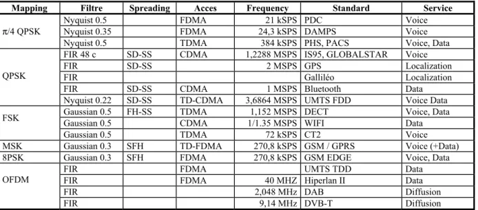
We present in Table 1 the main characteristics of widespread standards for physical layer functions since this layer corresponds to the most critical one in term of computation power and required throughput. Hence the partial reconfiguration of this layer is particularly important and corresponds to an interesting candidate for implementation on FPGAs.
Obviously, to perform Software Defined Radio reconfiguration standards must exist in a same geographical area. For example DVB-T (Europe) and DAMPS (USA) are not available together.
Standards concern different classes of services hence reconfiguration of a terminal during roaming (to change from one network to another one) has to be done or not in
real time, it depends if service continuity is required or not. Furthermore, partial reconfiguration can be performed even if service continuity is not required, in that case the objective is to enhance software performance (size and download time). Table 2 illustrates these concepts with different standards and services.
It is important to note that reconfiguration may conduct to significant changes in the terminal, which may lead to an important timing overhead. As real time is an important issue for Software Defined Radio terminals a thorough analysis of timing characteristics is required. Hard real time constraint is generally required to manage performance enhancement, bug-fixing or standard roaming (e.g., GSM to EDGE) when the reconfiguration time is critical in order to guaranty services continuity. In the case of soft real time constraint, the reconfiguration time is not a critical issue since the utilisation of the system is stopped while the reconfiguration is performed. This is typically the case when changing from one standard to another standard (e.g., GSM to Broadcast). In that case there is no necessity to guaranty service continuity.
To support reconfiguration, different platforms can be considered. In the following we only address embedded platforms since this paper focuses on the concept of universal terminal. Right now most of the studies have focussed on software platform composed of several processors (typically, one RISC and several DSPs). For
Mapping Filtre Spreading Acces Frequency Standard Service
Nyquist 0.5 FDMA 21 kSPS PDC Voice
Nyquist 0.35 FDMA 24,3 kSPS DAMPS Voice
π/4 QPSK
Nyquist 0.5 TDMA 384 kSPS PHS, PACS Voice, Data
FIR 48 c SD-SS CDMA 1,2288 MSPS IS95, GLOBALSTAR Voice
FIR SD-SS 2 MSPS GPS Localization
FIR Galliléo Localization
FIR SD-SS CDMA 1 MSPS Bluetooth Data
QPSK
Nyquist 0.22 SD-SS TD-CDMA 3,6864 MSPS UMTS FDD Voice Data Gaussian 0.5 FH-SS TDMA 1,152 MSPS DECT Voice, Data
Gaussian 0.5 CDMA 1/1.35 MSPS WIFI Data
FSK
Gaussian 0.5 TDMA 72 kSPS CT2 Voice
MSK Gaussian 0.3 SFH TD-FDMA 270,8 kSPS GSM / GPRS Voice (+Data)
8PSK Gaussian 0.3 SFH FDMA 270,8 kSPS GSM EDGE Voice, Data
FIR FDMA UMTS TDD Data
FIR FDMA 40 MHZ Hiperlan II Data
FIR 2,048 MHz DAB Diffusion
OFDM
FIR 9,14 MHz DVB-T Diffusion
Table 1. Physical layer Functions per standard
Service continuity
Partial / Global
Sandard 1 Santard 2 Comments Service
Partial DAB (DVB-T) DVB-T (DAB) OFDM (carriers/SF) Diffusion ⇒ diffusion
Global FM DAB Analog / OFDM Diffusion ⇒ diffusion
No
GSM DVB-T GMSK / OFDM voice ⇒ Diffusion
Partial GSM (DECT) DECT (GSM) GMSK / QPSK V outdoor ⇒ V home
Partial GSM EDGE (GPRS) GMSK / 8PSK Voice (Data)
Partial PHS GSM QPSK / GMSK V home ⇒ V outdoor
Partial IS95 UMTS FDD CDMA / TD-CDMA Voice (Data) Global GSM UMTS FDD Modulation and Acces Voice (Data) Yes
Global GSM Bluetooth Modulation and Acces V outdoor ⇒ V rlan
example in [6] a platform based on four TIC6201 DSP is used to realise some software upgrades. They have performed a bug-fixing scenario in the case of an EDGE receiver using a software component-based approach. Reconfiguration can also be carried out on hardware platform composed of reconfigurable architectures. Many studies have been done to propose coarse grain reconfigurab le architectures. These architectures are based on a datapath that can be adapted in order to optimise the execution performance of the application. In [7] Srikanteswara et al. propose an overview of configurable computing machines for Software Defined Radio handsets. Coarse grain reconfigurable architectures [8] are mainly considered as hardware accelerators and are generally under the control of a processor (DSP or RISC).
Another category of architecture is now providing very interesting mechanisms to perform dynamic reconfiguration. Cummings and Haruyama first described benefits of the introduction of SRAM Field Programmable Gate Array architectures (FPGA) in Software Defined Radio [9]. Now FPGAs offer very high-density integration and some devices support dynamic partial reconfiguration. Dynamic reconfiguration enables to configure during the application execution some parts of the architecture in order to enhance performance or to reduce power consumption. In the following section we focus on this last solution since this new feature will be mandatory [3] to enhance the flexibility of the physical layer processing.
III. RECONFIGURATION AND FPGA
The implementation of one or several applications can be done in different ways using a single FPGA. The reconfiguration scenarios depend on the application characteristics and on the reconfiguration abilities of the FPGA.
Before going more in the details of reconfiguration scenarios, several points must be clearly defined. The reconfiguration of a FPGA is dependent of what it is called the reconfiguration memory (RM), which corresponds to an array of configuration points (typically SRAM cell). This reconfiguration memory can be programmed through several mechanisms: if the structure of the RM is based on an array of columns the reconfiguration can only be done column by column (this is the case for FPGAs like Xilinx Virtex used in that study). In the following we call this type of RM, 1D-array reconfiguration. It is important to note that with this kind of component only a whole column can be reconfigured and not a part of it. If the structure of the RM is like a true memory where each reconfiguration point can be accessed independently we call it, 2D-array reconfiguration. In that case there is no limitation on the reconfiguration approach.
Another important definition is related to partial and full (also called total or global) reconfiguration. Partial reconfiguration means that only a part of the FPGA is reconfigured (several columns in the case of 1D-array memory and a part of the FPGA for 2D-array memory). Full reconfiguration means that all the configuration of the FPGA is changed. Thus dynamic reconfiguration can
be performed in two different ways. Full dynamic reconfiguration means that the whole architecture mapped on the FPGA is changed. Partial dynamic reconfiguration enables to change only a part of the architecture that is mapped on the FPGA while the rest of the FPGA is still running. This second approach which is more challenging allows more flexibility and is less time consuming since the reconfiguration time is reduced.
Real time partial reconfiguration can be supported through several solutions. One solution is to work in a symmetric way as proposed by Danne et al. [10]. The system is composed of one fixed part, which is associated to two reconfigurable parts that realise the same function (one supports the application while the other one is reconfigured). Another approach is to partition an application into different tasks and to insert memory resources (typically FIFO resources) between the inputs and the reconfigurable part and between the reconfigurable part and the fixed part. By this way it is possible to reconfigure the application without losing data.
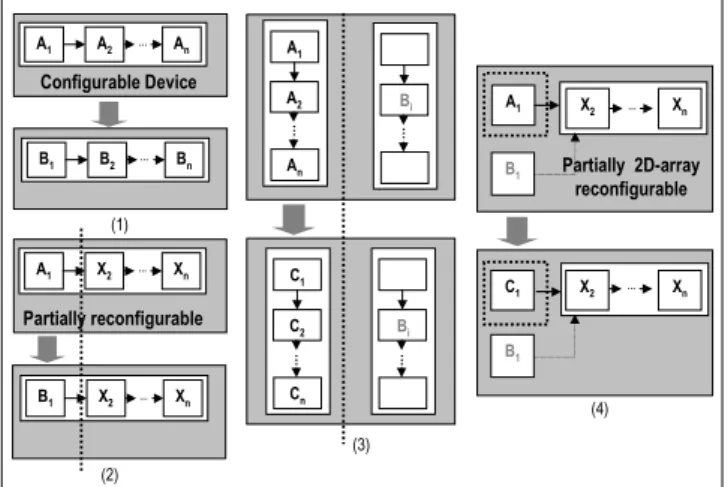
A thorough analysis of these reconfiguration approaches is presented hereafter and enables to propose different reconfiguration scheme (Figure 1) for a FPGA viewed as a hardware accelerator.
Full reconfiguration: The scenario illustrated in Figure 1.1 represents a full reconfiguration of the FPGA in order to reconfigure totally the application. In that case the FPGA that was executing application A is reconfigured in order to support application B.
Partial reconfiguration: The second example (Figure 1.2) corresponds to a partial reconfiguration of the FPGA for a partial reconfiguration of the application. This second type of implementation implies a precise analysis of the different applications to be mapped on the same FPGA in order to find the common components Xi which stay fixed and the components Ai and Bi that are reconfigured.
A drawback of both previous approaches is that the FPGA stops its execution while the reconfiguration is performed (it results on a timing overhead). Another solution is to implement both applications on the FPGA before switching from one to another as explained below. Two step reconfiguration: These two scenarios (Figure 1.3 and 1.4) describe a reconfiguration mechanism that is
Figure 1. Reconfiguration scenarios on FPGAs
A1 X2 … Xn Partially reconfigurable B1 X2 … Xn (2) A1 A2 … An Configurable Device B1 B2 … Bn (1) Partially 2D-array reconfigurable A1 X2 … Xn B1 C1 X2 … Xn B1 (4) (3) C1 C2 Cn … … A1 A2 An … … Bi Bi
performed in a two step approach. The first step leads to switch between two already implemented applications on the FPGA. For example in Figure 1.3 there is first a switch between application A and B. As the switch between both applications is very fast it enables to perform dynamic reconfiguration without considering the reconfiguration time overhead. The second step then manages the reconfiguration of the unused application. For example in Figure 1.3 the scenario is the following. First there is a switch between application A and B, then while the FPGA executes application B, application C is configured (partial reconfiguration of the FPGA) instead of application A that is now unused. When application B will be done we can imagine a switch with application C and then to reconfigure partially the FPGA to replace application B by a new one. Note that the scenario shown in Figure 1.3 is a partial device reconfiguration for a full application reconfiguration and scenario in Figure 1.4 is a partial application reconfiguration by a partial device reconfiguration.
Reconfiguration time: The main difference between these reconfiguration approaches is related to the reconfiguration time, which depends on the size of the logic to be reconfigured. In the two step reconfiguration approach as it is just a switch from one application to another the reconfiguration time can be considered to take only one clock cycle, but the drawback of that approach is that the FPGA must be larger which can be prohibitive for embedded systems.
Configuration memory: Concerning the configuration memory, the last reconfiguration scheme (Figure 1.4) requires that the FPGA supports partially matrix reconfiguration i.e., the FPGA must have 2D-array configuration memory (for example as available with Atmel component [11]). Other scenarios require 1D-array configuration memory (for example by column as available with Xilinx component [12]). 2D-array reconfigurable FPGAs are more efficient since the logic to be reconfigured is optimised. However components proposed by vendors using this technology does not offer today very high level of integration which limits their utilisation.
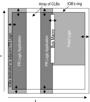
Communication links: Scenarios in Figure 1.2 and 1.4 require an interconnection (communication link) between the reconfigured parts and the fixed one. This point is particularly sensible since the interconnection must ensure at the logic level the data transmission continuity when different designs are re-mapped, re-placed and re-routed on the FPGA. Several solutions exist to overcome this problem and they will be described in further details in section 5. Figure 2 shows an example of implementation that results of a combination between the two different scenarios 1.2 and 1.3 on the Virtex [13]. This example illustrates communication links (Bus Macro). It presents also the problem of interfacing since I/O ports immediately above the top edge and below the bottom edge of a reconfigurable module are dedicated to this module which limits the availability of I/O ports to a single module.
Reconfiguration controller: Finally, two cases must be considered to perform reconfiguration on a FPGA. The reconfiguration controller can be external or internal (auto-configuration). In general the controller is
implemented in a processor (DSP or RISC) that is on the same board than the FPGA. However Virtex-II FPGA that embeds a processor can perform auto-configuration through the internal ICAP interface [14]. In that case just partial reconfiguration is possible. Whatever the solution considered, external or auto-configuration, it does not affect the reconfiguration time. The first solution will be discussed in details in section 3.
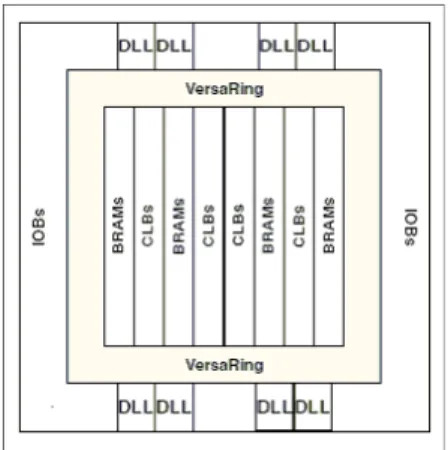
IV. SDR EXPERIMENTATION PLATFORM The development system that has been used to implement the modulation chain for multi-standards communication is based on a PCI carrier board composed of a TI C6201 DSP and a Xilinx Virtex 1000E FPGA (Figure 3) [15]. The DSP is running at 200 MHz and communicates to external components through six Com-Port working a 20 Mbytes/s. A 16 Mbytes SDRAM is linked to the DSP in order to store application code and data (it will also contains the bitstreams as explained in section 5). The Virtex 1000E (Figure 4) is island type architecture [16], which is composed of the Input Output Blocks
Control Data 50 MHz SDRAM Full Bitstream Partial Bitstream Partial Bitstream Data transfer Configuration transfer (bitstream) CP3 FPGA Virtex 1000 E CPLD CP4 CP2 CP0 DSP C62 Partial Module Fixed Module Bus Macro DSP Code
Figure 3. DSP/FPGA Sundance Platform Figure 2. Dynamic reconfiguration on FPGAsL
l IOB’s ring IOBs de di ca ted to ad ja cent PR Lo gi c PR Lo gi c Appl ic ati on PR Lo gi c Appl ic ati on Fi xe d Logi c Bu s Macro Array of CLBs
(IOBs), the Configurable Logic Blocks (CLBs) and the embedded RAM memories (BlockSelectRAM). The CLBs contain four logic slices. Each slice is composed of two four inputs LUTs, two registers and two fast carry chains. Four inputs LUT can perform any logic function of four inputs.
The DSP and the FPGA are connected through two Com-Ports, one dedicated to data transfers and another dedicated to bitstream transfers (i.e., for total and partial reconfigurations of the FPGA). In order to manage partial reconfiguration a CPLD is used to implement a configuration controller between the DSP and the FPGA. The configuration controller supports the SelectMap mode required to perform the configuration of the FPGA. Since DSP Com-Ports bandwidth is higher than SelectMap configuration speed, the FPGA configuration speed is managed at its maximum rate (i.e., 50 MHz). The DSP controls the FPGA reconfiguration through the CPLD with a master/slave-like communication protocol. This protocol is based on four commands, which permit the DSP to set or get the FPGA status, and to read or write the configuration data to/from the FPGA. These functions are included in the communication library in addition to the low-level Com-Port functions and the two higher level functions, which are called to configure the FPGA with a given full or partial bitstream. Part of the developed code for the communication library is presented hereafter.
Headers of the CPLD command functions that use the Com-Port dedicated to bitstream transfer
u32 CPLDGetStatus(Cp cp, u32 log)
void CPLDSetStatus (Cp cp, u32 data, u32 log) void CPLDWrite (Cp cp,u32 *bitstream_data, u32 bytecount)
//write one 32 bit word of bitstream data at index bytecode.
void FPGAReset(Cp cp)
High level function headers
void FPGAFullConfiguration(Cp cp, u32
*FullBitstream_array,u32 FullBitstream_Size) //call first FPGAReset() and after CPLDWrite() function
void FPGAPartialConfiguration(Cp cp, u32 * partialBitstream_array, u32
PartialBitstream_Size)
//just call CPLDWrite() in a loop of PartialBitstream_Size time.
It is important to know the bitstream structure to understand how to develop partially reconfigurable design. The Virtex configuration memory is organised as an array of bit. The elementary unit of configuration is the frame. It is a one-bit wide array and full height of the device. Frames are grouped together to form different types of columns (e.g., CLB, clock resources, BlockSelectRAM columns). For example, to configure one CLB, it is required to configure the 48 frames that compose the CLB configuration. These frames represent the entire CLB’s column plus 2 IOBs bordering on the top and the bottom of the CLB's column (Figure 5). Partial reconfiguration is only a column-based reconfiguration on the Virtex. In this study we have not focussed on the reconfiguration strategy (i.e., 2D or 1D reconfiguration) however some tools are now developed to directly handle the bitstream. They allow refining the reconfiguration bitstream just to the needed resources to be changed. Many of these tools are based on the Java class technology Jbits. A good overview of tools as JbitsDiff, PARBIT is done in [17].
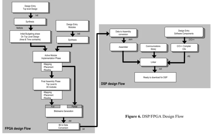
V. DESIGN FLOW
The design flow used to perform partial and dynamic reconfiguration on the DSP/FPGA platform is the following. First a component-based approach has been considered since as discussed for example by Kountouris and Moy in [6], it is generally admitted to be the right approach to realise Software Defined Radio terminal from the higher application layer to the baseband layer. In the case of digital baseband processing, components take the shape of processing blocks with some specific attributes described in details in the case study section. Furthermore component-based approach implies specific design rules. Independence and communication interfaces of processing blocks are essential points to consider during the design.
In our case the application is described with components written in MATLAB. Generic components can be designed for a common processing presents in the different algorithms (i.e., parameterisation). One reason among others to use MATLAB is due to the feasibility to choose all data widths of the application according to both the system level datapath specification and the accuracy expected on output data. After a validation step of the MATLAB specification, a manual hardware/software partitioning of the application is carried out. During that step a thorough analysis of the application is performed in
Figure 4. Virtex 1000E Architecture
order to exhibit the components that are candidates to dynamic reconfiguration.
The partitioning step leads to three inputs on the design methodology as shown in Figure 6. The DSP side input corresponds to the software components that are manually developed in C/C++ from the MATLAB specification and compile with Code Composer Studio for the TI C6201 DSP. The FPGA side inputs correspond to the hardware components that are described in VHDL (top-level design and each module as explained in the following). The FPGA design flow is based on the ISE 5.2 Xilinx tools with the XS T synthesis tool to generate a binary file called bitstream. Note that to configure the FPGA by the DSP each bitstream needs to be converted as an 8-bits data array that will be stored in the SRAM memory of the DSP.
A specific hardware design flow based on the Modular Design flow methodology [18] proposed by Xilinx is required to perform dynamic and partial reconfiguration. The top-level design entry corresponds to the structural view of the design. It instantiates the IOBs and the components required for the design. Each component is declared as a black box module with just its communication interfaces. The modules (or components) correspond to the other input of the Modular Design flow. Each Module is independent and has a unique body even if two types of module can be defined. The first type represents a single context that corresponds to one fixed part of the design. The other type represents multiple contexts. In this last case the context will change by partial reconfiguration. In other word, for a given top-level design, processing inside a multi-contexts module can be reconfigured dynamically without changing its connections inside the top-level design.
Modular Design implementation comprises the following phase [18], Initial Budgeting, Active Module
Implementation and Final Assembly. The first step, Initial Budgeting, consists in designing the floorplan of the target chip. Global logic is constrained in space and time and each module is sized end and positioned. Next in the Active Module Implementation phase, each context of each reconfigurable module and each fixed module are implemented according to the constraints defined on the top-level design. After this step, modules are placed and routed. In the Final Assembly phase, these placed and routed modules are merged in the top-level design where the global logic and IOBs are also placed and routed. A minimum of one full design implementation is required for the initial load on the FPGA before any partial reconfiguration.
The Virtex configuration memory described in section 3 imposes the following specific properties on each reconfigurable module [18]:
- The reconfigurable module height is always the full height of the device.
- IOBs immediately above the top edge and below the bottom edge of a reconfigurable module are part of the specific reconfigurable module's resources.
- Clocking logic (BUFGMUX, CLKIOBs) is always separate from the reconfigurable module. Clocks have separate bitstream frames.
- A reconfigurable module’s boundary cannot be changed. The position and region occupied by any single reconfigurable module is always fixed. The communication interface between a fixed module and a reconfigurable module is a complex issue. Reconfigurable modules communicate with other modules, both fixed and reconfigurable, by using a special bus called Bus Macro. A Bus Macro provides an inline four bits inter-core communication interface. Bus Macro is a pre-placed and pre-routed design, instantiable as a
Figure 6. DSP/FPGA Design Flow
DSP design Flow .asm Data to Assembly conversion Communications library Assembler Design Entry Software Components C/C++ Compiler C6x Linker .obj .C/C++ .out Ready to download for DSP Initial Budgeting phase
On Top Level Design (Area & Time contraints)
Design Entry Top level Design
Design Entry Modules Active Module Implementation Phase •Mapping •Placement •Routing Final Assembly Phase
Top Level & All modules •Mapping •Placement •Routing Bitstreams Generation Full Partial Synthesis Synthesis .hdl .hdl Netlists Bit to Data Conversion .dat .bit
black box in a design entry. The communication is done through tri-state buffers.
Once the bitstreams are generated they are converted to an assembly code in order to be merged with the software assembly code. The link step enables to gather the communication library routines, the program code and the bitstreams. Then the whole code is downloaded on the DSP memory and the application can be run. Each time a reconfiguration of the FPGA must be performed, the corresponding bitstream is downloaded from the DSP memory code into the reconfiguration memory of the FPGA.
VI. CASE STUDY
The initial objective of this study was to perform GSM to EDGE reconfiguration, which requires service continuity. In that case a reconfiguration from a Gaussian filter with MSK mapping (GSM) to Gaussian filter with 8PSK (EDGE) should have been performed. Right now as presented in the following we have demonstrated the concept of partial dynamic reconfiguration only from a Nyquist filter with QPSK mapping to Nyquist filter with 8PSK. That is the reason why 270 kHz has been considered for the symbol frequency. The use of 1.08 MHz enables to perform a digital IF carrier frequency, which corresponds to a classical Software Defined Radio
DFE.
The hardware/software partitioning of the modulation chains (Figure 7) that have been considered for this study (QPSK to 8PSK) leads to the following decomposition. Software components, which correspond to source coding simulation, DSP/FPGA data transfers and FPGA configuration transfers, are mapped to the DSP. The hardware components, which are bits to symbol coding (mapping), oversampling, filtering and IF transposition, are implemented in the FPGA. Bits to symbol coding component has been selected for partial dynamic reconfiguration since other components are common in both modulation chains.
Bits to symbol coding component carries out the serial to parallel bits transformation and the I/Q complex symbol mapping. Data bit rate for 8PSK is done at the frequency fb and for QPSK at 2/3fb to provide the same symbol frequency.
To design a unique interface for the bit to symbol coding component, an eight quantification bits width fixed communication interface is declared per channel. So the communication interface of this component instantiates 4 Bus Macro (two for each channel). During partial reconfiguration switching from QPSK to 8PSK leads to a reconfiguration of the logic resources (bit to symbol coding component) and the clock resources (using DLL) but communication interface remains unchanged (Bus
Figure 7. Partial dynamic reconfiguration scenario on a DSP/FPGA platform
Control Data 50 MHz SDRAM Full Bitstream Partial Bitstream 8PSK Partial Bitstream QPSK
Oversampling Filtering IF Transposition 8PSK/QPSK modulation chain
8PSK mapping QPSK mapping 1.08 MHz 1.08 MHz 270 KHz 810 KHz 540 KHz Data transfer Configuration transfer (bitstream) CP3 FPGA Virtex 1000 E CPLD CP4 CP2 CP0 DSP C62 Partial
Module ModuleFixed
Bus Macro Bits to symbol coding Reconfiguration Bits to symbol coding Source coding simulation
DSP/FPGA Sundance Platform
Macro). The fixed components on the FPGAs are the oversampling, the filtering and the IF transposition. Note that each of these components is implemented for both I and Q parts.
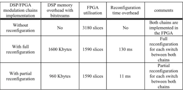
Table 3. QPSK/8PSK implementation scenarios DSP/FPGA modulation chains implementation DSP memory overhead with bitstreams FPGA
utilisation Reconfigurationtime overhead comments
Without
reconfiguration No 3180 slices No
Both chains are implemented in the FPGA With full
reconfiguration 1600 Kbytes 1590 slices 130 ms
Full reconfiguration for each switch between both
chains With partial
reconfiguration 960 Kbytes 1590 slices 11 ms
Partial reconfiguration for each switch between both
chains Several scenarios can be considered in order to compare partial reconfiguration with other solutions. Table 3 presents main characteristics of three scenarios. The first one does not implement reconfiguration, both chains are implemented in the FPGA. The second one uses dynamic reconfiguration but does not take benefit of partial reconfiguration (i.e., only full reconfiguration is performed). Finally, the last one uses dynamic and partial reconfiguration. For each solution, the DSP memory overhead due to the bitstreams and the reconfiguration instructions, the FPGA utilisation and the reconfiguration time overhead are highlighted. Between the solutions using or not the reconfiguration there is 50% reduction of the slices utilisation. This is normal in our case since with reconfiguration a single chain is implemented at any time on the FPGA.
The DSP memory overhead due to bitstreams is an important issue for embedded systems. The use of partial reconfiguration leads to almost 50% reduction of the memory overhead. In the case of partial reconfiguration the DSP memory overhead is composed of one full bitstream and both partial bitstreams (bit to symbol coding respectively for the QPSK and the 8PSK modulations) to be compare with two full bitstreams in the case of full reconfiguration.
Considering reconfiguration time overhead, partial reconfiguration leads to 90% reduction of the configuration time which is very important in order to guaranty services continuity. In the full reconfiguration scenario a full bitstream must be loaded on the FPGA for each reconfiguration. In the case of partial reconfiguration, the first bitstream must be a full bitstream and then only partial bitstreams are loaded. Hence for an execution schedule doing QPSK and then 8PSK modulations the benefit is almost 50% for the reconfiguration time. This benefit increases each time there is a new switching between both modulation chains. When possible partial dynamic reconfiguration presents an interesting solution since it enables an important FPGA utilisation reduction while leading to limited DSP memory and reconfiguration time overheads.
However, several design constraints are related to partial reconfiguration, like internal communication (Bus Macro) and external communication (IOBs). I/O ports availability for fixed design components depends on the place of the
reconfigurable module since IOBs adjacent to partially reconfigurable module are dedicated to it (Figure 2). Furthermore, number of I/O ports is proportional to the perimeter of the device while logic resources are proportional to the area of device in relation to the size and the package technology of the device. More the logic array increases more I/O resources represent a critical resource in this type of device as highlighted by the following equation:
IO
N ALR =α⋅
eq.1.
A
LR Logic Resource (Area) VS. ION Number of I/O (Perimeter)
A solution consists of using another type of package like a BGA one, which allows connecting I/Os anywhere on the die. The design of the QPSK/8PSK application has been confronted to the I/O ports difficulty since two Com-Ports of 32 bits width are required (one for data transfer between the DSP and the FPGA and the other for the two 16 bits width channel outputs).
Another important issue is the reconfiguration time, which is directly proportional to the size of the bitstream to be downloaded on the FPGA. In our case, during the floorplanning ten CLB columns have been reserved for the reconfigurable mapping module (bit to symbol coding) since it is not a complex module. On the Virtex 1000E the height of a column is 96 CLBs, which leads to a reconfiguration time around 11 ms. A column is reconfigured when just one CLB of the column is used. In our case the whole 10 columns will be reconfigured even if the whole CLBs 96×10 are not used. In order to evaluate the reconfiguration time overhead, estimation based on the CLBs reconfiguration can be carried out. One frame (on a Virtex 1000E) is composed of 1024 bits. One CLB column contains 48 frames, hence 48×1024 bits (around 60Kbits). After the floorplanning step the designer knows how many columns have been allocated to its partial reconfigurable module. For a 10 column design (i.e., case for the bit to symbol coding) the partial bitstream estimated size is equal to 10×60Kbits (600Kbits) thus 600/8=74Kbytes (to be stored in the DSP SRAM). The reconfiguration time computation can be performed as follows: time for reconfiguration = 74Kbytes/50Mhz = ~12 ms. 50Mhz corresponds to the configuration speed constrained by the FPGA.
Nevertheless the reconfiguration time given here is an upper limit and not the minimal time since all the CLBs contained in a column are reconfigured even if only one change. To optimise the reconfiguration time designer needs to use bitstream manipulation tools, to build a smaller bitstream and “emulate a 2D-array of reconfiguration”. A good overview of such tools is done in [17].
The last important limitation is related to the definition of a flexible and easy to use communication interface between reconfigurable module. In our case we have used classical Bus Macro, which is quite restrictive. To overcome this limitation several solutions are now proposed. For example, the Core Unifier proposed by [17] provides in addition to an interface a controller. The flexible Module Wrapper from Patterson [19] uses a column of CLBs at the left and the right of a module as a
configurable interface. The Gasket Interface [20] of the FPX system represents another possibility. All of these communication interfaces presents a higher flexibility than Bus Macro and can leverage the dynamic partial reconfiguration.
VII. CONCLUSION
We have presented the implementation of modulation chains for multi-standards communication in a context of Software Defined Radio. The contribution of this work is to prove the feasibility of dynamic and partial reconfiguration on a heterogeneous platform composed of one DSP and one FPGA. To perform this implementation we have focussed on the application, the platform and the design flow, which is an essential issue in order to make available the use of such approach. The benefits are important since dynamic partial reconfiguration increases the flexibility of hardware platform, which is mandatory for a Software Defined Radio approach. Use of FPGA permits to introduce this flexibility into typical functions of the Digital Front End of Software Defined Radio terminals.
There are still some limitations, we have tried to highlight them as internal communication through Bus Macro and bitstream manipulation. Xilinx Virtex II FPGAs and emerging tools for bitstream manipulation offer new possibilities to further increase the efficiency of dynamic and partial reconfiguration. Software Defined Radio paradigm is still an open topic concerning the execution platform however the implementation of modulation chains for multi-standards communication proves the availability of new technology to support such paradigm. The combination of a component approach with parametrisation studies for the application side and the possibilities of new design like run-time adaptive core for the reconfigurable architecture side will provide a way to propose new architectural paradigm for an optimised Software Defined Radio execution platform.
VIII. REFERENCES
[1] R.J. Lackey, D.W. Upmal, Speakeasy: The Military Software Radio, IEEE Communications Magazine, May 95, pp.56-61.
[2] J. Mitola, The software Radio architecture, IEEE Communication Magazine, May 1995, pp. 26-38. [3] A. Polydoros, J. Rautio, G. Razzano, H. Bogucka, D.
Ragazzi, P. I. Dallas, A. Mämmelä, M. Benedix, M. Lobeira, L. Agarossi, WIND-FLEX: Developing a Novel Testbed for Exploring Flexible Radio Concepts in an indoor Environment, IEEE Comms. Mag, vol.41, no 7, july 2003.
[4] H. Harada, Y. Kamio, M. Fujise, Multimode Software Radio System by Parameter Controlled and Telecommunication Component Block Embedded Digital Signal Processing Hardware, IEICE Trans. Commun., vol.E83-B, no.6 june 2000.
[5] J. Palicot, C. Roland, FFT: a Basic Function for a Reconfigurable Receiver, ICT’03, Feb. 2003.
[6] A. A. Kountouris, C. Moy, Reconfiguration in software radio systems, 2nd Karlsruhe Workshop on SR. 2003.
[7] R. Srikanteswara, R. Chembil Palat, J. H. Reed, and P. Athanas, An overview of configurable computing machines for Software Radio handsets, IEEE communications magazine, July 2003.
[8] R. Hartenstein, A decade of reconfigurable computing: a visionary retrospective, DATE’01 [9] M. Cummings, S. Haruyama, FPGA in the Software
Radio, IEEE Comms. Mag., Feb. 1999.
[10] K. Danne, C. Bobda, H. Kalte, Increasing Efficiency by Partial Hardware reconfiguration, Case Study of a Multi-Controller System, ERSA, 2003
[11] Atmel AT40K FPGA Data Sheet, www.atmel.com [12] Xilinx, Virtex Series Configuration Architecture
User Guide, Application Note 151, 2003.
[13] Xilinx Virtex-E FPGA Data Sheet DS022, www.xilinx.com, July 2002.
[14] B. Blodget, P. J. Roxby, E. Keller, S. McMillan, P. Sundarajan, A self-reconfiguring Platform, FPL 2003.
[15] Sundance, SMT358 User Manuel, version 2.5 and SMT335/SMT375 User Manuel, version 3.2. [16] K. Compton, S. Hauck, Configurable Computing, A
Survey of System and Software, Northwestern University USA, technical report, 1999.
[17] D. Mesquita, F. Moraes, J. Palma, L. Möller, N. Calazans, Remote and Partial Reconfiguration of FPGAs: tools and trends, IPDPS'03, 10th RAW, Nice, April 22 - 26, 2003.
[18] D. Lim, M. Peattie, Two Flows for Partial Reconfiguration: Module Based or Small Bit Manipulations, Appl. note 290, Xilinx, 2002. [19] C. D. Patterson, A Dynamic Module Server for
Embedded Platform FPGAs, ERSA, 2003.
[20] E. L. Horta, J. W. Lockwood, D. Parlour, Dynamic Hardware Plugins in an FPGA with Partial Runtime Reconfiguration, DAC, 2002.