HAL Id: hal-01428657
https://hal.archives-ouvertes.fr/hal-01428657
Submitted on 21 Jun 2018HAL is a multi-disciplinary open access archive for the deposit and dissemination of sci-entific research documents, whether they are pub-lished or not. The documents may come from teaching and research institutions in France or abroad, or from public or private research centers.
L’archive ouverte pluridisciplinaire HAL, est destinée au dépôt et à la diffusion de documents scientifiques de niveau recherche, publiés ou non, émanant des établissements d’enseignement et de recherche français ou étrangers, des laboratoires publics ou privés.
polymer-based optical phase modulator using 1D and
2D photonic crystal structures
Kevin Receveur, Kai Wei, Massinissa Hadjloum, Mohammed El Gibari,
Alfredo de Rossi, Hong Wu Li, Afshin S. Daryoush
To cite this version:
Kevin Receveur, Kai Wei, Massinissa Hadjloum, Mohammed El Gibari, Alfredo de Rossi, et al.. Sensitivity improvement of broadband electro-optic polymer-based optical phase modulator using 1D and 2D photonic crystal structures. Chinese Optics Letters, Optical Society of America (imprimé) / OSA publishing (en ligne), 2017, 15 (1), pp.010003. �10.3788/COL201715.010003�. �hal-01428657�
Sensitivity improvement of broadband electro-optic
polymer-based optical phase modulator using
1D and 2D photonic crystal structures
K. Receveur1 , K. Wei1 , M. Hadjloum2 , M. El Gibari2 , A. De Rossi3 , H. W. Li2 , and A. S. Daryoush1, * 1
Department of ECE, Drexel University, Philadelphia, PA 19104 USA
2
IETR, Université Bretagne Loire, University of Nantes, 44322 Nantes, France
3
Thales Research and Technology France, 91767 Palaiseau, France *Corresponding author: adaryoush@coe.drexel.edu
Received October 15, 2016; accepted December 6, 2016; posted online January 6, 2017
This Letter introduces the design and simulation of a microstrip-line-based electro-optic (EO) polymer optical phase modulator (PM) that is further enhanced by the addition of photonic crystal (PhC) structures that are in close proximity to the optical core. The slow-wave PhC structure is designed for two different material configu-rations and placed in the modulator as a superstrate to the optical core; simulation results are depicted for both 1D and 2D PhC structures. The PM characteristics are modeled using a combination of the finite element method and the optical beam propagation method in both the RF and optical domains, respectively. The phase-shift simulation results show a factor of 1.7 increase in an effective EO coefficient (120 pm/V) while maintaining a broadband bandwidth of 40 GHz.
OCIS codes: 230.0230, 250.0250, 130.0130, 130.0250, 130.4110, 130.5296, 130.5460, 160.2100, 160.4236.
doi: 10.3788/COL201715.010003.
The combination of silicon photonics and electro-optic (EO) polymers in optical devices enables the fabrication of high-level photonic device integration[1] using CMOS
compatible nanofabrication technology[2]. The use of EO
polymers allows for a large EO coefficient (r33), very low
dispersion, a fast response time (<1 ps), and simple fabri-cation[3,4]. Compared to the limitations of traditional
inor-ganic crystal modulators in terms of the EO coefficient (r33∼ 30 pm∕V), the use of a synthesized EO polymer
al-lows a higher EO coefficient (r33¼ 138 pm∕V at 1550 nm)
due to the progress of chromophore synthesis and the high efficiency of poling; this improvement allows for a better modulation efficiency[5]
and extremely high modulation speeds of over 150 GHz[6,7]
. These benefits are crucial in cre-ating an efficient optical modulator design, either in terms of a realized phase or intensity[8–10]modulations. The high sensitivity of phase and intensity modulators has been cru-cial in various applications, such as opto-electronic oscilla-tors[11]
and optical deflectors in an all-optical analog to digital converter[12]
.
Both the device length and driving voltage can be further reduced by introducing advanced modulator designs using a photonic crystal (PhC)-based slow-wave material. PhC materials exhibit slow-lightwave effects, which can be used to effectively increase the sensitivity of the EO index modu-lation[13]. The ability to slow down the light passing through
a modulator allows for a reduced group velocity, as the lightwave is traveling through the material. The slow light-wave in PhC materials enhances the in-device phase shifts and creates an even more efficient phase modulation[14]
. Modulators using PhC materials have been explored using a combination of ceramic-air materials[15]
as well as
ceramic-EO polymer PhC structures[16]
. In recent years, studies have focused on EO polymers in combination with silicon 1D and 2D PhC waveguides[17,18], which greatly
im-prove the effective EO coefficient of the modulator design. The majority of recent modulator designs use a lateral modulator design; however, a vertical design using PhC is yet to be explored. This design with PhC requires more manufacturing sensitivity and also introduces challenge to fabricate air gaps inside a PhC material.
This Letter introduces the performance improvement of the EO polymer-based vertical phase modulator design us-ing integrated 1D and 2D PhC structures to a microstrip transmission line. The addition of PhC will enhance the effective EO coefficient to improve the optical phase modulation sensitivity by slow-wave PhC structures. The addition of the PhC material as either a superstrate above the optical core or a substrate below the optical core produces an improved modulator figure of merit for a broad bandwidth of operation up to 40 GHz.
The vertical modulator topology, shown in Fig.1, is in-duced by placing two copper electrodes on the top and bottom of a substrate material. Between the two electro-des, an optical core made out of an EO polymer (CPO-1) using polymethyl methacrylate (PMMI) as a host material (n¼ 1.63, εr ¼ 3.15, tan δ < 10−2) is placed surrounded
by the cladding material, Norland Optical Adhesive 65, or NOA65 (n¼ 1.51, εr ¼ 3.2, tan δ ¼ 2.2 × 10⁻²), an
optical adhesive cured by UV light. The optical core was chosen to be a¼ 1.6 μm and b ¼ 1.6 μm, confining the wave to a single TEM-like mode beyond 1400 nm. The thickness of the electrodes was chosen to be 2 μm. The height of the NOA65 material and the width of the
top Cu electrode are determined to match the microstrip RF transmission line to a characteristic impedance (Z0)
of 50 Ω, reducing RF dispersion characteristics and mismatch-induced losses over the phase modulator length, L, of 1 cm.
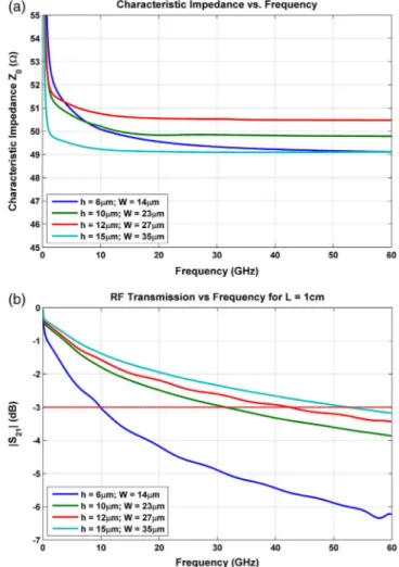
The RF characteristics of the modulator, shown in Fig. 2, were simulated using the finite element method (FEM) with a commercial product, HFSS[19]
. The sub-strate height, h, was optimized to 12μm with an electrode width of w¼ 27 μm. This attained a characteristic imped-ance of 50.8Ω with a 3-dB RF attenuation bandwidth of 42.5 GHz for a 1 cm long phase modulator design. Optical wave simulations were performed using the beam propa-gation method (BPM) through use of the OptiBPM commercial software[20].
For each simulation, the EO coefficient of the polymer was selected to be 70 pm/V. The modulator figure of merit, Vπ× L, was determined to be 6.5 V·cm with an optical loss of 1.8 dB/cm. The effective r33 of the modulator
was then determined to be 68.7 pm/V from[8]
r33eff ¼ λ 0h
2n3optΓVπL
: (1)
Designs of the 1D and 2D PhC structures are conducted using the plane wave expansion (PWE) method using the FEM for verification in 3D in the HFSS. Two topologies of PhC were selected: the first one uses a varying dielectric of a PMMI/EO polymer and Si3N4(n¼ 2.46), and the
sec-ond one uses a combination of a PMMI/EO polymer and air gaps within the material in order to compare two slow-wave structure models. Si3N4was selected due to its close
refractive index value to the one for the core material. The latter topology is very popular with lateral phase modu-lators but is impractical for vertical topologies. The first
topology is reported here, and it is considered for both superstrate and substrate formats.
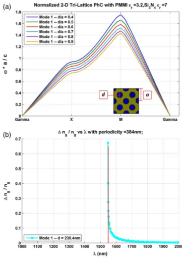
The 1D structure material design consists of a base material of PMMI/EO polymer, with a substrate width d, of either air gaps or Si3N4. The total periodicity of the
material is determined by a. For the PMMI∕Si3N4
combi-nation [Fig.3(a)], the periodicity was selected as 318 nm with an Si3N4 layer width of 192 nm. The region of
oper-ation was chosen as very close to the band edge of the material, utilizing the slow light produced by the periodic PhC material. The slowness characteristics of the material are shown in Fig.3(b)through the percent change in the group index of the material. This change in the group index indicates a slowdown in the group velocity of the wave. This change in group index for the PMMI∕Si3N4material
at 1550 nm was determined to be 28% for the above periodicity.
The 2D structure material design consists of a base material of a PMMI/EO polymer surrounding periodic cylinders made out of an Si3N4 material. The design
parameters consist of the cylinder radius, d, and the perio-dicity between holes, a. For the PMMI∕Si3N4
combina-tion [Fig. 4(a)], the periodicity was selected as 384 nm
Fig. 1. Conceptual overview of a baseline EO polymer-based traveling-wave optical phase modulator design; (a) X–Y cross section, and (b) X–Z cross section.
Fig. 2. Performance of 50 Ω microstrip-line traveling-wave structure versus the frequency for various substrate heights: (a) dispersion of characteristic impedance, and (b) RF insertion loss over 1 cm length.
with an Si3N4hole diameter of 230 nm. The slowness
char-acteristics of the material are shown in Fig.4(b)through the percent change in the group index of the material. Sim-ilarly for the PMMI∕Si3N4 1D structure, the increased
group index results in the reduced group velocity of the lightwave. A 51% change in the group index was deter-mined for a periodic PMMI∕Si3N4 material at 1550 nm.
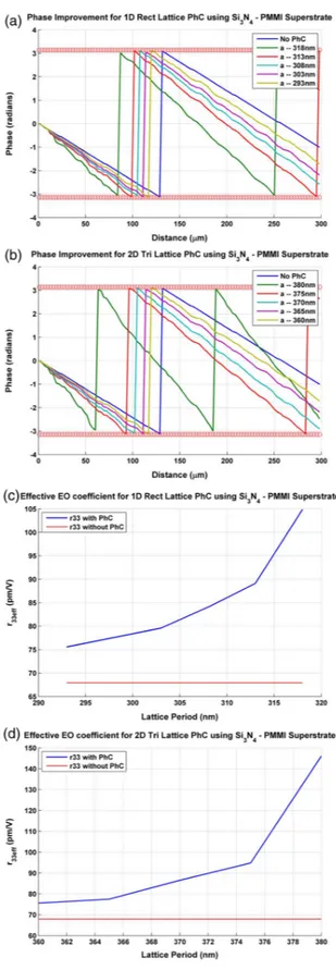
To incorporate a slow-wave effect inside the baseline modulator, the PhC structures were placed as either a superstrate [Fig. 5(a)] or a substrate design. Similar to Fig. 5(a), the PhC material interacts with optical waves in the optical core by placing it below instead of above. A buffer layer of NOA65 is placed above or below the core to control the interactions between the optical core and the 1D or 2D PhC while mitigating optical losses. The slow-wave structure was simulated using a combina-tion of FEM and BPM modeling to determine the optical characteristics as a wave was injected into the modulator. The zoomed-in details of the optimized design using 1D and 2D PhC dimensions are shown in Fig.5(b)and5(c),
respectively, where the optimum width and thickness of 1.6μm and 500 nm for the PhC were determined by the tradeoff between the figure of merit (Vπ× L) and the op-tical loss within the core through consecutive modeling. An optimum cladding/buffer layer was also determined in a similar modeling manner to be 500 nm. The original modu-lator length was shortened to 300μm in order to have a higher resolution for each BPM node and for computa-tional efficiency. An equivalent driving voltage of 400 V for 300μm (rather than 12 V for 1 cm) was applied to the modulator electrodes to observe the phase change within this short device. The Vπ value was determined by the amount of voltage it takes to shift the phase of the modu-lator byπ rad. This value is then multiplied by the modu-lator length, L, to find the phase modumodu-lator figure of merit. It is shown in Fig.6(a)and6(b)that the phase change increases as the periodicity approaches the theoretical value. Employing this change in periodicity, the Vπ value can be optimized. Using the 1D PMMI∕Si3N4superstrate
case, the modulator figure of merit was determined to be 3.36 V·cm at a periodicity a of 318 nm, while using the
Fig. 3. Slow-wave modeling results for PMMI∕Si3N4 PhC
material: (a) Normalized dispersion diagram of 1D PhC using varying dielectric of PMMI∕Si3N4material with a as the PhC
periodicity and d as the Si3N4layer thickness. (b) Change in group index relative to the operating wavelength for a¼ 318 nm and d¼ 192 nm. The red line represents the performance at λ ¼ 1550 nm.
Fig. 4. Slow-wave modeling results for PMMI∕Si3N4 PhC
material: (a) Normalized dispersion diagram of 2D PhC using varying dielectric of PMMI∕Si3N4material with a as the PhC
periodicity and d as the Si3N4hole diameter. (b) Change in group index relative to the operating wavelength for a¼ 384 nm and d¼ 230 nm. The red line represents the performance at λ ¼ 1550 nm.
2D PMMI∕Si3N4 superstrate case, the figure of merit
(Vπ× L) was simulated to be 2.41 V·cm at a periodicity a of 360 nm.
The effective EO coefficient r33eff is then calculated
using Eq. (1), whereλ ¼ 1550 nm, h ¼ 12 μm, nopt¼ 1.6,
L¼ 300 μm, and Γ ¼ 0.9. In Fig. 6(c), the effective EO coefficient for the PMMI∕Si3N4case was then determined
to be 104.9 pm/V, whereas in Fig.6(d), the EO coefficient for the 2D PMMI∕Si3N4 case was determined to be
146.1 pm/V, which improves the modulator EO coeffi-cient by about a factor of 1.5 and 2.1, respectively, com-pared to the baseline traveling-wave design without PhC. The superstrate results were evaluated in a similar man-ner. By comparing the velocity mismatch between the group index of the optical and RF waves, the bandwidth of each modulator design is limited by the RF attenuation to 40 GHz, while an improved figure of merit is observed for the modulator. Adding a PhC in the superstrate or substrate, however, warrants unwanted losses from the PhC structure in addition to manufacturing challenges. For the superstrate case, the total optical losses through the 1D and 2D PMMI∕Si3N4PhC designs were simulated
as 4.6 and 4.0 dB/cm, respectively, compared to
Fig. 5. Improved phase modulator design and results using a 1D or 2D PhC superstrate as a slow wave: (a) cross-sectional view of a phase modulator, (b) zoomed-in view of 1D PhC layer as a superstrate to the optical core with PhC width¼ 1.6 μm, PhC thickness¼ 500 nm, and a buffer layer of 500 nm, and (c) zoomed-in view of 2D PhC layer as a superstrate to the op-tical core with PhC width¼ 1.6 μm, PhC thickness ¼ 500 nm, and a buffer layer of 500 nm.
Fig. 6. (a) The wrapped-around achieved phase variation as a function of the phase modulator with and without 1D PhC slow-wave structures of PMMI∕Si3N4, (b) the wrapped-around
achieved phase variation as a function of the phase modulator with and without 2D PhC slow-wave structures of PMMI∕Si3N4,
(c) effective EO coefficient based on the optimum periodicity a, 318 nm, of the 1D PMMI∕Si3N4 PhC lattice, and (d) effective
EO coefficient based on the optimum periodicity a, 360 nm, of the 2D PMMI∕Si3N4PhC lattice.
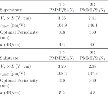
1.8 dB/cm in the original structure. Results for all consid-ered topologies are summarized in Table1.
Compared to the characteristics of the baseline modulator design with Vπ× L¼ 6.5 V·cm (i.e., r33 ¼
68.7 pm∕V), each of the designs offered at least 60% im-provement in the figure of merit Vπ× L, which effectively increased by 60% the resulting“effective” EO coefficient. In conclusion, this Letter demonstrates realistic full-wave modeling of an EO polymer-based vertical realiza-tion of an optical phase modulator design, where its phase modulation sensitivity is enhanced by 1D or 2D PhC structures. Enhancement of the phase modulator response is due to the slow-wave effect in 1D and 2D PhC struc-tures. This enhancement is quantified by comparison of the device figure of merit of Vπ× L¼ 3.26 V·cm for a PMMI∕Si3N4substrate to 6.5 V·cm for the baseline bulk
design; hence, improved EO is attained by nearly doubling the coefficient with an RF bandwidth of 40 GHz.
The superstrate and substrate designs evaluated offer an improvement over the baseline bulk phase modulator to different degrees of effective EO coefficient; however, the optical loss increases with the new structure. The 2D PMMI∕Si3N4 PhC combination offers a better
improve-ment in the figure of merit and relative optical loss charac-teristics with an optical wave confinement of the first mode to the PMMI/EO polymer portion of the PhC. Numerical calculations and performance simulations of 1D and 2D PhC using a PMMI/air combination are also performed but not reported here; even though it seems to be more ef-fective in its phase modulation efficiency, the PMMI∕Si3N4
results are more practical in terms of fabrication process, since there is no access to the modulators from the top in the vertical topologies when the placement of air gaps
cannot be realized, as compared to the lateral modulator designs. In addition, the fabrication of a PhC substrate layer allows for more variability during the microfabrica-tion process steps and should be avoided. A lateral design is also being considered to employ an efficient Mach– Zehnder intensity modulator, where an RF injection method and optical mode converter are required for various applications, such as opto-electronic oscillators[11,21].
References
1. J. Leuthold, C. Koos, W. Freude, L. Alloatti, R. Palmer, D. Korn, J. Pfeifle, M. Lauermann, R. Dinu, S. Wehrli, M. Jazbinsek, P. Günter, M. Waldow, T. Wahlbrink, J. Bolten, H. Kurz, M. Fournier, J. M. Fedeli, H. Yu, and W. Bogaerts, IEEE J. Sel. Top. Quantum Elec-tron. 19, 114 (2013).
2. R. Soref, IEEE J. Sel. Top. Quantum Electron. 12, 1678 (2006). 3. D. Chen, H. R. Fetterman, A. Chen, W. H. Steier, L. R. Dalton, W.
Wang, and Y. Shi, Appl. Phys. Lett. 70, 3335 (1997).
4. X. Lin, T. Ling, H. Subbaraman, X. Zhang, K. Byun, L. J. Guo, and R. T. Chen, Opt. Lett. 38, 1597 (2013).
5. Y. Enami, C. T. Derose, D. Mathine, C. Loychik, C. Greenlee, R. A. Norwood, T. D. Kim, J. Luo, Y. Tian, A. Y. Jen, and N. Peygham-barian, Nat. Photon. 1, 180 (2007).
6. B. Bortnik, Y. C. Hung, H. Tazawa, B. J. Seo, J. Luo, A. K. Y. Jen, W. H. Steier, and H. R. Fetterman, IEEE J. Sel. Top. Quantum Elec-tron. 13, 104 (2007).
7. M. Lee, H. E. Katz, C. Erben, D. M. Gill, P. Gopalan, J. D. Heber, and D. J. McGee, Science 298, 1401 (2002).
8. L. Thylen, U. Westergren, P. Holmström, R. Schatz, and P. Jänes, Opt. Fiber Telecommun. V., IP Kaminow 5, 183 (2008).
9. R. Palmer, S. Koeber, E. L. Delwin, M. Woessner, W. Heni, D. Korn, M. Lauermann, W. Bogaerts, L. Dalton, W. Freude, J. Leuthold, and C. Koos, J. Lightwave Technol. 32, 2726 (2014).
10. W. H. Steier, A. Chen, S. S. Lee, S. Garner, H. Zhang, V. Chuyanov, L. R. Dalton, F. Wang, A. S. Ren, C. Zhang, and G. Todorova, Chem. Phys. 245, 487 (1999).
11. T. Sun, L. Zhang, K. Receveur, A. K. Poddar, U. L. Rohde, and A. S. Daryoush, in IEEE MTT-S International Microwave Symposium (IMS 2015) (2015).
12. M. Hadjloum, M. El Gibari, H. Li, M. Halbwax, J. P. Vilcot, and A. S. Daryoush, in IEEE 2015 Microwave Photonics Meeting (MWP2015) (2015).
13. T. Baba, Nat. Photon. 2, 465 (2008).
14. H. C. Nguyen, S. Hashimoto, M. Shinkawa, and T. Baba, Opt. Ex-press 20, 22465 (2012).
15. Y. A. Vlasov, M. O'Boyle, H. F. Hamann, and S. J. McNab, Nature 438, 65 (2005).
16. J. M. Brosi, C. Koos, L. C. Andreani, M. Waldow, J. Leuthold, and W. Freude, Opt. Express 16, 4177 (2008).
17. S. Inoue and A. Otomo, Appl. Phys. Lett. 103, 171101 (2013). 18. X. Zhang, C. J. Chung, A. Hosseini, H. Subbaraman, J. Luo, A. Jen,
R. Neilson, C. Lee, and R. T. Chen, IEEE J. Lightwave Technol. 34, 2941 (2015).
19. Optiwave.s software OptiBPM, “Ansys HFSS,” Version 12.2:
http://ansys.com/, Capella Court, Ottawa (2016).
20. Ansoft’s software of HFSS from Ansys, Inc., “Optiwave OptiBPM,” Version 14.0:http://optiwave.com/, Ansys Drive, Canonsburg, PA (2016).
21. L. Zhang, A. K. Poddar, U. L. Rohde, and A. S. Daryoush, IEEE Photon. J. 6, 1 (2014).
Table 1. Performance Comparison of Various Phase Modulator Design Topologies Using Superstrate and Substrate 1D PhC Superstrate 1D PMMI∕Si3N4 2D PMMI∕Si3N4 Vπ× L (V·cm) 3.36 2.41 r33eff (pm/V) 104.9 146.1 Optimal Periodicity (nm) 318 360 α (dB/cm) 4.6 4.0 Substrate 1D PMMI∕Si3N4 2D PMMI∕Si3N4 Vπ× L (V·cm) 3.26 2.38 r33eff (pm/V) 108.4 147.8 Optimal Periodicity (nm) 318 360 α (dB/cm) 5.2 4.8