HAL Id: hal-00602889
https://hal.archives-ouvertes.fr/hal-00602889
Submitted on 23 Jun 2011HAL is a multi-disciplinary open access archive for the deposit and dissemination of sci-entific research documents, whether they are pub-lished or not. The documents may come from teaching and research institutions in France or abroad, or from public or private research centers.
L’archive ouverte pluridisciplinaire HAL, est destinée au dépôt et à la diffusion de documents scientifiques de niveau recherche, publiés ou non, émanant des établissements d’enseignement et de recherche français ou étrangers, des laboratoires publics ou privés.
High Efficiency White Luminescence of Alumina doped
ZnO
Alban A. Letailleur, Sergey Yu Grachev, Etienne Barthel, Elin Sondergard,
Komla Nomenyo, Christophe Couteau, Stefan Mc Murtry, Gilles Lerondel,
Emilie Charlet, Emmanuelle Peter
To cite this version:
Alban A. Letailleur, Sergey Yu Grachev, Etienne Barthel, Elin Sondergard, Komla Nomenyo, et al.. High Efficiency White Luminescence of Alumina doped ZnO. Journal of Luminescence, Elsevier, 2011, 131 (12), pp.2646-2651. �10.1016/j.jlumin.2011.06.044�. �hal-00602889�
High Efficiency White Luminescence of Alumina doped ZnO
Alban A. Letailleur,1,2,3,* Sergey Yu Grachev,1 Etienne Barthel,1 Elin Søndergård1, Komla Nomenyo,2 Christophe Couteau,2 Stefan Mc Murtry,2 Gilles Lérondel,2 Emilie Charlet,4 Emmanuelle Peter4
1
Surface du Verre et Interfaces, UMR 125 CNRS/Saint-Gobain, 39 quai Lucien Lefranc, BP
135, 93303 Aubervilliers Cedex, France
2
Laboratoire de Nanotechnologie et d’Instrumentation Optique, Institut Charles Delaunay,
CNRS UMR 6279, Université de Technologie de Troyes, 12 rue Marie Curie, BP 2060, 10010
Troyes Cedex, France
3
Laboratoire de Chimie de la Matière Condensée de Paris, UMR CNRS 7574, UPMC-
Université Paris VI, Collège de France, 11 place Marcelin Berthelot, 75231 Paris, France
4
Thin Films Division, Saint-Gobain Recherche, 39 quai Lucien Lefranc, BP 135, 93303
Aubervilliers Cedex, France
* alban.letailleur@saint-gobain.com, tel:+33 1 48 39 59 56, fax: + 33 1 48 39 55 62
Abstract
The application of Alumina-doped ZnO (AZO) films as luminescent material for large area lighting sources has been evaluated. Thin films were grown on quartz using magnetron sputtering and subsequently annealed under argon atmosphere in a rapid thermal annealing experiment. Below 550 °C, red-shift of the optical band gap and increase of the visible emission are observed in agreement with Al diffusion and formation of interstitial oxygen atoms. At temperatures higher than 800 °C, diffusion is activated and Ostwald ripening leads to the formation of larger grains and an increase of the crystalline phase. The photoluminescence (PL) intensity is enhanced, specifically in the UV range. As a result the emission spectrum of AZO thin films can be adjusted by the annealing conditions, with equal
contributions from the UV and orange parts of the PL spectrum resulting in an efficient white emission as quantified using the color space map of the Commission Internationale de l’Éclairage.
Keywords: Zinc oxide; doping; white luminescence; rapid annealing
1. Introduction
Zinc oxide (ZnO) is an abundant and non toxic oxide which has been widely used as catalyst, sun screen or for medical applications.1 A more recent interest focuses on the optoelectronic properties of ZnO. With a direct band gap of 3.37 eV and an exciton binding energy of 60 meV, ZnO is a promising candidate for room temperature ultraviolet optoelectronic devices, such as light emitting diodes.2
The luminescence of ZnO presents a wide variety of emission lines, with strong dependence to structural details. Photoluminescence (PL) spectra are usually separated in two contributions: a UV-peak around 380 nm and a visible contribution. Whereas the UV line is associated with the exciton recombination, the exact origin of the visible luminescence is still controversial.3 Defects inside the material act as strong recombination centers and emission bands are generated by donor-acceptor pair transitions. Those defects can be oxygen or zinc vacancies or interstitial atoms, or even pollutants.4
A large variety of n-dopants can be incorporated inside the ZnO to increase the range of applications from spintronics,5 ferroelectric layers,6 or transparent conductive oxide.7 Doping or co-doping the layer (with elements from the groups I, IIIb or V) modifies the energy levels and is also widely used to adjust the luminescence properties of ZnO thin films, by either shifting or broadening the several emission peak.8 Al doping leads particularly to a yellow luminescence,9 whereas Li doping is used to adjust the peak position and its intensity.10
Co-doping of these elements therefore leads to a broad-band yellow-white emission.11 Obtaining a white luminescence with Alumina-doped ZnO (AZO) is therefore a challenge.
There is an emergent need for large lighting sources. To obtain AZO thin films on large areas and achieve a precise control over the doping, solution-based processing (like the sol-gel method) is widely used.12,13 However, the large solvent content inside the material leads to porosity and reduces coating life-time. Along the physical method used for the AZO deposition, magnetron sputtering emerges as an easy way to coat surfaces at the window scale. The versatility of this method enables the deposition on various substrates such as sapphire,14 silicon,15 or glass.16
To improve the coating properties after deposition, samples are subsequently annealed. Control over the annealing atmosphere is of great importance to obtain the desired properties. Annealing in air or oxygen generally leads to a strong increase of the visible luminescence and a reduction of the UV peak.17,18 This can subsequently be recovered by annealing the sample under reducing atmosphere.19 Furthermore, annealing in vacuum or under nitrogen leads to a specific increase of the UV part of the spectrum.20
In applications, fast annealing is a requisite. In this work, we have probed the impact of Rapid Thermal Annealing on the luminescence of AZO thin films on quartz. The films were annealed during five minutes under argon atmosphere at temperatures up to 950 °C. The structural and optical properties of the obtained films were investigated. Impact on the luminescence was determined. In particular we show that white luminescence can be obtained in specific conditions.
2. Materials and Methods
The AZO films were grown on quartz substrates (synthetic quartz, Shin-Etsu, Japan) by RF magnetron sputtering from an AZO target (GfE Fremat, Germany). Quartz was chosen as
substrate because of its high transparency in the visible and UV ranges and for its chemical stability. The doping amount of Al2O3 in the AZO target ranged between 1 and 4 weight
percent.
Quartz wafers (10x10 cm²) were used as received and placed onto a 30x30 cm² glass plate into the sputtering chamber. The chamber was evacuated to 10-6 mbar. Argon was introduced through a mass flow controller and the working pressure was maintained to 8-10·10-3 mbar. The input power was kept at 2 000 W. The substrates are in translation under the AZO target and the growth rate is 30 nm.m-1.min-1.
The thickness of the films was 750 nm as measured with a surface profilometer (DEKTAK 3, USA) and Scanning Electron Microscopy (SEM, LEO DSM 982 Gemini).
The AZO samples were subsequently cut into pieces of 2x2 cm² and placed into the annealing oven. The chamber was flushed with argon during 10 min prior to annealing, and the gas flow (50 sccm) was maintained during annealing. The heating time was set to 10 s and the cooling rate was about 5 K.s-1. Samples were annealed at different temperatures Ta
(between 350 °C and 950 °C) for various times ta (between 15 s and 300 s).
X-Ray diffraction (XRD) film patterns were obtained with a PHILIPS PW1830 diffractometer (θ-2θ Bragg-Brentano geometry) operating with Cu Kα radiation (λ=1.5418 Å) and equipped with a graphite back monochromator.
Optical transmissions of the films were measured under normal incidence by a UV–VIS spectrophotometer between 350 and 800 nm. Photoluminescence (PL) spectra were collected at room temperature under normal incidence using a 50 cm focal length spectrometer with a 300 gr/mm grating, coupled to a Peltier-cooled CCD camera. Samples were excited at an incidence angle of 50 ° using a 325 nm He–Cd laser with an output power of 5 mW. The laser beam was focused to 100 µm with a 35 mm aspherical lens. The presented spectra were corrected by the spectral responses of the measurement set-up.
3. Results and discussion
3.1 Effect of annealing temperature on the structural properties
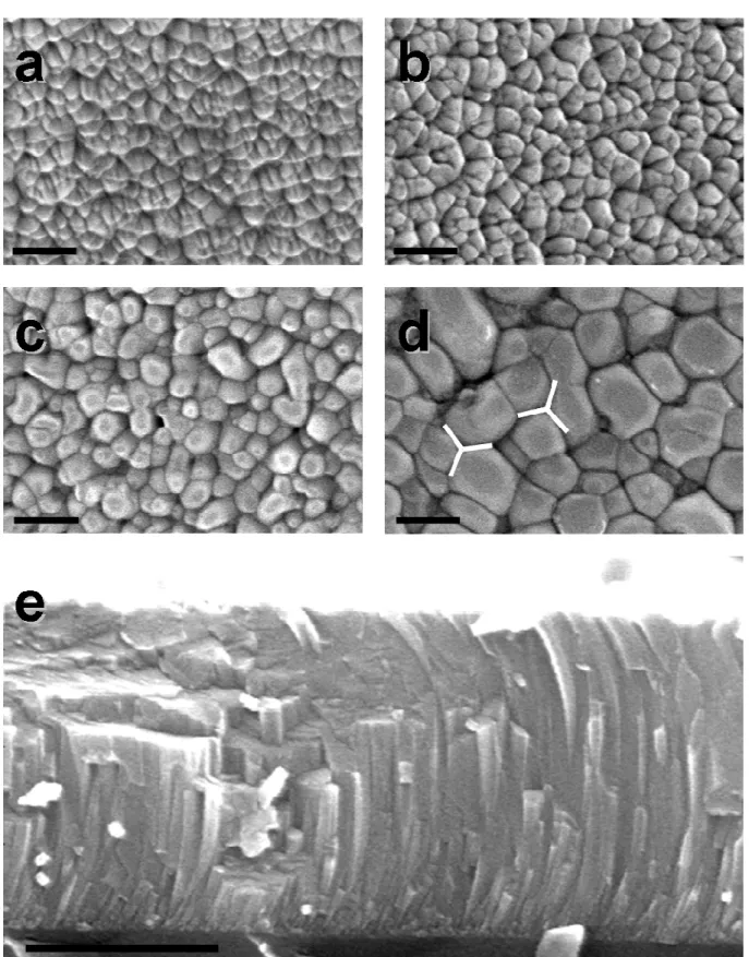
Figure 1 a-d presents top views of the surface of the AZO films obtained by SEM, before (a) and after thermal annealing during 300 s at Ta=650 °C (b), 800 °C (c), and 900 °C (d). The
as-deposited film is well crystallized with an average grain size of 40 nm. Figure 1e presents a side view of the as-deposited film. The film is about 750 nm thick and presents a columnar structure with a lateral size of the columns of the order of 40 nm, which is consistent with the top view.21 The columns are not perfectly straight because the substrate is moving under the target in the magnetron chamber during the sputtering deposition. At the beginning of the sputtering, the substrate is not under the target and the flux of atoms arrives at the surface under an angle, which results in the tilt of the columns. Upon translation, the substrate arrived right under the target, and no angle is observed. Finally, when the sample is far away from the target a tilt in the other direction is observed. Thermal annealing at temperatures lower than 750 °C does not induce modifications of the surface morphology and grain size (Fig. 1b). At 800°C, the grains start growing and an average grain size of 60 and 100 nm is observed after thermal annealing at 800 °C and 900 °C respectively. Moreover, the geometry of the grain is also affected by the annealing and a faceting of the grains is observed, with the formation of a 120 ° angle at the boundary between three grains (shown on Figure 1d). This increase of the grain size and the modifications in the grain morphology may be induced by Ostwald ripening; zinc oxide diffusion becomes significant at temperatures higher than 800°C and allows for the formation of larger grains.22
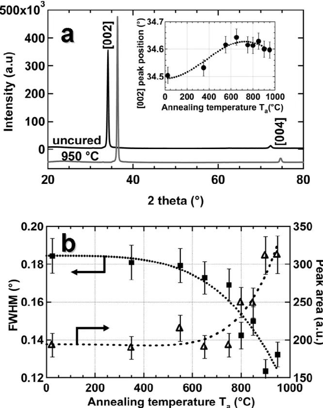
The crystalline structure of the samples was further investigated by X-ray diffraction (XRD). Figure 2a presents the diffraction patterns of the films before and after annealing at 950 °C. The diffraction patterns are dominated by a peak at around 34.5 ° and a smaller one at
74 °. These peaks are respectively assigned to the [002] and [004] orientations,23 demonstrating the marked texture of the film along the c-axis of the hexagonal structure in complete agreement with the columnar structure observed by SEM. The inset on Fig. 2a shows the position of the [002] peak after annealing at various temperatures for ta=300 s. A
progressive shift to higher 2θ value is observed even at relative low temperatures. It has been previously shown that, after the deposition, the AZO layers are in slight compression.24 This initial compressive stress along with the compressive thermal stress is relaxed during annealing, due to the formation of a larger crystalline phase. After full thermal treatment the residual stress is tensile, resulting in the shift shown on Fig. 2a.25
Another evidence of the modification of the crystalline structure is obtained from the shape of the XRD peaks. Figure 2b presents the peak area and the full-width at half-maximum (FWHM) for the [002] peak after annealing at various temperatures. As Ta increases, the
FWHM decreases, reflecting an increase in the grain size.26 Very little variations are observed for Ta<750 °C, while the grain size increases significantly above 800 °C, as previously
demonstrated on Fig 1. On the other hand, At 800 °C (resp. 900 °C), the peak intensity increases by 25% (resp. 60%). This shows the formation of a larger crystalline phase inside the materials.
3.2 Effect of annealing temperatures on the optical properties
The electronic properties of the ZnO samples can be derived from the optical transmission spectrum. The gap energy can be measured using the following formula:27
Ahν=C·(Eg-hν)1/2 (1)
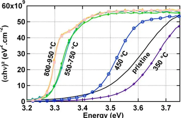
where α is the absorption coefficient of the sample, h the Planck constant, ν is the frequency of the incident light, Eg the gap energy and C a constant. Figure 3 presents the
evolution of (αhν)² as a function of the photon energy hν. For the as deposited sample, the absorption is not sharp and the gap energy is 3.42 eV. After thermal annealing at 350 °C, the gap increases to 3.54 eV. For thermal annealing at higher temperatures, the gap progressively shifts to lower values to finally reach Eg= 3.27 eV. A first possible explanation is a
Moss-Burnstein shift due to the progressive reduction of the charge carrier density inside the material with the thermal annealing. In the initial state, the presence of electron donors leads to an increase of the optical gap: as the first levels of the conduction band are already filled, electrons from the valence band need more energy to reach the first unoccupied levels in the conduction band.28 Upon annealing at 350 °C, the Al-dopants are activated leading to a slight blue shift of the optical band gap. This effect has already been observed for magnetron sputtered AZO thin films and is consistent with an increase in the film electrical conductivity.29
During annealing at temperatures higher than 450 °C, the charge density decreases; this empties the lower levels of the conduction band and could explain the reduction of the absorption edge energy. To further study the origin of the absorption edge shift, the sample annealed at 950 °C under Argon was further annealed at 450 °C for one hour but under hydrogen. Hydrogen is known as reductant and leads to an increase of the charge carrier density.19 Figure 4 presents (αhν)² as a function of the photon energy for the sample annealed under Argon and the one subsequently annealed under H2. A very small shift of the absorption
band edge of 10 meV is observed after the reductive treatment. This shift is more in agreement with the values commonly found for semiconductor doping.13 Therefore, the Moss-Burnstein shift is not the main reason of the modification of the absorbance spectra above 450 °C.
Recent XANES studies suggest another explanation for the absorption modifications. Increasing the substrate temperature for magnetron sputtering AZO films leads to the
formation of secondary phases of insulating ZnO and ZnAl2O4 from Al2O3(ZnO)3
homologous phase.30-31 In our experiments, annealing at 450 °C and above, gives enough energy at the Al atoms to allow for diffusion and therefore segregation. The Al segregation leads to a different material and so to another band structure. This explains why a very large red-shift of the absorption edge is observed with a final value closed to the optical band gap of pure ZnO.
Annealing also affects the shape of the absorption edge. For annealing above 800 °C, a transition in the absorption edge is observed with a higher slope and a shoulder in the absorption around 3.32 eV. This shoulder may be assigned to the first exciton of ZnO.2 Finally, the position of the gap in the near UV associated with the sharp absorption edge leads to a high transmission of the sample. After thermal annealing, even at low temperatures, the optical transmission can reach 82%. The overall transmission is limited by the reflection at the air/AZO interface due to the high index of AZO.
3.3 Photoluminescence properties of AZO samples
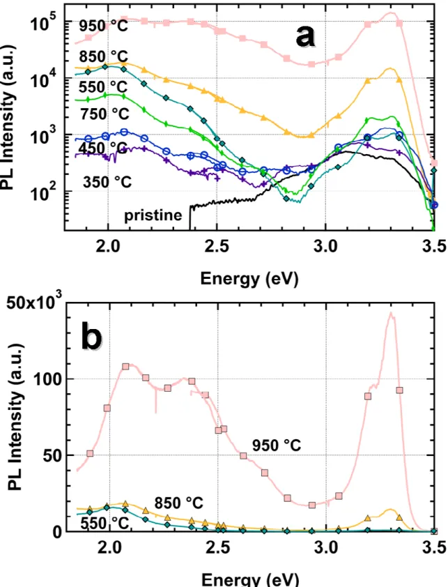
Figure 5 presents the photoluminescence (PL) spectra of the samples after annealing at various temperatures. The spectra were plotted in a log-scale to emphasize the strong increase of the PL intensity with thermal annealing. All the spectra present the two main luminescence contributions: the near band edge emission around 360-400 nm and the “orange emission” between 450 and 650 nm. The overall intensity, the ratio between these two contributions, and the shape of the peaks show a strong dependence on Ta. Before annealing (black curve), the
AZO sample presents a very weak luminescence and the signal is in the UV range. When the annealing temperature is increased, the near band edge emission increases and is progressively shifted to higher energy. Due to the increase of the grain size after annealing,
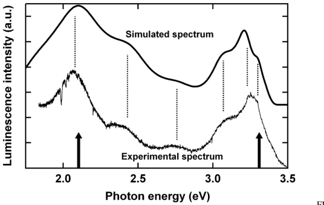
the chances of non-radiative recombination are reduced and the PL signal is increased. Above 650 °C, the near band edge emission presents two peaks at 380 and 390 nm. This type of splitting was already reported for the study of room temperature cathodoluminescence of ZnO thin films.32 Actually, this is not a real splitting. The double peak structure can be simply explained by Fabry-Perot fringes. . Indeed, this can be further evidenced at lower energy where the oscillations of the transmission spectra correspond to the modulation of the PL signal. To confirm this effect we simulated the luminescence by simply multiplying the transmission spectrum with two Gaussian peaks, one for the near band edge emission at 375 nm and the other to account for defect emission centered at 590 nm. The result is shown on Figure 6. Dashed lines correspond to local maxima and illustrate the very good agreement between the experimental data and the simulated spectrum.
For annealing temperatures greater than 800 °C, a strong increase of the overall intensity and more specifically the near band edge emission is observed. After annealing at 800 °C and 900 °C, the intensity of the near band edge emission is respectively 8 and 80 times higher than after annealing at 750 °C. The increase of the grain size observed previously with SEM and XRD explains the strong increase of the near band edge emission. For larger grains, the chance of a non-radiative recombination of the exciton on defect at the grain boundary is reduced and therefore the PL signal is increased.
Furthermore, the orange emission strongly increases with Ta and indicates the creation of
interstitial oxygen. 33 This observation is a further evidence of the atom diffusion and phase segregation inside the materials. To heal the defects created by the phase segregation and control the ratio orange/visible emission, subsequent annealing into H2 atmosphere was
performed. The reductive annealing leads to an increase of the ratio UV emission vs. visible emission of a factor 5.
The emission color was measured according to the standards of the Commission Internationale de l’Eclairage, (CIE) as defined in 1931.34 The tristimulus values X, Y, and Z were obtained by convolving the emission spectra with the three Standard Colorimetric Observers. The chromaticity of the sample annealed at 950 °C were x=0.383 and y=0.437. These values are reported on the Figure 7. Clearly, the luminescence of the sample is set in the white region and is less orange than previously reported values for doped ZnO films.8 To further characterize this white emission, the corresponding color temperature was calculated from the x, and y values and was found equal to 4500 K. This is significantly higher than incandescent light bulb values, meaning a cooler light with a less yellowish contribution. The presence of a broad and significant near band edge emission around 390 nm explains why such a high value is found for the color temperature.
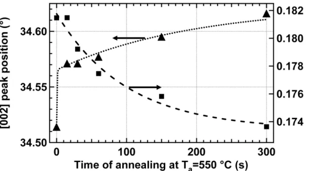
3.4 Investigation of the Al segregation at 550°C
The Al segregation at low temperature can be further investigated by varying the annealing time to follow the kinetics. Samples were annealed at 550°C for various times ranging from 15 to 300 s. Annealing at 550°C seems to be a good compromise between the need of a rapid annealing and a sufficiently slow kinetics to observe the variations. Figure 8 presents the FWHM and the position of the [002] peak in XRD experiments on the AZO thin films after annealing at 550 °C. The [002] peak shifts to higher 2-θ value even for very short annealing time and shows little increase for longer annealing. Even for short ta, the residual
compressive stress after deposition can relax easily during the annealing and the beginning of the cooling phase. After cooling, this leads to a final tensile stress and a shift of the XRD peak. The FWHM shows little decrease during the annealing; this evidences the limited impact of annealing at low temperature on the crystalline structure of the films.
Figure 9 shows the evolution of the optical band gap, measured from the absorption of the sample (see Fig. 3). The same progressive reduction of the band gap due to the partial Al segregation of the films is observed. The values of the normalized visible emission, defined as the ratio of the “orange emission” to the near band edge UV emission; is also reported in Figure 9. This normalized visible emission increases strongly during annealing. To better understand the link between the PL spectrum and the optical properties, the normalized visible emission is given on Figure 10 as a function of the gap energy. The results confirm the crucial role of phase segregation in the optical and luminescence properties of the AZO thin films and demonstrate how a fine control over the annealing conditions enables the tuning of the emission properties.
4. Conclusions
AZO films were deposited with magnetron sputtering. The impact of Rapid Thermal Annealing was investigated in close connection with structural, optical and electronic properties. During annealing, two phenomena occur in different temperature ranges. Between 350 and 550 °C, phase segregation occurs inside the layer, as assessed by the gap shift and the increase of visible luminescence. A kinetics study shows the relation between the intensity of visible luminescence and the shift of the gap. Above 800 °C, there is an increase of the crystalline phase and grain size, as demonstrated by XRD and SEM. This increase leads to an overall increase of the luminescence and specifically of the UV peak. It is then possible to modify the PL spectrum of AZO thin films to obtain efficient white emission.
Acknowledgements
The authors thank Daniel Abriou for the SEM picture and Mohamed Selmane for assistance with XRD experiments.
References
[1] F. Porter, Zinc Handbook: Properties, Processing, and Use in Design. CRC Press, 1991 [2] Y. Chen, D. M. Bagnall, H. J. Koh, K. T. Park, K. Hiraga, Z. Zhu, J. Appl. Phys. 84 (1998) 3912
[3] N. E. Hsu, W. K. Hung, Y. F. Chen, J. Appl. Phys 96 (2004) 4671-4673 [4] M. D. Mccluskey, S. J. Jokela, J. Appl. Phys. 106 (2009) 071101
[5] A. Che Mofor, A. El-shaer, A. Bakin, A. Waag, Appl. Phys. Lett. 87 (2005) 062501 [6] M. Joseph, H. Tabata, and T. Kawai, Appl. Phys. Lett. 74 (1999) 2534
[7] X. Jiang, F. L. Wong, M. K. Fung, and S. T. Lee, Appl. Phys. Lett. 83 (2003) 1875 [8] S. Müller, M. Lorenz, C. Czekalla, G. Benndorf, H. Hochmuth, M. Grundmann, H. Schmidt, C. Ronning, J. Appl. Phys.104 (2008) 123504
[9] N. Ohashi, T. Nakata, T. Sekiguchi, H. Hosono, M. Mizuguchi, T. Tsurumi, J. Tanaka, H. Haneda, Jpn. J. Appl. Phys. 38 (1999) L113.
[10] M. Wang, E. Woo, S. Jin, S. Chung, K. Koo, J. Mater. Sci. 45 (2010) 4111
[11] N. Ohashi, N. Ebisawa, T. Sekiguchi, I. Sakaguchi, Y. Wada, Appl. Phys. Lett. 86 (2005) 091902
[12] S. Kuo, W. Chen, F. Lai, C. Cheng, H. Kuo, S. Wang, W. Hsieh, J. Cryst. Growth 287 (2006) 78
[13] Y. Sobajima, S. Kato, T. Matsuura, T. Toyama, H. Okamoto, J. Mater. Sci.: Mater Electron. 18 (2007) 159
[14] K. K. Kim, H. Tampo, J. O. Song, T. Y. Seong, S. J. Park, J. M. Lee, S. W. Kim, S. Fujita, S. Niki, Jpn. J. Appl. Phys. 44 (2005) 4776
[15] M. Cui, X. Wu, L. Zhuge, Y. Meng, Vacuum 81 (2007) 899 [16] G. Fang, D. Li, B. Yao, Thin Solid Films 418 (2002) 156
[17] M. Wang, K. E. Lee, S. H. Hahn, E. J. Kim, S. Kim, J. S. Chung, E.W. Shin, C. Park, Mater. Lett. 61 (2007) 1118
[18] Y.J. Lin, W. C. Chen, H. C. Chang, C. J. Liu, Z.R. Lin, J Cryst. Growth 310 (2008) 4110 [19] J. H. Noh, H. S. Jung, J. K. Lee, J. Y. Kim, C. M. Cho, J. S. An, K. S. Hong, J. Appl.
[20] S. Hu, Y. Lee, J. Lee, J. Huang, J. Shen, W. Water, Appl. Surf. Sci. 254 (2008) 1578 [21] Y. Zhou, P. J. Kelly, A. Postill, O. Abu-Zeid, A. A. Alnajjar, Thin Solid Films 447 (2004) 33
[22] S. T. Tan, X. W. Sun, X. H. Zhang, S. J. Chua, B. J. Chen, C. C. Teo, Jpn. J. Appl. Phys. 100 (2006) 033502
[23] Joint Comitee on Powder Diffraction Standards, Powder Diffraction File 036-1451 [24] F. Conchon, P.O. Renault, P. Goudeau, E. Le Bourhis, E. Sondergard, E. Barthel, S. Grachev, E. Gouardes, V. Rondeau, R. Gy, Thin Solid Films 518 (2010) 5237
[25] V. Hauk, Structural and Residual Stress Analysis by Nondestructive Methods, Elsevier, 1997
[26] H. P. Klug, L. E. Alexaander, X-ray diffraction procedure for crystalline and amorphous materials, Wiley, New York, 1974
[27] E. Ziegler, A. Heinrich, H. Oppermann, G. Stover, Phys. Stat. Sol. A 66 (1981) 635 [28] G H Lee, Y Yamamoto, M Kourogi, M Ohtsu, Thin Solid Films 386 (2001) 117-120 [29] S. Cornelius, M. Vinnichenko, N. Shevchenko, A Rogozin, A Kolitsch, W. Möller, Appl. Phys. Lett. 94 (2009) 042103.
[30] S. Yoshioka, F. Oba, R. Huang, I. Tanaka, T. Mizoguchi, T. Yamamoto, J. Appl. Phys. 103 (2008) 014309.
[31] S. Cornelius, M. Vinnichenko, N. Shevchenko, a Rogozin, a Kolitsch, W. Möller, Applied Physics Letters 94 (2009) 042103
[32] M. Lorenz, R. Johne, T. Nobis, H. Hochmuth, J. Lenzner, M. Grundmann, A.P.D.
Schenk, S.I. Borenstain, A. Schön, C. Bekeny, T. Voss, and J. Gutowski, Appl. Phys. Lett. 89 (2006) 243510
[33] C Chandrinou, N Boukos, C Stogios, and A Travlos, Microelectronics Journal 40 (2009) 296-298
Figure captions
FIG. 1. SEM images of AZO thin films. a-d: top view of the surface before (a) and after annealing during 300 s at Ta=650 °C (b), 800 °C (c), and 900 °C (d). The scale bar is 200 nm.
FIG. 2 (A) X-Ray Diffractogramm of AZO samples before and after annealing at 950°C for 300 s. The curve at 950 °C was right-shifted for clarity. Inset: [002] peak position after annealing at various temperatures for 300 s. (B) Full-width at half-maximum (square) and area (triangle) for the [002] peak.
FIG. 3 (αhν)² as a function of the photon energy hν, (α is the absorption coefficient) for AZO samples annealed under argon at various temperatures for 300 s. The absorption coefficient was measured with a UV-Vis spectrophotometer.
FIG. 4 (αhν)² as a function of the photon energy hν, (α is the absorption coefficient) for AZO samples annealed under argon at 950 °C for 300 s (red line), and subsequently annealed one hour at 450 °C under hydrogen (blue line). The absorption coefficient was measured with a UV-Vis spectrophotometer.
FIG. 5 Photoluminescence intensity as a function of the photon energy hν, for AZO samples annealed under argon at various temperatures for 300 s, in a logarithmic (a) and linear (b) scales. The PL spectra were collected under normal incidence with an excitation energy of 3.8 eV (325 nm).
FIG. 6
Bottom: Experimental luminescence after annealing at 450 °C. Top Simulated spectrum
obtained from the sum of two Gaussian peaks (respective positions are indicated by the arrows) multiplied by the transmission. The dashed lines illustrate the coincidence of the local maxima.
FIG. 7 Chromaticity of the emission of the AZO film annealed at 950 °C as reported in the color map defined with the CIE 1931 standards
FIG. 8 X-Ray Diffraction experiments on AZO thin films before and after annealing at 550 °C for various time ta. Full-width at half-maximum (square) and position (triangle) for the
[002] peak.
FIG. 9 AZO thin films annealed under argon at 550 °C for various annealing times. Optical gap energy (triangles) measured from the absorption coefficient and ratio between the visible and the UV peaks (square) in PL experiments as a function of the annealing time.
FIG. 10 AZO thin films annealed under argon at 550 °C for various annealing times. Optical gap energy as a function of the normalized visible PL intensity..