HAL Id: hal-02997067
https://hal.archives-ouvertes.fr/hal-02997067
Submitted on 9 Nov 2020
HAL is a multi-disciplinary open access
archive for the deposit and dissemination of
sci-entific research documents, whether they are
pub-lished or not. The documents may come from
teaching and research institutions in France or
abroad, or from public or private research centers.
L’archive ouverte pluridisciplinaire HAL, est
destinée au dépôt et à la diffusion de documents
scientifiques de niveau recherche, publiés ou non,
émanant des établissements d’enseignement et de
recherche français ou étrangers, des laboratoires
publics ou privés.
To cite this version:
Niyazi Ulas Dinc, Demetri Psaltis, Daniel Brunner. Optical neural networks: The 3D connection.
Photoniques, EDP Sciences, 2020, pp.34-38. �10.1051/photon/202010434�. �hal-02997067�
FOCUS
PHOTONICS AND ARTIFICIAL INTELLIGENCE
///////////////////////////////////////////////////////////////////////////////////////////////////
OPTICAL NEURAL NETWORKS:
THE 3D CONNECTION
We motivate a canonical strategy for integrating
photonic neural networks (NN) by leveraging 3D printing.
Our belief is that a NN’s parallel and dense connectivity is
not scalable without 3D integration. 3D additive fabrication
complemented with photonic signal transduction can
dramatically augment the current capabilities of 2D CMOS
and integrated photonics. Here we review some of our
recent advances made towards such an architecture.
Niyazi Ulas DINC
1, Demetri PSALTIS
1, Daniel BRUNNER
2,*1 Optics Laboratory, École Polytechnique Fédérale de Lausanne, Lausanne, Switzerland
2 FEMTO-ST/Optics Department, UMR CNRS 6174, Université Bourgogne Franche-Comté, 25030 Besançon Cedex, France
https://doi.org/10.1051/photon/202010434
This is an Open Access article distributed under the terms of the Creative Commons Attribution License (http://creativecommons.org/licenses/by/4.0), which permits unrestricted use, distribution, and reproduction in any medium, provided the original work is properly cited.
S
everal decades passed between the introduc-tion and the large-scale exploration of neural networks (NN). Since the proposal of simple NNs in 1943 [1], the field has gone through multiple cycles of euphoria and challenges until reaching today’s large-scale interest and exploitation [2]. Readily available high-perfor-mance computing systems now al-low emulating powerful (deep) NN architectures whose connections are optimized based on computational-ly expensive learning concepts such as gradient back-propagation. As a consequence, NN currently excel on previously unseen scales, but at the same time the constraints of today’s CMOS-based computing threatens to limit the reach of this revolution.As illustrated by their name, the initial objective of NN, cf. Fig. 1(A), was providing a ‘logical calculus of
the ideas immanent in nervous ac-tivity’ [1], and as such their compo-sition mirrors a most rudimentary aspect of the mammalian neo-cor-tex: nodes are densely linked into a network with connections much like synapses, dendrites and axons connecting biological neurons. However, this is only possible in the context of a global structural property of the neocortex in which neurons, and even more so connec-tions, are distributed across a 3D volume, cf. Fig. 1(B). The majority of cortical neurons are arranged in planes located inside the grey mat-ter that wraps around the brain, and stacks of neurons form short-range connections (labelled a in Fig. 1(B)) which travers the grey matter’s vo-lume. Crucially, grey matter encloses white matter, and inside this volume the brain’s long-range (connections (labelled b and c in Fig. 1(B)) connec-tions are located. 3D connecconnec-tions
are therefore a canonical feature of brain architecture. The scale and connectivity of the human brain’s network would otherwise simply not fit inside the human skull. The brain therefore provides a very good pri-mer for exploiting 3D circuit topolo-gy. Even though the 3D topology of brains emerged from evolutionary development, science and enginee-ring can deliberately combine ad-vantageous strategies and concepts. Combining the 3D network topology of biological brains with photonic signal transduction is a highly ap-pealing strategy for next generation NN computing.
In this paper, we elaborate the po-tential of 3D printing technology for integrated photonic NN chips. Such additive fabrication enables true 3D integration and naturally comple-ments the mostly 2D lithography that struggles to implement parallel NN connections with a scalable strategy.
Photonics offers fundamental energy, speed and latency advantages when es-tablishing the communication between NN neurons along the staggering amount of network connections. 3D printing is a potential path for 3D integration of op-tically interconnected Si or other elec-tro-optic chips.
CANONICAL 3D PHOTONIC NEURAL
NETWORK ARCHITECTURE
Physically realizing dense connections for the large number of neurons (typi-cally >1000 units) contained in each NN layer results in a formidable challenge. A parallel NN processor needs to pro-vide a dedicated physical link for each connection, which is difficult since the amount of possible connections scales quadratically with the number of neu-rons. A connection’s defining property is its strength, and its physical imple-mentation for example by memristors, micro-rings or holographic memory always occupies some basic unit of area
i.e. volume. Integration in 2D results in
a quadratic scaling of the circuit’s area with a network’s size [3], cf. Fig. 2(A). In a 3D implementation weights can be stacked, for example, in planes, and for the simplest organization [3], both, the number of required planes and me-mory-elements per plane scale linearly with the number of neurons. This miti-gates the size-scalability roadblock and 3D routing may well be a fundamental
prerequisite for scalable and parallel NN chips. Realizing such 3D circuits electro-nically is challenging due to the capaci-tive coupling and the associated energy dissipation when sending information along signalling wires.
In order to overcome these challen-ges we investigated a canonical photo-nic NN architecture where neurons in the form of nonlinear components are arranged in 2D sheets, while connec-tions are integrated in 3D printed photonic circuits, cf. Fig. 2(B). We do not constrain the nature of photonic neurons or the 3D routing strategy. All-optical as well as electro-optical components acting as neurons are possible, and the 3D photonic inter-connect can be realized by refractive index modifications in a 3D medium, multiple stacks of diffractive-optics pla-nes [4] as well as complex 3D circuitry of photonic waveguides [3].
3D NANO-PRINTING TECHNOLOGY
Additive manufacturing (AM) has been a popular method for prototyping ever since it was developed in the 1980s as it does not require special tooling or molds. However, its true advantage over most conventional manufacturing methods is AM’s ability to produce 3D parts of great complexity, which is unfeasible or even impossible with subtractive or 2D litho-graphic methods. Among various AM techniques, two-photon polymerization
Figure 1.
(A) In a Neural Network (NN) typically millions of connections link simple nonlinear neurons which are arranged in layers. (B) In the brain short, medium and long range (a, b, c, respectively) neural connections are established in the volume of white and grey matter. Adapted from Schüz, et al., Encyclopedia of Neuroscience 2009.
Over the past de-cade, photonic device integra-tion has grown exponentially. Demanding opti-cal systems such as ADAS camera modules, AR/VR headsets, and smartphone camera lenses are pushing the limits of optical design and manufacturing. With larger fields of view and broader wave-length ranges, the lens parameters are constantly improving. One of the challenges for manufacturers is to qualify ever more complex lenses with the highest accuracy even though traditional metrolo-gy instruments reach their limits. By working in close collabora-tion with manufacturers, Phasics pushes optical testing limits and proposes a new metrology tool dedicated to the qualification of demanding assemblies. KALEO MTF is an automatic test station designed to provide complete lens qualification on-and-off axis at multiple wavelengths: wavefront error, Modulation Transfer func-tion (MTF), trough-focus MTF as well as geometric and radiometric lens parameters. KALEO MTF is the dedicated solution for optical desi-gners in search of efficient prototy-ping and production teams looking for fast and accurate quality control and troubleshooting. CONTACT PHASICS +33 (0) 1 80 75 06 33 [email protected] www.phasicscorp.com
UNRIVALED WIDE
ANGLE LENS TEST
WITH KALEO MTF
AD
VER
FOCUS
PHOTONICS AND ARTIFICIAL INTELLIGENCE
(TPP) is of special interest since it provides sub-micron feature sizes in materials that are transparent in the optical domain with refractive index values close to those of glass. TPP utilizes femtosecond lasers to expose and polymerize photore-sists. The two-photon process is of significance as it enables feature sizes below the Abbe diffraction li-mit thanks to the polymerization’s quadratic dependence on exposure intensity. One-photon processes in turn yield larger polymerized voxels due to a linear dependence of polymerization on exposure in-tensity. Control of the light intensity threshold for polymerization and quenching effects further contri-bute to sub-diffraction resolution. TPP exposure-dose can be controlled through scanning speed and laser in-tensity, which provides control over the degree of photoresist's polyme-rization and hence over the local refractive index. This enables the possibility of printing graded-index
(GRIN) elements [5]. 3D direct-laser writing systems offer robust, com-mercial TPP setups where complex optical elements can be printed (cf. Fig. 3) at different resolutions by selecting among different resin-ob-jective pairs. In subsequent sections, we present different optical elements that were fabricated by a Nanoscribe 3D printer.
For the concepts presented in this paper, the most important feature of AM/TPP is the ability to access independently each voxel in the fabrication volume, which enables holographic as well as wave-guide based photonic connections. From the holography point of view it is key to go beyond 1/M2, which is the
ef-ficiency relation where M is the nu-mber of multiplexed holograms [6]. This fundamental limitation holds for any optical holographic material where recording is accomplished by means of multiple optical expo-sures [7] due to the superposition of multiple holograms following a recording sequence that is designed to use the dynamic range of the in-dex modulation equally. Crucially, efficiency could be improved to 1/M if the hologram were constructed voxel-by-voxel or in a multilayered fashion. TPP makes it practical to adopt both options. In addition, the ability to access each point in the volume enables the fabrication of complex 3D-routed waveguides that define the optical signal’s path in 3D, reminiscent of the dendrites and axons in the brain.
3D DISCRETE-WAVEGUIDE
INTERCONNECTS
As previously introduced, connec-tions between biological neurons are made by dedicated ‘wires’ formed by axons connected to dendrites via
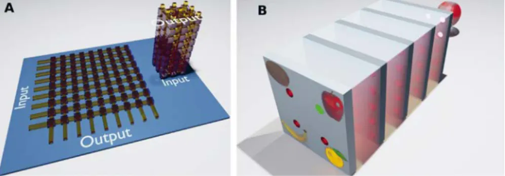
Figure 2.
(A) Realizing the connections in 2D interconnects is not scalable, and 3D integration is essential for parallel NN integration. (B) In our canonical 2D/3D photonic NN, neurons are arranged in 2D while connections are established in the 3D volume between layers of neurons, where the NN correctly identifies an apple.
Figure 3.
(A) 3D printing scheme with the objective focusing the femtosecond laser pulse into the photoresist. (B) Layer-by-layer printing process.
synapses, and the photonic equivalent of such spatially discrete links is the optical waveguide. An optical waveguide utilizes the principle of total internal reflection, where a medium with a higher refrac-tive index is surrounded by a medium with a lower refractive index. Recently Moughames et al. [3] 3D printed such optical waveguides using a Nanoscribe 3D printer and connections in the form of optical splitters realized the dense connectivity between neurons.
Different connection topologies were demonstrated. Arranging 1 to 81 split-ters in an 15×15 input waveguide array,
cf. Fig. 4(A), demonstrated a 3D printed
dense interconnect for 225 neurons in an area of only 300×300 µm2. Inspired
by convolutional NNs, the same authors realized Boolean Haar filters arranged in a 7×7 array, see Fig. 4(B). Such ar-rays can filter images containing 21×21 pixels in parallel, which in principle is sufficient for realizing a convolutional layer applied to the MNIST handwritten digit dataset. Most importantly the area of both 3D interconnects scales linearly with the number of inputs.
GRADIENT INDEX CONTINUOUS
INTERCONNECTS
Multilayered diffractive optical ele-ments, cf. Fig. 5, can also perform in-terconnection tasks utilizing the 3D via optical volume elements (OVEs). OVEs can be designed by utilizing a nonli-near optimization scheme, learning
tomography (LT), which calculates the topography of either multilayered or GRIN volume elements to approximate desired mappings. Figure 5(A,B) shows an demonstration by Dinc et al., which acts as an angular multiplexer (lantern) that maps plane waves with different incidence angles to linearly polarized multimode fiber modes [4]. It provides an interconnect between single mode fibers stacked with different angles and a multi-mode fiber to map each single multi-mode fiber input/output to a specific mode of multi-mode fiber, hence performs multi- mode-divi-sion multiplexing. Another example of LT computed OVEs realizing Haar filters such as demonstrated in [3] are shown in Fig. 5(C,D).
POSSIBILITIES
FOR PHOTONIC NEURONS
The function of a NN neuron is the summation of its inputs followed by a nonlinear transformation. Summation of the individual fields impinging on a neuron can be realized in photo-nics by the superposition of optical fields. Unfortunately, nonlinearity is since many years the Achilles-heel of photonics compared to electronics. However, modern photonic devices have significantly lowered the energy consumption which can now be below 100 fJ per nonlinear transformation [8]. Many standard nonlinear photo-nic components have potentially high modulation bandwidths, fast response
Figure 4.
SEM micrographs of 3D printed waveguides [3] realizing parallel interconnects with high connectivity (A) and according to Haar filters (B).
FOCUS
PHOTONICS AND ARTIFICIAL INTELLIGENCE
times and can directly be interfaced with fully parallel as well as dense 3D photonic interconnects. Photonic neurons combined with our 2D/3D canonical NN architecture therefore offer new concepts for addressing the long-standing challenges of pa-rallelism and connection density for high-speed NN computers.
In order to make most effi-cient use of the footprint and cir-cuit volume, photonic neurons need to be arranged in a 2D array. Furthermore, neurons that accept multi-mode fields as their input could potentially be beneficial as this relaxes design constraints and allows for high-density integration of 3D photonic waveguides without a cladding. Finally, any optical trans-formation is associated with losses and the 3D photonic interconnect is no exception; neurons including optical amplification would mitigate such losses. At this stage, we can imagine all-optical, electro-optical as well as plasmonic neurons, and the most promising concept will certainly have to strike a balance between speed, efficiency, flexibility and potentially amplification.
OUTLOOK
The viability of integrating photonic circuits suited for NN interconnects in 3D has recently been demons-trated in principle [3, 4]. Ultimately, scalability is key for computing hard-ware, which implies that stacking 2D neurons and 3D interconnects into deep photonic NNs requires optical
losses to be counterbalanced by am-plification without resulting in an unsustainable thermal energy de-position inside the integrated pho-tonic circuit.
However, the computational power of a NN relies on more than simply establishing specific
connections in parallel. The non-linearity of its neurons is a fun-damental requirement for solving complex tasks, and here signifi-cant room for improvement exists. Another defining feature of NN is the optimization of their connec-tions during training. New, ideally in-situ optimization strategies are in urgent demand. In combination with plasticity such as non-volatile memristive effects, these concepts would significantly reduce the com-plexity of potential auxiliary sup-port circuits as well as of the 3D interconnect itself.
ACKNOWLEDGMENT
This work was supported by the EUR EIPHI program (Contract No. ANR-17-EURE-0002), the Volkswagen Foundation (NeuroQNet I&II).
REFERENCES
[1] W.S. McCulloch, W. Pitts, Bull. Math. Biophys. 5, 115 (1943) [2] Y. LeCun, Y. Bengio, G. Hinton, Nature 521, 436 (2015) [3] J. Moughames et al., Optica 7, 640 (2020)
[4] N.U. Dinc, J. Lim, E. Kakkava, C. Moser, D. Psaltis, Nanophotonics (2020) [5] A. Žukauskas, I. Matulaitiene, D. Paipulas et al., Laser Photonics Rev. 9, 706 (2015) [6] D. Psaltis, D. Brady, X.-G. Gu, and S. Lin, Nature 343, 325 (1990)
[7] G. Barbastathis, D. Psaltis, Holographic Data Storage, in Holographic Data Storage, 2000, pp. 21–42
[8] T. Heuser, M. Pflüger, I. Fischer, J.A. Lott, D. Brunner, S. Reitzenstein, J. Phys. Photonics 2, 044002 (2020)
Figure 5.
(A) 3D rendering of the OVE in [4] with the ideal input and output pairs; (B) SEM image of the printed structure and the corresponding experimental results. (C) XY, YZ and XZ cut planes of a GRIN OVE, optimized for Haar filtering. The colorbar shows RI variation. (D) Corresponding output fields obtained by simulating the propagation of inputs through the optimized GRIN volume. All field plots have a window size of 32x32 μm2 and color code