HAL Id: tel-00090546
https://tel.archives-ouvertes.fr/tel-00090546
Submitted on 31 Aug 2006
HAL is a multi-disciplinary open access
archive for the deposit and dissemination of sci-entific research documents, whether they are pub-lished or not. The documents may come from teaching and research institutions in France or abroad, or from public or private research centers.
L’archive ouverte pluridisciplinaire HAL, est destinée au dépôt et à la diffusion de documents scientifiques de niveau recherche, publiés ou non, émanant des établissements d’enseignement et de recherche français ou étrangers, des laboratoires publics ou privés.
Dots:Electronic Polarons and Excitonic Polarons
Vanessa Preisler
To cite this version:
Vanessa Preisler. Carrier LO Phonon Interactions in InAs/GaAs Quantum Dots:Electronic Polarons and Excitonic Polarons. Physics [physics]. Université Pierre et Marie Curie - Paris VI, 2006. English. �tel-00090546�
by Vanessa Preisler
A Thesis Presented to
L’Universit´e Pierre et Marie Curie (Paris VI) In Partial Fulfillment of the Requirements
for the Degree of Doctor of Philosophy
´
ECOLE NORMALE SUP´ERIEURE D´EPARTEMENT DE PHYSIQUE
Paris, France 2006
This thesis presents a study of electrons, holes and excitons confined in self-assembled InAs/GaAs quantum dots. The interaction of these confined carriers with the lon-gitudinal optical (LO) phonons of the surrounding crystal lattice is investigated. It is found that this interaction leads to the formation of the so-called quantum dot polarons; hybrid carrier phonon states which are the true excitations of a charged dot.
The first part of this thesis describes the results of far infrared (50 - 700 cm−1)
magnetospectroscopy experiments performed on n- and p-doped samples. The intra-band energy levels of these systems are probed. The magnetic field is an important experimental parameter, as it allows for the evolution of the energy levels, necessary for the observation of electronic and hole polaron levels. Using the Fr¨ohlich Hamil-tonian, which couples the phonon and purely electronic states, the energy levels and oscillator strengths of the system are determined. For both the investigation of elec-trons and holes confined in dots, a good agreement is found between the calculations and the experimental results.
The second part of this thesis is dedicated to the study of the interaction between electron-hole pairs or excitons and the phonons of the lattice. The interband en-ergy transitions of the dots are investigated using photoluminescence excitation and resonant photoluminescence spectroscopy under strong magnetic fields up to 28 T. These techniques allow for the circumvention of the inhomogeneous broadening of the resonances that arise from size and composition fluctuations in the quantum dot ensembles. The magnetic field dependence of the resonance energies allows for an unambiguous assignment of the interband transitions. The excitonic polaron energies as well as the oscillator strengths of the interband transitions are determined. The calculations account well for the experimental data.
No matter how hard I tried, it was impossible to be a stressed out Ph.D. student with a thesis advisor like Yves Guldner. Any problem, fear or doubt I could come up with, Yves was always there to reassure me and find a solution. Along with making sure that every aspect of my graduate school experience in France went smoothly, he, being the ultimate source on semiconductor physics, has been a wonderful teacher for me throughout these past three years.
Most Ph.D. students count themselves lucky if they have one capable theorist with whom they can work. With Robson Ferreira and Gerald Bastard across the hall from me during these past three years, I had two gifted theorist at my disposal. It really wasn’t fair. I would especially like to thank Robson Ferreira who challenged me and forced me to reflect upon my work. I realize now how lucky I have been to have worked with him and I thank him for all his patience and kindness.
Strong, intelligent and extremely capable, Sophie Hameau was a role model for me throughout my thesis, and for that matter is a role model for all aspiring women physicists. Being equally comfortable in a lab as she is in front of a physics classroom, Sophie was the perfect mentor for a first year physics graduate student. Working with her in the lab was an enjoyable and educational experience. She contributed enormously to the experimental part of this thesis, and I thank her for this and for her friendship.
Although at times a humbling experience, working with Thomas Grange was a real pleasure. As a first year Ph.D. student, his comprehension of the subtleties of the physics of quantum dots along with his problem solving abilities truly amazed me. A large part of the theory presented in this thesis was realized thanks to his hard work and intelligence.
I would like to thank Louis-Anne de Vaulchier, in particular, for helping me in my daily battles against my computer. I would like to thank Aristide Lemaˆıtre, who provided all the high quality samples used in this thesis. I thank all the technical staff at ENS for their help with the experimental aspect of my thesis and I thank Anne Matignon for facilitating all administrative aspects of my thesis.
at the High Magnetic Field Laboratory in Grenoble. I would in particular like to thank Francis Teran. The quality and quantity of PL data presented in this thesis is a testament to the great experimental physicist he is.
I would like thank my family back in California, who didn’t let an ocean of separa-tion stop them from being an enormous support and my husbands family in Grenoble for helping make France a second home for me.
Finally I would like to thank my husband, who, after three years of listening to me babble on about my thesis, is now capable of explaining the physics of holes in quantum dot semiconductor systems. His support and humor was indispensable for me throughout my graduate studies and I thank him for this.
Introduction 1
Bibliography . . . 5
1 Presentation of Quantum Dots 7 1.1 History and Motivation . . . 7
1.2 Fabrication . . . 9
1.3 Characteristics of Samples . . . 12
1.4 Electronic States . . . 14
1.4.1 Electronic Structure of an InAs/GaAs System . . . 14
1.4.2 Calculation of Energy Levels . . . 15
1.5 Investigation of Energy Levels . . . 20
1.5.1 FIR Magnetospectroscopy: Intraband Transitions . . . 20
1.5.2 Magneto-Photoluminescence: Interband Transitions . . . 22
1.5.3 Coupling to Light . . . 25
1.5.4 Coupling to a Constant Magnetic Field . . . 26
1.6 Conclusion . . . 30
Bibliography . . . 31
2 Electronic Polarons 35 2.1 Calculation of Polaron States . . . 35
2.1.1 The Fr¨ohlich Hamiltonian . . . 35
2.1.2 Strong or Weak Coupling . . . 36
2.1.3 The Effective Potential . . . 38
2.1.4 A Simple Example: one discrete state coupled to one continuum state . . . 39
2.2 Evidence of Electronic Polarons . . . 41
2.2.1 High Magnetic Fields Experiments . . . 41
2.2.2 Study of Electronic Polarons in Polarization . . . 44
2.3 Conclusion . . . 53
Bibliography . . . 55 vii
3.1.1 Study at 0 T . . . 57
3.1.2 Be Impurities . . . 59
3.1.3 Magnetotransmission Spectra . . . 61
3.2 Hole Polaron Calculation . . . 64
3.3 Comparison Theory/Experiment . . . 68
3.3.1 Comparison of Magnetic Dispersion Curves in Polarization . . 68
3.3.2 Oscillator Strength . . . 70
3.3.3 Comparison of Magnetic Dispersion Curves in High Fields . . 73
3.4 Conclusion . . . 76
Bibliography . . . 77
4 Exciton-LO Phonon Interaction: PLE Experiments 79 4.1 Experimental Results . . . 79
4.1.1 PLE Spectroscopy . . . 79
4.1.2 Study as a Function of Detection Energy . . . 85
4.1.3 Study as a Function of Magnetic Field . . . 86
4.2 Calculation of Excitonic Polarons . . . 90
4.2.1 Fr¨ohlich Interaction . . . 90
4.2.2 Coulomb Interaction . . . 93
4.2.3 Calculation of Polaron States . . . 94
4.3 Comparison Theory/Experiment . . . 101
4.3.1 Comparison of Magnetic Dispersion Curves . . . 101
4.3.2 Oscillator Strength . . . 104
4.4 Conclusion . . . 106
Bibliography . . . 107
5 Exciton-LO Phonon Interaction: RPL Experiments 109 5.1 RPL Spectroscopy . . . 109
5.2 Experimental Results . . . 112
5.2.1 Magneto-RPL Measurements . . . 112
5.2.2 Study as a Function of Excitation Energy . . . 121
5.3 Comparison with Polaron Model . . . 122
5.3.1 Magnetic Field Dispersion Comparison . . . 122
5.3.2 Oscillator Strength . . . 127
5.3.3 High Energy Peak . . . 128
5.4 Conclusion . . . 130
Bibliography . . . 131 viii
Appendices 136
A Atomic Wavefunctions 137
Bibliography . . . 141
B Fr¨ohlich Constant 143
1.1 Evolution of the energy E of an electron and of the density of states as the dimensionality of the structure is reduced from 3D (bulk) (a) to 0D (quantum dot) (d). . . 8 1.2 Different stages of the SK growth process of InAs dots on a GaAs
substrate. . . 10 1.3 AFM image of a layer of InAs/GaAs self-assembled quantum dots (J.M.
Moison CNET-Bagneux). . . 11 1.4 Representation of the placement of Be layers 2 nm under each dot layer
(δ-doping). . . 12 1.5 Schematic of conduction band (CB) and valence band (VB) states of
an InAs/GaAs system: 3D continuum states of the GaAs substrate in black, 2D continuum states of the InAs WL in grey and the discrete energy levels of the InAs QD in solid lines. . . 14 1.6 Truncated cone of height h and radius R used to model the QD. The
z-axis is the growth direction of the sample. . . 15 1.7 The energies of the s and p states for an electron (top) and a hole
(bottom) confined in a quantum dot as a function of the height h of the dot (left, with a fixed radius R = 115 ˚A) and as a function of the radius R (right, with a fixed height h = 28 ˚A). The zero energy is taken at the bottom of the GaAs conduction for the electrons and the top of the GaAs valence band for the holes. . . 17 1.8 FIR transmission spectra at B = 0 T for radiation linearly polarized
along the [110] (solid curve) and the [110] (dashed curve) directions for sample N1 (a) and sample P1 (b). The observed absorptions cor-respond to the s-p intraband transitions. The curves in (a) have been vertically offset for clarity. . . 19 1.9 Schematic of the experimental setup, found at ENS in Paris, which
measures the FIR transmission of a sample in polarized light and an applied magnetic field. . . 21
a high magnetic field. . . 24 1.11 s and p state energies as a function of the B field, for an electron (a)
of mass me = 0.07mo and a hole (b) of mass mh = 0.22mo, confined in
a QD with R= 115 ˚A and h = 28 ˚A. . . 27 1.12 Energies of the p-states for an electron (a) and for a hole (b) as a
func-tion of magnetic field with anisotropy term included in the calculafunc-tion (in solid lines) and without this term (dashed lines).The anisotropy term is 2δe
a = 10 meV for electrons and 2δae = 1 meV for holes. The
other parameters can be found in Fig. 1.11. . . 29 2.1 Phonon dispersion curve in GaAs along the high symmetry axis Γ−
∆− X found in reference [15]. . . 37 2.2 Anti-crossing of two polaron states (U) and (L) coupled by a potential
Vef f = 3.6 meV. In dashed lines the uncoupled states for dot parameters
me = 0.07mo, R= 115 ˚A, h = 28 ˚A and phonon energy ¯hωLO = 36
meV. The origin is taken to be the ground state energy, Es(B). . . . 40
2.3 Magnetic field dispersion of the FIR resonances for sample N1. . . 41 2.4 Energies versus B field of the electron-phonon states in the absence of
the Fr¨ohlich interaction. The energies were found using Eq. 1.16 with me = 0.07mo, 2δa= 11 meV and Ep(0)− Es(0) = 55 meV. The origin
is taken at Es(B). . . 42
2.5 Experimental magnetic field dispersion in solid symbols compared with the calculated magnetic field dispersion in solid lines. A Fr¨ohlich con-stant αF = 0.075 (AF = 0.00224 meV·m−1) was used. The rest of the
parameters for the fit are given in Fig. 2.4 and the text. . . 43 2.6 Magnetotransmission spectra measured in sample N1 for radiation
lin-early polarized along the [110] direction and recorded at 2 K from B = 0 to 15 T every tesla. Traces have been vertically offset for clarity. 45 2.7 Magnetotransmission spectra measured in sample N1 for radiation
lin-early polarized along the [110] direction and recorded at 2 K from B = 0 to 15 T every tesla. Traces have been vertically offset for clarity. 46 2.8 Calculated magnetic field dependence of the oscillator strength for the
high energy polaron (solid lines) and the low energy polaron (dashed lines) for light polarized along the [110] (full circles) and [110](open circles) directions. . . 48
high energy state (solid line) for light polarized along the [110] direction. 49 2.10 Comparison of the magnetotransmission spectra with the calculated
OS for light polarized along the [110] direction. . . 50 2.11 Comparison of the magnetotransmission spectra with the calculated
OS for light polarized along the [110]. . . 51 3.1 Transmission spectra at B = 0 T for radiation linearly polarized along
the [110] (solid curve) and the [110] (dashed curve) directions for sam-ple P1 (a) and samsam-ple P2 (b). The arrows indicate the absorption associated with the phonon of InAs. . . 58 3.2 In open symbols, the sharp magnetic resonances measured in our two
p-doped samples, P1 and P2. In solid symbols, FIR absorption mea-surements of the Be acceptor levels in bulk GaAs from reference [3]. . 59 3.3 Magnetotransmission spectra measured in sample P2 for radiation
lin-early polarized along the [110] direction and recorded at 2 K from B = 0 to 15 T every 3 T. Traces have been vertically offset for clarity. . 60 3.4 Magnetotransmission spectra measured in sample P2 for radiation
lin-early polarized along the [110] direction and recorded at 2 K from B = 0 to 15 T every 3 T. . . 62 3.5 Magnetic field dispersion of the resonances in sample P2 (a) and P1
(b) for the two polarization directions; [110] in full circles and [110] in open circles. . . 63 3.6 Energies versus B field of hole-phonon states in absence of the Fr¨ohlich
interaction. The energies were found using Eq. 1.16 with mh = 0.22mo,
2δa = 1.8 meV and Ep(0)− Es(0) = 29.3 meV. The origin is taken at
Es(B). . . 64
3.7 Energies versus B field of the polaron states calculated from the diag-onalization of Eq. 3.4. The origin is taken at Es(B). The parameters
are given in Section 3.3. . . 66 3.8 Magnetic field dispersion of the resonances observed for sample P2
for the two polarization directions; [110] in full circles and [110] in open circles, with the calculated energy transitions in bold and dashed curves. The grey area between 31 and 36 meV represented the zero transmission region of the substrate. . . 69 3.9 Calculated magnetic field dependence of the oscillator strength for the
high energy polaron (dashed line) and the low energy polaron (solid line) for light polarized along the [110] (a) and [110] (b) directions. . . 71
calculated using the parameters listed in the text. . . 72 3.11 Energies versus B field of the non-interacting hole-phonon states
in-cluding the GaAs LO phonon mode, for the parameters used in Fig. 3.6 and a GaAs phonon energy of 36 meV. . . 74 3.12 In solid lines, the two high energy polaron states resulting from a two
phonon mode model (Eq. 3.13) and in dashed lines, the high energy polaron state resulting from the one phonon mode model (Eq. 3.4). The squares are the high magnetic field dispersion of the resonances in unpolarized light for sample P2. . . 75 4.1 The normalized NRPL peaks for three differently doped samples
ex-cited by an Ar+ laser and recorded at 4 K (a). A schematic of the NRPL process in a QD system (b). . . 80 4.2 PLE spectra for different detection energies at 4 K for sample P3 (a).
The spectra are vertically offset. A schematic of the PLE process in a QD system (b). . . 81 4.3 PLE spectra of sample P3 taken at 4 K for Edet = 1215 meV. . . 83
4.4 Normalized PLE spectra of sample P3 taken at 4 K for Edet=1194,
1206 and 1215 meV, where ∆E = Eexc− Edet. . . 84
4.5 Magneto-PLE spectra of the P3 sample recorded at 4 K from B=0 to 28 T every 4 T and for Edect=1215 meV. Traces have been vertically offset
for clarity. The dashed lines are guides for the eyes (∆E = Eexc− Edet). 87
4.6 Magneto-PLE spectra of samples U1 (a), N2 (b) and P3 (c) at 4 K from B=0 to 28 T every 4 T and for a Edet=1215 meV. The dashed
lines are guides for the eyes. . . 88 4.7 Magnetic field dispersion of measured PLE resonances in sample P3
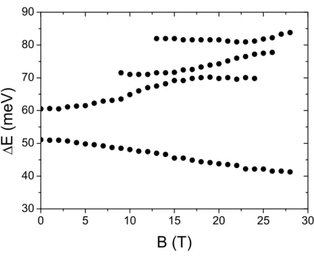
for Edet = 1215 meV. . . 89
4.8 Different exciton states classified by their z-direction angular momen-tum, Lz. . . 92
4.9 Schematic of the energy evolution in a magnetic field of the six non-interacting exciton-phonon states. . . 95 4.10 Diagram of the coupling interactions between the six exciton phonon
states of our calculation. . . 97 4.11 Calculated excitonic polaron energies and intensities as a function of
the magnetic field. The area of the circles is proportional to the oscil-lator strength of the transitions. The parameters for this calculation are given in Section 4.3. . . 99
4.13 Magnetic field dispersion of PLE resonances in sample P3 in open figures with the calculated energy transitions in solid lines (a) and a zoom (b) of the polaron states (1), (2), and (3), as labeled in Fig. 4.14. Parameters used in this calculation are given in the text. . . 102 4.14 Calculated excitonic polaron energies and intensities as a function of
the magnetic field (a) and a zoom (b) of the anticrossing between polaron states (1) and (2). The solid lines in (b) correspond to non-interacting exciton-phonon states. The area of the circles are propor-tional to the oscillator strengths. . . 103 4.15 Experimental (full squares) and calculated (solid lines) spectra for
different magnetic fields. The experimental data was taken for an Edet=1215 meV and for sample P3. The parameters used in the
calcu-lation are given in the text. . . 105 5.1 A schematic of the RPL process in a QD (a). Energy domains for a
PLE measurement with a fixed detection energy, Edet = 1215 meV and
for a RPL measurement with a fixed excitation energy, Eexc = 1293
meV (b). . . 110 5.2 Zero field comparison of an RPL spectrum (a) taken for a fixed Eexc
= 1293 meV and PLE spectrum (b) measured for a fixed Edet = 1215
meV. Both spectra were recorded on sample P3 at 4 K. . . 111 5.3 Magneto-RPL spectra recorded on sample P3 at 4 K from B = 0 to
28 T every 4 T and for Eexc = 1293 meV. Traces have been vertically
offset for clarity. The dashed lines are guides for the eyes. . . 113 5.4 Magneto-RPL spectra recorded on sample P3 at 4 K from B = 0 to
28 T every 4 T and for Eexc = 1260 meV. Traces have been vertically
offset for clarity. The dashed lines are guides for the eyes. . . 114 5.5 Schematic of the exciton energy levels displayed as a function of dot
parameters. The dashed arrows represent the relaxation process during a RPL measurement with Eexc = 1293 meV at B = 0 T (a) and when
a magnetic field is applied (b). . . 116 5.6 Schematic of the exciton energy levels displayed as a function of dot
parameters. The dashed arrows represent the relaxation process during a RPL measurement with Eexc = 1260 meV at B = 0 T (a) and when
a magnetic field is applied (b). . . 117 xv
N2 at 4 K from B = 0 to 28 T for Eexc = 1259 meV (b). Traces have
been vertically offset for clarity. The dashed lines are guides for the eyes.119 5.8 RPL spectra of sample P3 taken at 4 K for Eexc = 1260, 1273, 1287
and 1293 meV at 0T. . . 120 5.9 Magnetic field dispersion of RPL resonances for Eexc = 1293 meV (a)
and Eexc = 1260 meV (b) of sample P3 in symbols. The solid lines are
the polaron energy levels, calculated in Chapter 4, shifted to fit the RPL experimental results, as explained in the text. . . 122 5.10 Calculated excitonic polaron energies and intensities as a function of
the magnetic field. The area of the circles is proportional to the oscil-lator strength of the transitions. The parameters for this calculation are given in Section 4.3 of Chapter 4. . . 123 5.11 In dashed lines, the evolution of the detection energy and intraband
energy transition for QDs of fixed radius R = 115 ˚A and varying height. In solid line, the same evolution for dots of fixed height h = 28 ˚A and varying radius. Symbols are the experimental results obtained from RPL and PLE experiments, as described in the text. . . 125 5.12 Experimental (full symbols) and calculated (solid lines) spectra for
dif-ferent magnetic fields. The experimental data was taken for Eexc=1260
meV (a) and Eexc=1293 meV (b), for sample P3. The parameters used
in the calculation are given in the text. . . 126 5.13 All calculated polaron energies and intensities as a function of magnetic
field. No polaron level with significant OS is predicted in the vicinity of 110 meV. . . 128 5.14 Strain-modified valence band offsets calculated along the z-direction [9].
Both heavy hole states and a light hole state are found. Figure taken from reference [9]. . . 129 A.1 Band structure of bulk InAs and GaAs near the BZ center, including
the conduction band Γ6 and valence bands Γ7 and Γ8. . . 137
A.2 Schematic of QD energy levels. Each level has a corresponding envelope function and atomic part. . . 138 A.3 Schematic comparison between the magnetic field induced spin
split-ting energy, assuming a magnetic field of 28 T, and the FWHM of a PL peak. . . 139
Ep− Es. . . 140
1.1 Names and doping concentrations of samples presented in thesis. Sam-ples P1 and P2 were grown during the same MBE run. SamSam-ples U1, N2 and P3 were grown during the same MBE run. . . 13 1.2 Summary of different PL methods used in this thesis. . . 23
This thesis is a report on the carrier phonon interaction in semiconductor quantum dots. A quantum dot is a nanoscale object that, similar to an atom, presents the unique ability to confine electrons in the three dimensions of space. For this reason, quantum dots are commonly known as “artificial atoms.” Such systems are interesting as much for the study of their fundamental physical properties as for their possible device applications. Many applications of quantum dots have been predicted, such as single quantum dot transistors or quantum dot lasers [1, 2, 3, 4]. Keeping in mind these possible applications, the work presented in this thesis attempts to investigate and explain some of the fundamental physical properties of these nanostructures. In particular, the coupling between a carrier confined in a dot and the vibrations of the semiconductor lattice in which the quantum dot resides, is studied. Understanding this interaction mechanism is essential for the general understanding of the electronic properties of quantum dot systems. In essence, it is found that electronic and lat-tice excitations strongly mix to form the so-called polaron states of quantum dots. From the theoretical point of view, the quantum dot polaron state reflects a complex entanglement of electronic and phonon states. This study evidences the existence of polaron states in quantum dots, whether the confined carrier be an electron, hole or exciton.
Chapter 1
The first chapter will be dedicated to both the calculation of the discrete energy levels of a quantum dot structure, as well as to the experimental means of investigating these levels.
The InAs/GaAs quantum dot samples studied in this thesis were grown using the Stranski-Krastanov mode, which, in particular, exploits the lattice mismatch of the two materials to create nanoscale islands. The confining potential in a quantum dot structure, that induces the quantization of the carrier energy levels, depends on the size, shape, and composition of these islands. In addition, for dots grown using this mode, the strain, created as a result of the lattice mismatch between InAs and GaAs, also has a large influence on the confining potential. The calculation of the discrete energy levels of a quantum dot therefore depends on these, for the most part unknown and difficult to control, growth parameters. However, the essential ingredient of the dot potential is its ability to confine carriers in the three directions of space. The remaining parameters (strain, inhomogeneous InAs/GaAs content, piezoelectric effects) are secondary [5]. For this reason, a simple model, that takes the confining potential and effective mass of the carrier as adjustable parameters,
has been used to calculate the energy levels of a quantum dot system. The values of the parameters are chosen to obtain results in good agreement with the experimental results. The energy levels calculated in the first chapter will be of use throughout the thesis.
The intraband energy transitions of a carrier confined in a quantum dot can range from 20 meV for holes to 60 meV for electrons. Far infrared magnetospectroscopy is therefore employed to probe these energy levels. The magnetic field is an important experimental parameter, as it allows for the evolution of the energy levels, necessary for the observation of electronic and hole polaron levels.
The interband ground state energies of the quantum dot samples studied in this thesis are found in the mid infrared energy range. Magnetophotoluminescence exper-iments are therefore conducted to investigate the interband energy transitions and in turn the excitonic polaron energy levels.
Chapter 2
In Chapter 2, the polaron states of quantum dots systems will be calculated and their existence experimentally evidenced in n-doped samples.
In bulk, quantum well and quantum wire structures, the interaction between a charged carrier and longitudinal optical phonons allows for the rapid relaxation of an excited carrier to its ground state. In these cases, the relaxation process is well described by Fermi’s Golden rule. Longitudinal optical phonons play a very different role in quantum dot systems which, unlike the structures alluded to above, possess discrete electronic energy levels. Fermi’s Golden rule no longer applicable, it is found that the carrier and phonons in quantum dot structures are strongly coupled to one another. This coupling leads to the formation of polaron states, the true excitations of a charged dot. The calculation of these polaron states, presented in Chapter 2, will be used throughout the thesis as it can be applied to dots containing electrons, holes or excitons.
In order to verify the above polaron model, magnetotransmission results for n-doped samples reported in the thesis of J.N. Isaia [6] and S. Hameau [7] will be presented. In addition, new experimental results in magnet field using polarized light will be presented as complementary support of the polaron model, as applied to n-doped dots.
Chapter 3
Chapter 3 will be dedicated to the investigation of p-doped samples and the hole polaron state.
To date, there have been few investigations of the valence band magneto-optical transitions in quantum dots and therefore no direct evidence for the formation of hole magnetopolarons. The hole excitations of p-doped samples in polarization and in intense magnetic fields will be investigated here. The results will be interpreted using the polaron model for the case of a positively charged hole.
The differences between hole polaron states and their electron counterparts will be highlighted. In particular, as the intraband transitions energies of holes (∼ 20 meV) are found below that of electrons (∼ 60 meV), holes are found to primarily
interact with an InAs-like phonon mode, as compared to the GaAs-like phonon found in interaction with electrons.
Chapter 4
The understanding of the behavior of an electron-hole pair (exciton) confined in a quantum dot, is of utmost importance if these systems are to be used for application purposes (lasers, unique photon sources, . . . . ). Chapter 4 investigates such systems using the technique of photoluminescence excitation under strong magnetic fields.
Effects, such as the Coulomb interaction felt between the two carriers, differenti-ate the situation of an exciton trapped in a quantum dot from the case of a single charged particle. In addition, as the coupling between a carrier and optical phonons is basically electrical (Fr¨ohlich interaction), one could expect a rather small coupling be-tween phonons and the neutral exciton. The calculation presented in Chapter 4, will reveal that, in spite of their electrical neutrality, exciton and phonons are in a strong coupling regime and the formation of excitonic polaron states is indeed predicted. The simulated magnetoabsorption spectra will be compared to the experimentally obtained magnetophotoluminescence excitation spectra.
Chapter 5
The self-assembled InAs/GaAs samples investigated in this thesis contain not one unique quantum dot, but a large population of dots (dot density per layer∼ 1010cm−2).
In Chapter 5, the consequences that arise from the size inhomogeneity among dots of a single sample will be demonstrated through the study of resonant photoluminescence experiments in intense magnetic fields.
The photoluminescence peak of a quantum well structure can be homogeneously broadened due to, e.g., thermal spreading and slight non-uniformity of the interfaces. In self-assembled quantum dot samples, a large number of dots with different sizes, shapes and compositions and therefore electronic levels, are present. The inhomo-geneous broadening observed in the photoluminescence spectra of such samples is in part a consequence of the distribution of different dots in a single sample. The effect of this distribution on the behavior of resonant photoluminescence spectra will be studied.
Finally, these same results will be compared to the excitonic polaron energy level and oscillator strength calculations of Chapter 4.
[1] L. Guo, E. Leobandung and S.Y. Chou, A Silicon Single-Electron Transistor Memory Operating at Room Temperature, Science 275, 649 (1997).
[2] N. Kirstaedter, N.N. Ledentsov, M. Grundmann, D. Bimberg, V.M. Ustinov, S.S. Ruvimov, M.V. Maximov, P.S. Kop’ev, Zh.I. Alferov, U. Richter, P. Werner, U. G¨osele, and J. Heydenreich, Low threshold, large To injection laser emission from
(InGa)As quantum dots, Electronics Lett. 30, 1416 (1994).
[3] D. Bimberg, M. Grundmann, and N.D. Ledenstsov, Quantum Dot Heterostruc-tures, Wiley (1999).
[4] D. DiVencenzo, The Physical Implemtation of Quantum Computation, Fortschr. Phys. 48, 771 (2000).
[5] A. Vasanelli, Ph.D. thesis, Transitions optiques interbandes et intrabandes dans les boˆıtes quantiques simples et coupl´ees verticalement, Universit´e Paris VI (2002).
[6] J.N. Isaia, Ph.D. thesis, Niveaux ´electronique et interaction ´electron-phonons dans les boˆıtes quantiques d’InAs/GaAs, Universit´e Paris VI (2002).
[7] S. Hameau, Ph.D. thesis, Syst`emes d’´electrons dans les nanostructures semi-conductrices `a confinement quantique dans 2 ou 3 directions, Universit´e Paris VI (2000).
Presentation of Quantum Dots
In this chapter, a general presentation of quantum dots (QDs) and how they are investigated is given. First, a brief history of these systems along with the motivation behind their study is presented. Then a description of the fabrication of the QD samples used in this thesis is given. Finally, a description of how the energy levels of these systems are calculated is presented followed by the means of investigating these energy levels experimentally.
1.1
History and Motivation
As early as the 1950s, the idea of using ultra-thin layers of certain materials for the study of size quantification existed. This presumption became a working reality a few decades later with the development of new growth methods such as molecular beam epitaxy. In the early 1970s, the first low dimensional heterostructures, known as quantum wells (QWs), were developed. A heterostructure consists of a layered stack of semiconductors with different energy band gaps. The movement of electrons in one of these layers is restricted to only two dimensions. Such structures, that form the basis of most of the optoelectronic devices available today, were rather well understood by the end of the 1980s. This led physicists to investigate the possibility of further reducing the dimensionality to create 1D (quantum wire) and 0D (quantum dot) structures. Figure 1.1 shows schematically the evolution of the energy of an electron and the density of states as the dimensionality of the system is reduced. For QDs, the energy spectrum of an electron is discrete like in atomic physics, hence the adoption of the term “artificial atom.” The study of these artificial atoms has proven useful to explore a wide range of physical phenomena. Moreover, these nanostructures have a great potential for technological applications. Many applications in optoelectronics have been predicted, such as lasers, FIR detectors and quantum computing [1, 2, 3].
E1 E2 E3 x z y E kr E // kr E1 E2 D(E) E 3D
(bulk) (Quantum Well)2D
E x k E1 E2 E D(E) E1 E2 E D(E) E1 E2 1D
(Quantum Wire) (Quantum Dot) 0D
E
E D(E)
E1 E2 E3
(a) (b) (c) (d)
Figure 1.1: Evolution of the energy E of an electron and of the density of states as the dimensionality of the structure is reduced from 3D (bulk) (a) to 0D (quantum dot) (d).
1.2
Fabrication
One popular and practical method to grow QDs is the Stranski-Krastanov (SK) growth mode. This growth process, which consists in utilizing the lattice mismatch between two semiconductor materials to create nanometer-scale islands that can trap carriers, was first proposed by I.N. Stranski and L. Krastanov in 1937. All the sam-ples used in this work (InAs QDs in GaAs) were grown using the SK method. Using molecular beam epitaxy (MBE), InAs is deposited on a GaAs substrate. The lattice mismatch between the two materials (7%∗) introduces strain. The first few layers of
InAs form a 2D layer which is called the wetting layer (WL) [Fig. 1.2(a)]. After a critical thickness is reached, there is a relaxation of the strain and 3D growth becomes energetically favorable. Subsequently, small islands of InAs are spontaneously formed on the WL [Fig. 1.2(b)] [4]. This transition from 2D to 3D growth, called the SK Transition, occurs in InAs/GaAs systems for a critical thickness of 1.7 to 1.8 mono-layers [5]. The islands that form as a result of this transition are called self-organized or self-assembled quantum dots. The island structures are then covered with a GaAs epitaxial layer [Fig. 1.2(c)]. A 3D array of QDs can then be created by repeating the growth process described above. If the distance between successive InAs layers is less than 20-30 nm (depending on the dot size) , the QDs in successive layers tend to be aligned in order to minimize the elastic strain energy of the InAs layers. For thicker GaAs spacer layers, no vertical coupling is observed [6]. The size and den-sity of the islands strongly depend on the growth parameters: temperature during growth, growth rate, thickness of the epitaxy layers [7, 8]. The typical dimensions of QD islands range from 12 to 25 nm laterally and from 2 to 5 nm in height. An InAs island therefore is made up of about 104 atoms. The size dispersion of the dots
in a given sample can range from 10 to 15%. The average density of dots per layer can range between 108 and 1011 cm−2 [9]. Images taken using AFM (atomic force
microscopy) help one to visualize the form and organization of the islands in a layer, as shown in Fig. 1.3.
10 Chapter 1. Presentation of Quantum Dots
(c)
(a)
(b)
Stranski-Krastanov Transition GaAs substrate InAs <1.7 monolayers GaAs substrate InAs >1.7 monolayersFigure 1.2: Different stages of the SK growth process of InAs dots on a GaAs sub-strate.
Figure 1.3: AFM image of a layer of InAs/GaAs self-assembled quantum dots (J.M. Moison CNET-Bagneux).
InAs
wetting layer
20nm
InAs dot
about 2nm
Substrate
GaAs
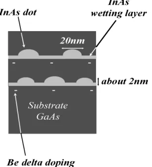
- --Be delta doping
- --Figure 1.4: Representation of the placement of Be layers 2 nm under each dot layer (δ-doping).
1.3
Characteristics of Samples
The samples investigated in this thesis were made at the Laboratoire de Photonique et Nanostructures by Aristide Lemaˆıtre. Samples containing a multistack of 20 layers of InAs QDs were prepared using MBE. The presence of a multistack of layers, as a opposed to a single layer, is necessary when conducting far infrared (FIR) absorption measurements as a resonant absorption associated with a single dot layer is weak (a few 0.1%) [10]. It is therefore important to point out that we present a study of QD ensembles and not single dots. This has for consequence, for example, the broadening of a PL peak due to size dispersion of the dots in a sample.† However, as each dot
layer is separated by a 50-nm-thick GaAs barrier and has a density of dots per layer of ∼ 4 × 1010 cm−2 (interdot distance of ∼ 50 nm), no coupling between dots is
expected and the QDs can be considered as isolated [6]. Cross sectional transmission electron spectroscopy in samples grown in similar conditions have shown that the QDs resemble flat truncated cones with an ∼ 20 nm basis diameter and an ∼ 3 nm height [11]. This thesis presents experiments performed on n-doped, p-doped and undoped samples. For the n-doped (p-doped) samples the dot filling was realized by a Si (Be) δ-doping of each GaAs barrier at 2 nm under each dot layer (see Fig. 1.4). The doping concentration was adjusted to transfer on average one to two carriers per dot. The characteristics of each sample used in this work is presented in Table 1.1.
Sample Name δ-doping Doping concentration (cm−2) N1 Si 6· 1010 P1 Be 5· 1010 P2 Be 10· 1010 U1 undoped -N2 Si 4· 1010 P3 Be 4· 1010
Table 1.1: Names and doping concentrations of samples presented in thesis. Samples P1 and P2 were grown during the same MBE run. Samples U1, N2 and P3 were grown during the same MBE run.
GaAs
InAs WL
E
CB
VB
InAs QD
Figure 1.5: Schematic of conduction band (CB) and valence band (VB) states of an InAs/GaAs system: 3D continuum states of the GaAs substrate in black, 2D continuum states of the InAs WL in grey and the discrete energy levels of the InAs QD in solid lines.
1.4
Electronic States
1.4.1
Electronic Structure of an InAs/GaAs System
A sample of InAs/GaAs self-assembled QDs possesses three different kinds of elec-tronic states: the 3D continuum states of the thick GaAs layers, the 2D continuum states of the InAs WL, and finally the 0D discrete states of the InAs QD. Figure 1.5 represents schematically the density of states of the conduction and valence bands of an InAs/GaAs structure.
In order to calculate the energy levels in QDs, one needs to consider the size, shape and composition of the dot, as well as the strain effects. This is a difficult task since all these parameters can not be controlled during the growth process and most of the time are not known with great precision. Different methods have been proposed to model QDs: the 8-band k·p method [12], the empirical pseudo-potential method [13], the tight binding method [14], the effective mass method [15]. We have chosen a one band (parabolic) effective mass method to calculate the QD energy levels. The results found using this method are consistent with those obtained using the more complex methods mentioned above [16]. Such a model also gives an accurate description of the coupling between electrons and phonon modes in n-doped samples [17, 18].
h
R
30°
z
Figure 1.6: Truncated cone of height h and radius R used to model the QD. The z-axis is the growth direction of the sample.
a simple model is less evident for the valence levels of semiconductor nanostructures, as discussed in many works (see e.g. Ref. [12] and [19] and references there in). For instance, non-parabolicity and mass anisotropy should play an important role in the description of the hole states. In order to account for these effects in a simplified and efficient way, we consider an anisotropic dispersion for heavy holes, with an in-plane mass chosen to best fit the experimental results. The light hole is left out of our calculations as its confinement energy is close to the top of the GaAs valence band [15, 16].‡ This model suffices to provide a good description of our experimental
results using reasonable fitting parameters [20].
1.4.2
Calculation of Energy Levels
Here we will summarize the calculation developed in the thesis of O. Verzelen [21]. In order to calculate the energy levels of a carrier (hole or electron) in a QD, the shape of the dot is modeled by a truncated cone of height h and with a circular basis of radius R and basis angle of 30◦, as shown in Fig. 1.6. Using the envelope function
approximation, the wave function of a carrier in such a dot can be described by the product of a Bloch function and a function that varies slowly (called the envelope function) over a distance on the scale of an elementary unit cell of the lattice. The Hamiltonian for the envelope function is written:
H = Ez+ Eρ,θ+ V(ρ, z), (1.1)
where Ez and Eρ,θ are the z-direction (growth direction) and in-plane kinetic energies
respectively and V(ρ, z) corresponds to the confinement potential that is equal to 0 outside the dot and −V0 inside the dot. V0e (V0h) is defined as the conduction
(valence) band offset between InAs and GaAs. The band gap of strained (due to the
surrounding GaAs) InAs is ∼ 0.53 eV at T = 4 K as compared to 0.41 eV for bulk InAs at the same temperature [22]. For pure InAs islands, taking into account that the energy band gap of GaAs at 4 K is 1.52 eV, Ve
0 = 572 meV for an electron and V0h
= 418 meV for a hole [23]. During the growth process, GaAs interfuses into the QDs so that the islands are not pure InAs, but contain a certain percentage (∼ 30 − 50%) of GaAs [24]. The conduction and valence band offsets depend on this percentage, which in turn depends on the growth parameters. As the growth parameters can change from sample to sample, we choose the interdiffusion percentage (and therefore offsets) to best fit the data of a sample.
Given that the confinement potential has a cylindrical symmetry, the eigenstates of the QD system are also eigenstates of Lz, the projection of the angular momentum
in the z-direction. Using the same nomenclature as in atomic physics the QD states can be denoted as follows:
Lz = 0 ↔ |si, ground state
Lz =±1 ↔ |pi, first excited state
Lz =±2 ↔ |di, second excited state
. . . ↔ . . . .
The ground state possesses an s-like symmetry and therefore has a wavefunction that is independent of θ. The first excited state is p-like and has a 2-fold degeneracy.§ The
number of excited states in the dot depends on its size.
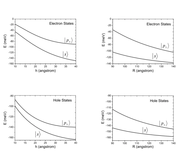
To calculate the s and p states of the system, a variational method has been employed [21]. Gaussian functions that respect the symmetry of the s and p states are taken as trial wavefunctions:
ψs(~r) = ψs(ρ, θ, z) = 1 pσsβs2π3/2 exp µ − ρ 2 2β2 s − (z− z0s) 2 2σ2 s ¶ (1.2) ψp±(~r) = ψp(ρ, θ, z) = ρ q σpβp4π3/2 exp µ − ρ 2 2β2 p − (z− z0p) 2 2σ2 p ± iθ ¶ (1.3) For each wavefunction we have three adjustable parameters: β the in-plane width of the wavefunction, σ the z-direction width, and z0 the center of the gaussian along
the z-axis. By minimizing the energy associated with these functions, the energy eigenvalues of the s and p states can be found. In Fig. 1.7, these energies are presented as a function of the height h of the QD and its radius R. An in-plane electron (heavy hole) mass of me = 0.07mo (mh = 0.22mo) was used in this calculation as well as a
conduction (valence) band offset of Ve
0 = 290 meV (V0h = 212 meV) which corresponds
to an average homogeneous gallium content of ∼ 50%.
We find that the height has more of an influence on the confinement of the carrier in the dot, whereas the radius more affects the intraband energy differences (Ep−Es).
For a dot size typical of our samples, i.e. R = 115 ˚A, h = 28 ˚A, an s− p intraband energy difference of 47 meV for electrons and 19 meV for holes is found.
10 15 20 25 30 35 40 -160 -140 -120 -100 -80 -60 -40 -20 0 p s E ( m e V ) h (angstrom) Electron States 90 100 110 120 130 140 -140 -120 -100 -80 -60 -40 -20 0 Electron States p s E ( m e V ) R (angstrom) 10 15 20 25 30 35 40 -160 -140 -120 -100 -80 p s E ( m e V ) h (angstrom) Hole States 90 100 110 120 130 140 -160 -150 -140 -130 -120 -110 -100 -90 Hole States p s E ( m e V ) R (angstrom)
Figure 1.7: The energies of the s and p states for an electron (top) and a hole (bottom) confined in a quantum dot as a function of the height h of the dot (left, with a fixed radius R = 115 ˚A) and as a function of the radius R (right, with a fixed height h = 28 ˚
A). The zero energy is taken at the bottom of the GaAs conduction for the electrons and the top of the GaAs valence band for the holes.
Anisotropy of Dots
In the above model, a 2-fold degeneracy is found in the p states. Experimentally, we find that this degeneracy is lifted. This is due to the fact that self-assembled quantum dots display a slight in-plane anisotropy, along the [110] and [1¯10] directions of the sample. Different effects have been considered in literature to explain this anisotropy. In the pseudopotential model this anisotropy arises from the C2v atomistic symmetry
of zinc blende crystals which distinguishes between these two directions [19]. In the framework of the one-band envelope function formalism the anisotropy has been attributed to the phenomenological shape anisotropy of the dots [10, 25]. In any case, the main effect of the anisotropy is to split the two degenerate lz =±1 levels of
the QDs. The splitting of the two levels at B = 0 T is clearly observed in the FIR absorption spectra of doped dots, as seen in Figure 1.8. The absorptions correspond to the intraband transitions between the s and p states. The spectra for light linearly polarized along the [110] and [1¯10] directions of sample N1 [Fig. 1.8(a)] and P1 sample [Fig. 1.8(b)] are presented. The anisotropy related energy splitting is found to be ∼ 10 meV for the n-doped sample and ∼ 1 meV for the p-doped. To account for this splitting in our cylindrical basis, we have treated the in-plane anisotropy in perturbation by introducing a coupling term, Va, whose matrix element, between the
p+ and p− states, is equal to half of the observed splitting:
2hp+
e|Vea|p−ei = 2δae = 10 meV
80 70 60 50 40 5% (a) T r a n s m i s s i o n Energy (meV) 30 28 26 24 22 20 (b) 2% Energy (meV)
Figure 1.8: FIR transmission spectra at B = 0 T for radiation linearly polarized along the [110] (solid curve) and the [110] (dashed curve) directions for sample N1 (a) and sample P1 (b). The observed absorptions correspond to the s-p intraband transitions. The curves in (a) have been vertically offset for clarity.
1.5
Investigation of Energy Levels
In order to investigate the energy levels of a carrier in a QD, the system needs to be excited. As shown in the preceding section, the intraband energy differences of holes (electrons) are ∼ 20 meV (50 meV), which are found in the the far infrared energy range. A magnetic field is applied in order to further the investigation, as it can be used to tune the energy separation between different states in the dots. FIR magnetospectroscopy experiments have been performed to investigate the intraband energy transitions of the systems. In addition, magneto-photoluminescence experi-ments were conducted in order to study the interband transitions of the dots. In this section, a detailed description of these two experimental methods is given, followed by a discussion of the coupling between a charged carrier with light and a magnetic field.
1.5.1
FIR Magnetospectroscopy: Intraband Transitions
A schematic for the setup of a FIR magnetospectroscopy experiment is shown in Fig. 1.9. The light source is a mercury vapor lamp. The FIR light is directed through a Michelson interferometer, which consists of a mylar beamsplitter and two mirrors. The light first hits the beamsplitter where half the beam is reflected to a stationary mirror and the other half passes through to a moving mirror. When the two halves of the beam recombine again on the beamsplitter they exhibit a path length difference x due to the mobile mirror. The recombined beam leaves the interferometer and is directed into the cryostat through the sample and is finally focused on the detector. The detector measures the intensity Itr(x) of the combined FIR beams as a function
of the moving mirror displacement x, the so-called interferogram. Finally, the com-puter calculates the Fourier transform of the interferogram to obtain a transmittance spectrum, Itr(σ), where σ is the wavenumber [26].
A particular beamsplitter can have a thickness ranging from 3.5 to 12 µm. The 3.5 and 6 µm beamsplitters are both good candidates to use for investigating the intraband transitions for p- or n-doped samples, as they both possess good intensity spectrum in the range of 100-700 cm−1 (∼10-90 meV).
The experimental setup at ENS in Paris uses a superconducting magnet, found inside the cryostat, which can produce magnetic fields up to 17 T. For the FIR experi-ments conducted at the High Magnetic Field Laboratory in Grenoble, in collaboration with Marcin Sadowski and Marek Potemski, a resistive magnet, which can reach 28 T, is used.
The applied magnetic field, as well as the propagation direction of the light are parallel to the growth axis of the sample. The sample is placed in a cryostat in a liquid helium bath that is pumped to a temperature of 2 K. Finally, the detector is a Si-composite bolometer that works at liquid helium temperatures.
It is possible, in the experimental set-up in Paris, for a linear polarizer to be placed directly underneath the sample in the cryostat. The linear polarizer can be rotated to polarize the EM field in a certain direction in the plane perpendicular to the growth direction. In this way, we are able to measure the transmission spectra of different polarizations of light with an applied magnetic field.
detector:
Si-composite
bolometer
I
tr(x)
I
tr(σ)
x
beamsplitter
I
0(σ)
I
0(x)
Mercury
lamp
O
Moving
mirror
Fixed
mirror
magnet
sample
polarizer
Figure 1.9: Schematic of the experimental setup, found at ENS in Paris, which mea-sures the FIR transmission of a sample in polarized light and an applied magnetic field.
In order to obtain a transmission spectra containing only the features interesting to our study, we divide the transmission spectra of a sample by that of its substrate [T (σ) = Isample(σ)/Isubstrate(σ)]. The substrate is obtained by cutting a small
rectan-gle from the sample wafer and sanding off the QD layers until we are left with just the GaAs substrate. The sample and substrate are mounted to the end of a pivoting rod. The rod can be rotated from outside the cryostat and therefore two spectra, Isample(σ) and Isubstrate(σ), can be measured in the same conditions, i.e. temperature,
polarization, and incident light.
1.5.2
Magneto-Photoluminescence: Interband Transitions
During a photoluminescence (PL) experiment, electron-hole pairs are created by shin-ing a laser on a sample. In the case of our QD samples, the pairs are trapped in the InAs islands and will relax to the ground state of the system (se− sh). Finally, the
pair recombines by emitting a photon, which we are able to detect with either a photomultiplier or a CCD (charge coupled device) camera.
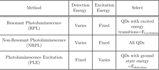
In this thesis, three different types of PL measurements are used: non-resonant photoluminescence (NRPL), resonant photoluminescence (RPL) and photolumines-cence excitation (PLE).
In both NRPL and RPL measurements, the excitation energy of the laser is fixed, while detection is possible in a certain energy range. For NRPL, the excitation energy is fixed to be superior or equal to the GaAs energy gap. Initially, electron hole pairs are created in the GaAs lattice which eventually relax down into the quantum dot states. In this way, we are assured the creation of an electron hole pair in all the dots. The resulting NRPL spectrum is therefore the sum of the contribution of all the dots. In the case of RPL, the excitation energy is lower than the GaAs gap and the InAs WL (see Fig. 1.5). As a result, electron hole pairs will only be created in QDs with discrete excited energy transitions that correspond to the given excitation energy.
Finally, unlike the two methods described above, in a PLE measurement the detection energy is fixed while the excitation energy is varied. The detection energy is chosen to correspond to the luminescence of certain dots in the sample. The excitation energy is then varied through a certain energy range. When an excitation energy coincides with an excited state transition in a QD, an electron hole pair is created. The pair relaxes to the ground state and finally the electron and hole recombine and emit a photon. A signal is detected, at the chosen fixed detection energy, each time the excitation energy corresponds to an excited state transition of a dot. PLE, therefore, measures a signal from a subensemble of dots in the sample whose ground state energy corresponds to the chosen detection energy. A summary of the three PL methods is presented in Table 1.2.
All the PL data presented in this thesis was collected at the High Magnetic Field Laboratory in Grenoble, in collaboration with Francis Teran and Marek Potemski. A schematic of the setup for a magneto-RPL or NRPL experiment is shown in Fig. 1.10. An Ar+ laser is used for non-resonant excitation and a Ti:sapphire laser for resonant excitation. A chopper coupled to a lock-in amplifier allows the elimination of any optical noise. A system of optical fibers is used for the sample excitation and the collection of the PL signal. The sample is immersed in a liquid helium bath which
is pumped to 4 K. A resistive magnet surrounds the cryostat such that a magnetic field up to 28 T can be applied along the sample growth axis. The emitted light from the sample is dispersed through a Jobin Yvon spectrometer and detected by a photomultiplier.
The PLE experiment has the same set-up described above but uses a Ti:sapphire laser and a CCD camera for the detection.
Method Detection Energy Excitation Energy Select Resonant Photoluminescence (RPL) Varies Fixed QDs with excited energy transitions=Eexcitation Non-Resonant Photoluminescence
(NRPL) Varies Fixed All QDs Photoluminescence Excitation
(PLE) Fixed Varies
QDs with ground state energy
=Edetection
Figure 1.10: Schematic of the experimental setup, found at the High Magnetic Field Laboratory in Grenoble, which measures the RPL or NRPL signal in a high magnetic field.
1.5.3
Coupling to Light
The processes of both FIR spectroscopy and photoluminescence involve the inter-action between electrons and light. It is therefore necessary to study the coupling between a charged carrier and an electromagnetic field in a QD.
In the general case, the Hamiltonian of an electron of charge −e in the presence of an electric or magnetic field is written:
H = 1 2m0
³
~p− e~A(~r, t)´2− eφ(~r, t) + V (~r) (1.5) where ~A is the potential vector and φ the electrostatic potential. V represents the potential of the crystal lattice. The Hamiltonian H = H0+ Hi can be written in the
the Coulomb gauge (~∇ · ~A = 0, φ=0) as follows: H0 = p2 2m∗; Hi =− e ~A· ~p m∗ + e2A2 2m∗ (1.6)
Neglecting the term in A2 and applying the electric dipole approximation the inter-action Hamiltonian becomes [27, 28]:
Hi = ~ε· ~p
eE
m∗ωsin ωt (1.7)
where E is the amplitude of the electric field, ~ε the polarization of the EM wave, and ω its angular frequency. This term of the Hamiltonian is responsible for the provocation of the inter and intraband transitions of electrons. Indeed, the transition probability of an electron initially in the state |φii being excited to a final state |φfi
is proportional to:
Pi→f ∝ |hφf|~ε · ~p|φii|2 (1.8)
The wavefunction of a carrier in a quantum dot can be separated into two parts: the envelope function times a plane wave, which we will label fl (with l = s or p), on
the one hand and the periodic part of the Bloch function un on the other, where n is
either the conduction or valence band. We therefore have the initial and final wave-functions: φf = flfunf and φi = fliuni. Expressing the wavefunctions as such, allows for the separation of the matrix element in Eq. 1.8 into two terms: one responsible for intraband transitions and one for interband transitions [29].
Intraband Transitions
We first examine the intraband term. This term is important when interpreting FIR measurements, where intraband transitions of a QD system are directly probed. The oscillator strength (OS) of these transitions is proportional to:
OSi→f ∝ |hfli|~ε · ~p|flfi|
2 (1.9)
We notice that only the envelope part of the wavefunction plays a role in the OS of intraband transitions. Since the initial and final Bloch states are identical for intraband transitions (ni = nf = conduction or valence band), and these functions
oscillate rapidly compared to the envelope functions, their contribution to the OS can be neglected [29].
As a result of the symmetry of the states, for an EM wave polarized in the xy plane, only transitions between states whose orbital angular momentum differ by one (∆l =±1) are permitted. For our QD systems, in which only the ground state |si is populated, we find two allowed optical transitions, |si ↔ |p+i and |si ↔ |p−i.
Interband Transitions
We now look at the interband term, important for interpreting PL results. The polarization selection rules depend on the Bloch function part of this term,
huni|~ε · ~p|unfi. We notice that the rules are the same as those of the bulk material. However, because of the broadening of the PL peak due to size inhomogeneity in self-assembled dot samples, our experiments are not sensitive to the effects of the above term.¶ We are therefore only concerned by the envelope function contribution:
OSi→f ∝ |hfli|flfi|
2 (1.10)
This term is non-zero only when the initial and final states have the same l. The allowed optical interband transitions are therefore of the type: s→ s, p → p . . .
1.5.4
Coupling to a Constant Magnetic Field
The applied magnetic field is an important parameter in our experiments. Here, we will study the effect of a constant magnetic field on the electronic states of a QD. We consider the situation of our experiments, i.e. a magnetic field B applied along the growth axis of the sample. The potential vector ~A can therefore be written in the Coulomb gauge:
~ A = 1
2(−By, Bx, 0) (1.11) In these conditions and neglecting the term in A2, Eq. 1.6 becomes
H = H0+
eB
2m∗Lz (1.12)
The presence of a magnetic field introduces a term in the Hamiltonian proportional to the z-component of the angular momentum; the Zeemen effect.
Let us now look at the effect this new term has on the quantum dot energy states calculated in the previous section; s and p. As mentioned before, due to the cylindrical symmetry of the confinement potential, these states are eigenstates of Lz. Therefore,
the magnetic field does not couple the states between themselves. On the other hand, the magnetic field will affect the energies of these states:
Es(B) = Es(0) Ep+(B) = Ep(0) + ¯heB 2m∗ Ep−(B) = Ep(0)− ¯ heB 2m∗ (1.13)
0 5 10 15 20 25 30 0 10 20 30 40 50 60 70 80 90 Electron p p s E ( m e V ) B (T) (a) 0 5 10 15 20 25 30 0 10 20 30 40 Hole p p s E ( m e V ) B (T) (b)
Figure 1.11: s and p state energies as a function of the B field, for an electron (a) of mass me = 0.07mo and a hole (b) of mass mh = 0.22mo, confined in a QD with R=
These equations suffice when dealing with small magnetic fields. However, for stronger magnetic fields (≈20 T), the term in A2 of Eq. 1.6 can no longer be neglected.
Taking this into account, we find the diamagnetic term: Hdia = e2A2 2m∗ = e2ρ2 8m∗B 2 (1.14)
The total effect of the magnetic field on the QD energy states is therefore the addition of a Zeeman term and a diamagnetic term:
Es(B) = Es(0) + e2β2 sB2 8m∗ Ep+(B) = Ep(0) + ¯heB 2m∗ + e2β2 pB2 4m∗ Ep−(B) = Ep(0)− ¯ heB 2m∗ + e2β2 pB2 4m∗ (1.15)
Figure 1.11 shows the evolution of the ground state, s, and two excited states, p+ and
p−, of an electron (a) and a hole (b) confined in a QD as a function of the magnetic
field. The zero energy is taken at the ground state energy at 0T, Es(0). The m∗s
in Eq. 1.15 are replaced by me for an electron and mh for a hole. In the calculation
leading up to Eq. 1.15, we considered an electron in the presence of an EM field. With a simple change of charge sign (−e → +e), this same calculation can be applied to a hole. As a result, for a hole, the p+ (l = +1) energy level decreases in energy
with the magnetic field while the p− (l = −1) energy level increases, contrary to the
case of an electron. The mass of a hole being heavier than that of an electron (mh =
0.22mo compared to me= 0.07mo), we find that the energy dispersion for an electron
in a magnetic field is greater than that of a hole. Indeed, as shown in Fig. 1.11, the higher energy branch increases by 36 meV in 30 T for an electron compared to a 10 meV energy increase for the same variation in magnetic field for a hole. For both carriers, the diamagnetic effect becomes apparent for intense magnetic fields.
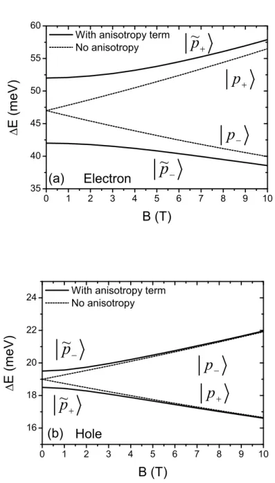
If we take into account the anisotropy discussed in the previous section, the p-state energies are now written:
Ep+(B) = Ep(0) + s µ ¯hωc 2 ¶2 + (δa)2+ e2β2 pB2 4m∗ Ep−(B) = Ep(0)− s µ ¯hωc 2 ¶2 + (δa)2+ e2β2 pB2 4m∗ (1.16)
with ωc= meB∗. These energies, for a hole and for an electron, are shown in Fig. 1.12. We find that the p+ and p− energy levels are no longer degenerate at 0 T, but are
separated by an energy equal to 2δa. The effect of the anisotropy on the p-states is
most noticeable for low magnetic fields. For more intense B fields, the p-states with anisotropy (in solid lines in Fig. 1.12) are very close to those without anisotropy (in dashed lines in Fig. 1.12). In what follows ˜p± will denote the two electronic levels
that result from the excited states admixed by the anisotropy term, i.e. the solid lines in Fig. 1.12.
0 1 2 3 4 5 6 7 8 9 10 35 40 45 50 55 60 p ~ p ~ Electron
W ith anisotropy term No anisotropy p p E ( m e V ) B (T) (a) 0 1 2 3 4 5 6 7 8 9 10 16 18 20 22 24 p p p ~ p ~
W ith anisotropy term No anisotropy E ( m e V ) B (T) Hole (b)
Figure 1.12: Energies of the p-states for an electron (a) and for a hole (b) as a function of magnetic field with anisotropy term included in the calculation (in solid lines) and without this term (dashed lines).The anisotropy term is 2δe
a = 10 meV for electrons
and 2δe
1.6
Conclusion
A general background of QDs was presented in this chapter. It was shown that, using the Stranski Krastanov growth mode, it is possible to grow samples containing an ensemble of QDs in which carriers can be confined in all three directions of space. All the samples studied in this thesis were fabricated using this method.
A presentation of the calculation of the confined states was then given, where we found that a carrier possesses discrete energy levels labeled by its z-direction angular momentum.
We have given a detailed description of the two experimental methods used to study these QD states. Far-infrared magnetospectroscopy and near-infrared magne-tophotoluminescence are employed to probe respectively the intraband and interband transitions of the system.
Finally, we have examined the interaction between a carrier trapped in a QD with light as well as with a magnetic field: situation which arises in the experiments. The QD intra and interband selection rules were established along with the evolution of the QD energy levels as a function of magnetic field.
Although we have found that QDs present many of the same attributes as atoms, we have already begun to discover the deficiency of the artificial atom model i.e. dots display an in-plane anisotropy. In the following chapters, we will further show that, because QDs are embedded in a semiconductor lattice, this simple image does not hold true. Indeed, the interaction between a charged carrier in a dot and its semiconductor environment, in particular the crystal lattice vibrations, differentiates dots from the isolated atom.
[1] N. Kirstaedter, N.N. Ledentsov, M. Grundmann, D. Bimberg, V.M. Ustinov, S.S. Ruvimov, M.V. Maximov, P.S. Kop’ev, Zh.I. Alferov, U. Richter, P. Werner, U. G¨osele, and J. Heydenreich, Low threshold, large To injection laser emission from
(InGa)As quantum dots, Electronics Lett. 30, 1416 (1994).
[2] Y. Arakawa and H. Sakaki, Multidimensional quantum well laser and temperature dependence of its threshold current, Appl. Phys. Lett. 40, 939 (1982).
[3] D. DiVencenzo, The Physical Implementation of Quantum Computation, Fortschr. Phys. 48, 771 (2000).
[4] L.Goldstein, F. Glas, J.Y. Marzin, M.N. Charasse, and G. Leroux, Growth by molecular beam epitaxy and characterization of InAs/GaAs strained-layer super-lattices, Appl. Phys. Lett. 47, 1099 (1985).
[5] J. M. G´erard, J. B. G´enin, J. Lefebvre, J. M. Moison, N. Lebouch´e and F. Barthe, Optical investigation of the self-organized growth of InAs/GaAs quantum boxes, J. Crystal Growth 150, 351 (1995).
[6] B. Legrand, J.P. Nys, B. Grandidier, D. Sti´evenard, A. Lemaˆıtre, J.M. G´erard, and V. Thierry-Mieg, Quantum box size effect on vertical self-alignment studied using cross-sectional scanning tunneling microscopy, Appl. Phys. Lett. 74, 2608, (1999).
[7] G. S. Solomon, J. A. Trezza, and J. S. Harris, Effects of monolayer coverage, flux ratio, and growth rate on the island density of InAs islands on GaAs, Appl. Phys. Lett. 66, 3161 (1995).
[8] G. S. Solomon, J. A. Trezza, and J. S. Harris, Substrate temperature and mono-layer coverage effects on epitaxial ordering of InAs and InGaAs islands on GaAs, Appl. Phys. Lett. 66, 991(1995).
[9] J. M. Moison, F. Houzay, F. Barthe, L. Leprince, E. Andr´e, and O. Vatel, Self-organized growth of regular nanometer-scale InAs dots on GaAs, Appl. Phys. Lett. 64, 196 (1994).
[10] M. Fricke, A. Lorke, J.P. Kotthaus, G. Medeiros-Ribeiro, and P.M. Petroff, Shell structure and electron-electron interaction in self-assembled InAs quantum dots, Europhys. Lett. 36, 197 (1996).
[11] B. Grandidier, Y. M. Niquet, B. Legrand, J. P. Nys, C. Priester, D. Sti´evenard, J. M. G´erard and V. Thierry-Mieg, Imaging the Wave-Function Amplitudes in Cleaved Semiconductor Quantum Boxes, Phys. Rev. Lett., 85, 1068 (2000). [12] O. Stier, Electronic and Optical Properties of Quantum Dots and Wires,
Wis-senschaft und Technik Verlag, (2001).
[13] L.-W. Wang, J. Kim, and A. Zunger, Electronic structures of [110]-faceted self-assembled pyramidal InAs/GaAs quantum dots, Phys. Rev. B 59, 5678 (1999). [14] S. Lee, L. J¨onsson, J.W. Wilkins, G.W. Bryant, and G. Klimeck, Electron-hole
correlations in semiconductor quantum dots with tight-binding wave functions Phys. Rev. B 63, 195318 (2001).
[15] J.-Y. Marzin and G. Bastard, Calculation of the energy levels in InAs/GaAs Quantum Dots, Solid State Commun. 92 437, (1994).
[16] A. Vasanelli, Ph.D. thesis, Transitions optiques interbandes et intrabandes dans les boˆıtes quantiques simples et coupl´ees verticalement, Universit´e Paris VI (2002).
[17] S. Hameau, J.N. Isaia, Y. Guldner, E. Deleporte, O. Verzelen, R. Ferreira, G. Bastard, J. Zeman, and J.M. G´erard, Far-infrared magnetospectroscopy of po-laron states in self-assembled InAs/GaAs quantum dots, Phys. Rev. B 65, 085316 (2002).
[18] S. Hameau, Y. Guldner, O. Verzelen, R. Ferreira, G. Bastard, J. Zeman, A. Lemaˆıtre, and J.M. G´erard, Strong Electron-Phonon Coupling Regime in Quan-tum Dots: Evidence for Everlasting Resonant Polarons, Phys. Rev. Lett. 83, 4152 (1999).
[19] G. Bester, S. Nair, and A. Zunger, Pseudopotential calculation of the excitonic fine structure of million-atom self-assembled In1−xGaxAs/GaAs quantum dots,
Phys. Rev. B 67, 161306 (2003).
[20] V. Preisler, R. Ferreira, S. Hameau, L. A. de Vaulchier, Y. Guldner, M. L. Sadowski, and A. Lemaˆıtre, Hole-LO phonon interaction in InAs/GaAs quantum dots, Phys. Rev. B 72, 115309 (2005).
[21] O. Verzelen, Ph.D. thesis, Interaction ´electron-phonon LO dans les boˆıtes quan-tiques d’InAs/GaAs, Universit´e Paris VI (2002).
[22] M. Levinshtein, S. Rumyantsev, and M. Shur, ed., Semiconductor Parameters: Volume 1, World Scientific (1996).
[23] J.N. Isaia, Ph.D. thesis, Niveaux ´electronique et interaction ´electron-phonons dans les boˆıtes quantiques d’InAs/GaAs, Universit´e Paris VI (2002).
[24] P. B. Joyce, T. J. Krzyzewski, G. R. Bell, B. A. Joyce, and T. S. Jones, Com-position of InAs quantum dots on GaAs(001): Direct evidence for (In,Ga)As alloying, Phys. Rev. B 58, R15981 (1998).
[25] Y. Hasegawa, H. Kiyama, Q.K. Xue, and T. Sakurai, Atomic structure of faceted planes of three-dimensional InAs islands on GaAs(001) studied by scanning tun-neling microscope, Appl. Phys. Lett. 72, 2265 (1998).
[26] R.J. Bell, Introduction to Fourier Transform Spectroscopy, Academic Press (1972).
[27] C. Cohen-Tannoudji, B. Diu, and F. Lalo¨e, M´ecanique Quantique, Hermann (1973).
[28] P. Yu, and M. Cardona, Fundamentals of Semiconductors, Springer-Verlag (1999).
[29] G. Bastard, Wave mechanics applied to semiconductor heterostructures, Les Edi-tions de Physique (1996).

![Figure 1.8: FIR transmission spectra at B = 0 T for radiation linearly polarized along the [110] (solid curve) and the [110] (dashed curve) directions for sample N1 (a) and sample P1 (b)](https://thumb-eu.123doks.com/thumbv2/123doknet/2325597.30264/40.892.164.755.314.799/figure-transmission-spectra-radiation-linearly-polarized-dashed-directions.webp)

![Figure 2.1: Phonon dispersion curve in GaAs along the high symmetry axis Γ −∆−X found in reference [15].](https://thumb-eu.123doks.com/thumbv2/123doknet/2325597.30264/58.892.220.684.170.500/figure-phonon-dispersion-curve-gaas-high-symmetry-reference.webp)
![Figure 2.8: Calculated magnetic field dependence of the oscillator strength for the high energy polaron (solid lines) and the low energy polaron (dashed lines) for light polarized along the [110] (full circles) and [110](open circles) directions.](https://thumb-eu.123doks.com/thumbv2/123doknet/2325597.30264/69.892.178.709.459.869/figure-calculated-magnetic-dependence-oscillator-strength-polarized-directions.webp)