To link to this article:
DOI:10.1002/adem.201700109
URL :
http://dx.doi.org/10.1002/adem.201700109
This is an author-deposited version published in:
http://oatao.univ-toulouse.fr/
Eprints ID:
18272
To cite this version
:
Msolli, Sabeur and Alexis, Joël and Kim, Heungsoo Mechanical behavior
and adhesion of the Ti/Cr/Au metallization scheme on diamond substrate.
(2017) Advanced Engineering Materials, vol. 19 (n° 8). ISSN 1438-1656
O
pen
A
rchive
T
oulouse
A
rchive
O
uverte (
OATAO
)
OATAO is an open access repository that collects the work of Toulouse researchers and
makes it freely available over the web where possible.
Any correspondence concerning this service should be sent to the repository
administrator:
[email protected]
Mechanical Behavior and Adhesion of the Ti/Cr/Au
Metallization Scheme on Diamond Substrate
Sabeur Msolli, Joel Alexis, and Heungsoo Kim*
The mechanical properties of a Ti/Cr/Au metallization system deposited on a heavily doped diamond substrate are evaluated, first using nano-indentation tests. Various kinds of conditions are adopted, such as small and high force loadings. These tests are completed by in situ scanning electron microscopy observations of the surface. The adhesion of such multilayer on the diamond substrate is assessed using nano-scratching tests. The profiles of the obtained scratches are analyzed to detect any singularities or defects. Finally, a cross-section topography is performed, in order to obtain the cross profile of the scratch, and to determine the scratch hardness parameter of the metallization system. The Ti/Cr/Au metallization system is a potential candidate to play the role of ohmic contact on diamond. Therefore, its adhesion to diamond is important, since the whole power electronic assembly is mainly subjected to thermal cycling during service. The metallization system must adhere well to diamond, so as to resist temperature gradients and thermal strains that are widely observed in extreme thermal conditions. Otherwise, debonding phenomena may occur, and the whole electronic packaging fail.
1. Introduction
Nowadays, power electronics modules are mainly used as converters or inverters in aircraft-embedded electronic systems. The power module is presented as a composition of “active” components, such as semi-conductors and ohmic diodes mounted on one or many holders or substrates. Recent technologies use silicon and silicon carbide as constitutive materials for these active components. These materials are suitable in electronic applications, thanks to their mechanical properties and resistance at high temperature. The state-of-the-art indicates that an emerging generation of new power electronics modules are under investigation. The relevant modules are based on diamond ohmic diodes that can withstand higher power and temperatures of up to 300!C. The choice of the
metallization system to be deposited on the diamond chip is complex.[1]The metalliza-tion scheme must also withstand what a diamond die can endure. Several metalli-zation schemes deposited on diamond substrates were studied, from either the electrical, or the mechanical viewpoints. Thereby, Meyyappan et al. considered Au/ (Ti-W) and Au/Cr metallizations of CVD diamond substrates.[2] In their findings, out-diffusion of W through Au is observed at 400!C, but no interdiffusion in the case
of Au/Cr. There was also interaction between the metals in both Au/(Ti-W) and Au/Cr metallizations at 450!C. John-ston et al. showed that the preferred metallization scheme for ohmic contacts to CVD diamond for use in extreme conditions is Mo/Pt/Au, where Mo acts as the ohmic contact to the CVD diamond layer, after a suitable annealing step to form MoC.[3] Iaconvagelo studied Ti/Pt/Au, W-Ti/Au, and Nb/Au metallization systems on diamond substrate.[4]These metalliza-tions present excellent adhesion to dia-mond substrate. Among the metallizations, W-Ti/Au metallization system had the best performance. Tjong et al. compared some metallization schemes deposited on diamond substrate.[5–7]Scratch tests indicate the adhesion strength of NiTi films to the diamond substrate is slightly higher that of Cu, due to the formation of TiC. However, they show that only Cr is inert to AuSn solder during annealing. Zhen et al. compared Au and Au/Ta contacts fabricated on B-doped diamond films.[8] Compared with Au contact, Au/Ta contact has better adhesion. In addition, Au/Ta contacts have better ohmic characteristics, thanks to the presence of TaC. Hoff et al. studied the electrical performance of a Ti/Pt/Au trilayer scheme deposited on diamond substrate by an 800 and 900!C anneal in vacuum.[9] The paper concludes on the effectiveness of the Pt layer as a diffusion barrier to Ti, and the incidence on the electrical resistance. Katz et al. found that Ti/W/W(Ni3Sn4)/Ni3Sn4/Au multilayered structure was a suitable metallurgical scheme for the purpose of bonding laser chip to CVD-diamond sub-mount.[10,11]The authors also studied a Ti/Pt/Au-Sn metalliza-tion scheme for bonding of InP-based laser diodes to CVD diamond submounts. A high quality bond is obtained. Electrical performance of such metallization system was also assessed for use as ohmic contact on diamond.[12,13]More recently, Msolli et al. studied two kinds of metallization schemes, Ti/Pt/Au and Si/Al.[14]In contrast to the Si/Al metallization scheme, that is, Prof. H. S. Kim, Prof. S. Msolli
Department of Mechanical, Robotics and Energy Engineering, Dongguk University-Seoul, 30 Pildong-ro 1-gil, Jung-gu, Seoul 04620, Republic of Korea
E-mail: [email protected] Prof. J. Alexis
Universit!e de Toulouse; INP/ENIT; LGP; 47, Avenue d’Azereix; F-65013 Tarbes, France
suitable to be used in conjunction with Al based solders, the Ti/ Pt/Au metallization scheme is dedicated for use with assemblies brazed using AuGe solder alloy.[15]Nevertheless, this metalliza-tion presented several defects, including blisters on the surface, and chips on the edges of the produced scratches.
An alternative to this metallization system has to be proposed. The choice of the metallization must obey many rules, among which: (i) the metallization entities must be compatible with the used solder alloy to avoid the formation of fragile intermetallic compounds (IMCs), (ii) it must present an efficient diffusion barrier to avoid diffusion of solder entities into underlying layers, and (iii) it must have good mechanical and adhesion properties. Since germanium present in AuGe alloy is first responsible for the formation of IMCs, the choice of the diffusion barrier must be carefully performed. Nickel is widely used as a diffusion barrier in electronics microdevices. However, Ni forms brittle IMCs that may manifest even at room temperature. Interest is then focused on chromium as a potential diffusion barrier, since it has proved its usefulness in assemblies involving AuSn alloy. Noble metals are rather suited to oxidation barriers. Gold presents the most affinity with gold-based alloys, as the formation of IMCs is prevented. Titanium is chosen as an attachment layer to diamond, as together they form a strong carbide interphase layer, see for example.[16] In addition, the elaboration process is well controlled and understood.
The scope of this paper is the proposal of a new Ti/Cr/Au metallization system deposited on diamond to be applied as an ohmic contact, and to hold gold-based alloys, especially AuGe alloy. The study of the mechanical properties and the adhesion of the metallization system is performed. This study permits the assessment of the mechanical usefulness of the Ti/Cr/Au metallization system as a diamond metallization. The new trilayer should be suitable for use as an ohmic contact of diamond substrates. It presents an alternative to the Ti/Pt/Au
metallization scheme, and is compatible with gold-based eutectic alloys, such as AuSn and AuGe. The relevant metallization scheme is characterized experimentally using nano-indentation tests to evaluate the mechanical properties, and nano-scratching tests to assess the adhesion of the multilayer on the diamond substrate. The surface of the whole sample is analyzed to detect singularities or defects issuing from the deposition process. Finally, the morphology of the indents and the scratches are observed, to determine the presence of cracks or damages issuing from the imposed loading.
Experimental Section
The Ti/Cr/Au metallization system was deposited on 3" 3 " 0.5 mm lb diamond sample by vacuum evaporation. The Ti/Cr/Au multilayer was formed by a lift-off process. The thicknesses of the Ti, Cr, and Au layers were 0.03, 0.03, and 0.5 mm, respectively. The lift-off was followed by an annealing operation at 450!C for 30 min. Figure 1 shows a schematic of the layer stack. Once the specimen was elaborated, the elastic properties of the metallization system were determined at room temperature (23!C), by using an MTS©nano-indentation device equipped with a Berkovich
pyramidal indenter. For large and small displacements, the tests were performed with an MTS XP and a DCM tip, respectively. The adhesion of the deposited multilayers was also assessed using nano-scratching tests. The test parameters were adapted to the thickness of the metallization layer. Nano-scratching tests were performed on the sample surface by moving a Berkovich tip in three successive steps, and measuring the penetration depth. In order to assess the quality of the deposited metallization scheme, observations of sample surface, indents, and scratches were carried out by field emission gun scanning electron microscopy (FEG SEM-7000F from JEOL, with the incident electron beam maintained between 10 and 15 kV). SDD Bruker X flash energy dispersive X-ray spectrometry (EDX) was used for the chemical analysis of the constitutive species. See, for example, ref.[14] or ref.[17] for more details about the experimental procedure.
3. Results and Discussion
3.1. Morphology of the Ti/Cr/Au Metallization System
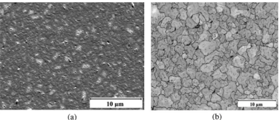
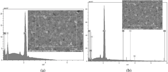
Figure 2a shows a micrograph of the morphology of the deposit that was obtained by Scanning Electron Microscopy (SEM). The structure of the surface is homogeneous, and free of any irregularities (Figure 2a). Using the back-scattered electrons mode, grains look equiaxed with a size of between 0.5 and 3 mm (Figure 2b). They are uniformly distributed on the surface of the deposit. Grains boundaries are clearly revealed. They also look distinct and complete, where all of the grain boundaries have etched equally well. Figure 3 shows the morphology of the deposit and the diffraction spectra. Based on the micrograph performed at higher magnification of"3500 and shown below, EDX spectroscopy reveals the presence of Au that covers all the surface of the metallization. Figure 3a shows that he EDX elemental analysis performed with moderate High Voltage (HT¼ 5.0 kV) reveals that Au is exclusively detected on the EDX spectrum. For Figure 1. Shematic representation of the layer stack deposited on the
diamond substrate, and the thickness of each deposited layer.
Figure 2. Micrograph of the surface of Ti/Cr/Au metallization system performed on diamond substrate. (a) Overall morphology of the sample surface, and (b) observation of the distribution of Au grains on the surface using back-scattered electrons mode.
higher HT values (HT¼ 10.0 kV), the whole set of deposition materials is detected. Figure 3b shows that the strongest peak is due to Au, which is the major component, since it has higher thickness. The spectrum of Figure 3b shows that Ti and Cr are present in minor proportions, due to the thinness of their deposited layers.
3.2. Mechanical Properties of the Ti/Cr/Au Metallization System
3.2.1. Nano-Indentation with MTS XP Indenter
Nano-indentation tests were performed by MTS XP indenter, which is dedicated to large nano-indentation depths. Figure 4 shows that the nano-indention tests performed on the metallized diamond substrate were all reproducible, as these kinds of tests are quite precise. The curves are continuous and smooth, as no damage or fracture was initiated in the diamond substrate or the
metallization system. A significant increase of the load was observed when the tip reaches the Cr layer (500 nm). Indeed, Figure 4 shows that once the tip reaches the Cr layer, the value of the applied force drastically increases, until reaching its maximal value of 700 mN. At this level, the nano-indentation response is becoming more sensitive to the diamond stiffness. Conversely, the unloading level is characterized by an important elastic recovery of 500 nm, as the elastic behavior of diamond is becoming predominant. Regarding the entire range of penetration depth, this elastic recovery is quite consequent, as the indented diamond is highly stiff, and negligible plasticity is recovered for the involved constitutive materials of the layer stack.
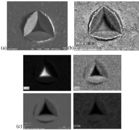
Figure 5a shows a micrograph of one of the indents issuing from the nano-indentation tests. Following this figure, no edge, radial cracks, or defects are detected, either in the subsequent layers, or in the diamond substrate itself. An important pile-up is observed at the edges of the indents. Chemical analysis using EDX spectroscopy did not permit detection of the chromium layer due to its thinness. Figure 5b shows the different results of this analysis in the EDX map. This map demonstrates that the important pile-up is mainly formed due to the plastic deformation of the gold layer. Regarding this map, the Cr layer is hardly detected, as it is very thin. Nevertheless, the indentation of the underlying Ti and C layers is apparent. Figure 5c shows a more detailed analysis of the chemical composition of the indent, and the presence of C, Ti, Cr, and Au by elemental mapping taken with energy dispersive X-ray (EDX). Figure 6 shows the EDX elemental spectrum of the indent. Au is mostly present at the contour of the indent. Cr and Ti are detected in much less proportion.
3.2.2. Nano-Indentation with DCM Indenter
Nano-indentation tests were performed with high-precision DCM indenter and small displacements of the tip. The tip Figure 3. EDX spectroscopy of the top surface of the metallization. (a) EDX performed with moderate High Voltage (HT¼ 5 kV), showing grains of Au entirely covering the surface of the studied metallization. (b) EDX performed with increased High Voltage (HT¼ 10 kV), showing the different entities that are present in the deposit.
Figure 4. Loading unloading curves issuing from nano-indentation tests and performed using MTS XP indenter.
crosses an indentation depth of 300 nm, which corresponds to a distance of less than the thickness of Au. The force reached at the end of the loading stage is not very high, since the effect of the diamond substrate is not yet imposed (Figure 7). A small additional displacement is recorded at the maximal value of the force, which reveals also a creeping behavior of the Au layer. At the unloading stage, the response is nearly vertical, attesting to a quasi-plastic deformation of the Au layer (Figure 7).
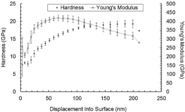
Figure 8 shows the evolutions of the hardness and Young’s modulus of the metal-lization scheme as a function of the penetra-tion depth. The Young’s modulus of the coating was calculated by first using the following equation of the contact stiffness Se: Se¼ 2 ffiffiffi p p Er ffiffiffiffiffiffiffiffiffiffiffi A hð Þc p ð1Þ The contact stiffness is dependent on the reduced Young modulus of the system holding Er. This stiffness is obtained from the unloading curve. A (hc) is the contact area as a function of the indentation depth hc. Er accounts for both the Young’s moduli, and the Poisson’s ratios of the diamond indentor (Ei, vi) and of the sample (Ee, ve). To calculate Ee, the Poisson’s ratio vewas set to 0.42.
1 Er¼ 1' n2 i Ei þ 1' n2 e Ee ð2Þ
The total penetration depth was less than the Au layer thickness, which suggests that the tip did not reach the Cr and Ti layers. Higher dispersions associated with a decrease of hardness are observed for a very small depth. The values of hardness and Young’s modulus are not reliable in this range, as the calibration of the tip fails to give reasonable values of the mechanical properties. From this point, hardness values become less scattered, until the end of the test. Figure 8 shows that a sharp increase of the mechanical properties is produced, until the end of the loading. This increase is attributed to both the strain hardening of the Au layer, and to the multilayer effect. The multilayer effect is mainly due to the gradient of mechanical properties, that is, the big difference in mechanical properties between the Au and Cr layers.
In order to determine the mechanical properties of the Cr layer, some additional nano-indentation tests were performed on a reduced Ti/Cr metallization scheme. The Figure 5. SEM observations of the indent performed on Ti/Cr/Au metallization system, (a)
morphology of the indent, (b) EDX map of the indent showing the crossed layers. (c) EDX maps showing each deposited layer separately.
Figure 6. EDX spectroscopy of the indent issued from the nano-indentation test: The tip crossed all of the deposited layers. All of the entities of the metallization system can be detected.
thickness of both Ti and Cr layers was 30 nm. Figure 9 shows that the hardness and the Young’s modulus progressively increase from 20 nm penetration depth, until reaching 20 GPa hardness and 420 GPa Young’s modulus. From 70 nm, the Young’s modulus begins to drop, until reaching 250 GPa at a penetration depth of 200 nm, which represents the overall thickness of the Cr layer. The hardness decreases at the end of the loading from 20 to 17 GPa. Since chromium is known to be highly stiff but remains brittle, this drastic decrease of the mechanical properties is essentially due to the cracks initiation in the Cr layer. This kind of event was previously avoided during nano-indentation of the Ti/ Cr/Au metallization system, as the bounding Au and Ti layers allow dampening of the interfacial shear, and thus minimize the mechanical stress in the Cr layer. This demonstrates also the effect of the Au layer on the evolution of the mechanical properties of the trilayer. In the presence of this layer, the mechanical properties keep progressively increasing until the final penetration depth, as the tip reaches only a ductile Au layer. But, when the Au layer is omitted (Figure 9), the tip directly percusses the brittle Cr layer of 50 nm thickness. In the last case, the Young’s modulus and hardness rapidly increase as the tip approaches diamond, but as soon as cracking is produced in the Cr layer, the Young’s modulus decreases. So, the difference of the
final value of the Young’s modulus is directly affected by the position of the tip within the Cr layer.
As denoted previously, the brittle Cr leads to a decrease of the Young’s modulus. Since the Cr layer is intercalated between Au and Ti and also due to its very high thinness, cracks in this layer cannot easily observed in the SEM images. Therefore, to attest the brittleness of the Cr layer, we have performed a microtension test on Cu/Ni/Cr samples with increased thickness of Cr. Diamond is replaced with a thick Cu substrate for diamond availability and cost purposes. Au is omitted to easily observe cracks. The initiation of a large number of straight surface cracks occur in the Cr coating to the view of Figure 10. These cracks are straight and equally spaced as evidenced in the micrographs embedded to the same figure. The crack initiation takes place in the Cr layer at small strains less than 2% when the stress reaches the value of 259 MPa. This attests of the brittleness of the Cr film at an earlier stage of the deformation. Then, the density of cracks increases progressively until reaching a threshold at the approach of failure. It saturates around 270 MPa of stress. At this moment, the cracks propagation mechanism is stopped, but Figure 7. Loading/unloading curves issuing from nano-indentation tests,
and performed using High precision DCM indenter.
Figure 8. Average values of the mechanical properties of the Ti/Cr/Au metallization scheme as obtained using DCM indenter.
Figure 9. Average values of the mechanical properties of the Ti/Cr metallization scheme as obtained using DCM indenter.
Figure 10. Engineering stress–strain curves with embedded SEM images showing long and straight cracks. The cracks are initiating and propagating through the Cr layer. The density of cracks increase until stabilization. A crack opening mode is occuring at the final stage of the deformation.
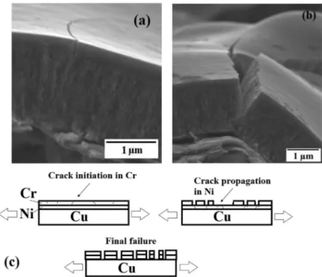
the cracks undergo a different opening mode in the direction of loading which is principally due to the higher ductility of the underlying Ni and Cu films. The inter-crack spacing stabilizes at a value of 20 mm. A more detailed SEM analysis shows first a crack propagating through the Cr film thickness due to its brittleness and leading out of the layer cracks (Figure 11a). Then, cracks pass through the nickel layer leading to a slowing down of the crack propagation and finally the total failure of the deposit (Figure 11b). A schematic representation of the failure mechanism of the layer stack is illustrated in Figure 11c.
In general, for electrical performance, there are no reference values of the Hardness and Young’s Modulus of a given deposit. However, it is suitable to have assembly materials with similar mechanical properties, especially their Young’s moduli and coefficients of thermal expansion (CTEs). These last properties have an impact on the interfacial shear stress generated in the assembly interfaces. Interfacial shear stress is a common feature produced in multilayered assemblies. Under cyclic thermal loading, interfacial shear stress increases with the mismatch of Young’s modulus and CTE. It is preferred to have a Young’s modulus, that is, close enough to those of the underlying materials (especially the joining material). The reference value of the Young’s modulus of the studied metallization system (10% max. of the metallization thickness, so as to avoid the influence of the stiffness of the substrate, and to get physically trustable data) is about 90 GPa, which is quite close to that of the conventional joining materials (including those that will be used later in this study, such as AuGe alloy or Ag nanoparticles paste).
In addition, one of the most important issues in power electronics is the electrical perfor-mance of the materials involved in the energy storage and transfer. For the moment, there is no evidence of the effect of the mechanical properties on the electrical characteristics of the diodes, such as series resistance, current density, or Schottky barrier height. Neverthe-less, several studies attest to the impact of the bias voltage on the Young’s modulus and hardness of the deposited metallic layers,[18,19]
3.2.3. Adhesion of the Ti/Cr/Au Metallization System
A good adhesion of a metallization system is principally dependent on the adhesion of the diamond chip to the attach layer (Ti in this case). For that reason and before the charac-terization of the adhesion of the whole Ti/Cr/ Au metallization system, we have performed some nano-scratching tests for the study of adhesion of Ti on C. The nano-scratching tests were carried out with the Nano Indenter XP by using a Berkovich indenter under a progres-sive load at a fixed scratching velocity of 10 mm s'1. At the end of the tests, the scratching load reached 150 mN. Figure 12 shows results of the nano-scratching tests on Figure 11. Crack initiation and propagation in the Cr and the underlying layers. (a) SEM
micrographs showing a crack initiation in the Cr layer. (b) Porpagation of the crack through the Ni layer. (c) A schematic of the fracture mechanism of the metallization system.
Figure 12. Scratch test performed on diamond substrate metallized with Titanium. (a) Morphology of the scratch. (b) Scratch profiles during and after loading.
Ti metallized diamond samples. We could observe a strong adhesion of Ti on C without any delamination or chips produced in the scratch edges as demonstrated in Figure 12a. The scratch profile during loading and after retrieval of the load is presented in Figure 12b. The deformation behavior is purely ductile and an increased elastic recovery is obtained after retrieval of the load. No real discontinuities are observed.
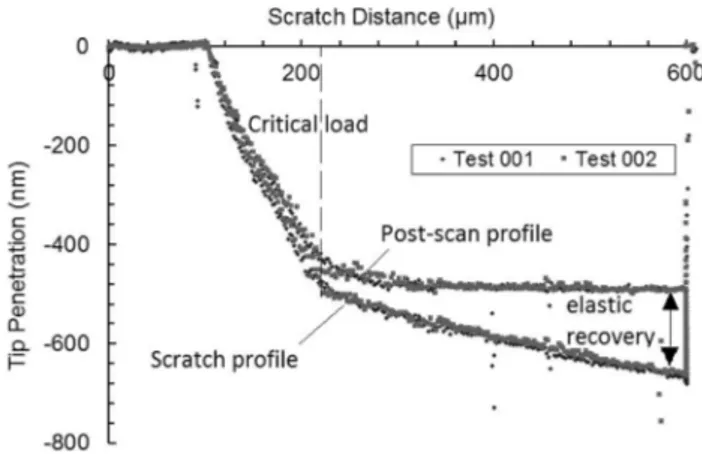
In the following, two nano-scratching tests were performed on the whole Ti/Cr/Au metallization system (tests 1 and 2) using the same conditions given previously except that the force amplitude was decreased to 80 mN. Figure 13 shows the nano-scratching curves representing the change in the penetration depth as a function of the scratching distance for the Ti/Cr/Au
metallization system. No perturbations are observed in these profiles. The curves are smooth, and the tests are reproducible. A total penetration depth of 700 nm at the end of the scratch is recorded, which is deep enough to reach the diamond. At the start of the scratch, the penetration depth matches the post-scan depth for a distance below 500 nm, indicating that the Au layer was completely scraped out. Then, the post-scan profile becomes perfectly horizontal, starting from a penetration depth of 560 nm, which corresponds to a scratching distance of 220 mm. The post-scan profile shows that the elastic recovery at the end of the test is approximately 200 nm. This displacement corresponds entirely to the elastic recovery of the diamond. A cohesive and plastic rupture of the entire layer stack was produced, exposing the diamond at the bottom of the stripe.
The adhesion test is a purely qualitative phenomenon, especially when it is assessed using nano-scratching. The morphology of the crack' its width, scratch hardness, and cross profile topography' are primordial indicators of the adhesion of the deposit. The evolution of these parameters may indicate conservative or dissipative phenomena (cracking). Figure 14a shows the morphology of the scratch. The scratch is narrow at the beginning of the test. As soon as small normal loads are initiated, the stripe depth and width increase, and the diamond is exposed (Figure 14b). The normal critical load is Lc¼ 19.2 mN, which is considered as the interfacial adhesion force of the metallization/diamond substrate. This corresponds to an indenter displacement of 220 mm, a value already highlighted on the penetration curves (Figure 13). The pile-up produced at the edge of the scratch reveals plastic deformation of the Au layer, since gold presents highly ductile behavior (Figure 14b). The present deposit does not seem to dissipate Figure 13. Scratch and post-scan profiles obtained after the
nano-scratching test performed on the Ti/Cr/Au metallization scheme.
Figure 14. Morphology of the final scratch performed on the Ti/Cr/Au metallization system, (a) micrograph of the entire scratch with embedded layer identification and characteristic distances, (b) EDX map of the scratch ending, and (c) EDX spectroscopy of the performed scratch, showing the consititutive materials of the deposit spread along the stripe edge.
energy in the interface. No chips are produced along the scratch during the nano-scratching test, attesting to the absence of cracks or delamination. The metallization has good adhesion to the diamond substrate. Figure 14b shows the EDX elemental mapping of the end of the scratch. It can be observed that the diamond substrate is exposed, and no traces of titanium are evident at the bottom of the stripe. The pile-up produced at the edges is constituted mostly of Au, but also a few traces of Cr that emerged to the surface. EDX spectroscopy analysis was performed to analyze the cross-section of the scratch. Figure 14c shows the micrograph, on which different points are localized along the scratch width, which points were selected for the determination of the chemical composition. The overall result shows high proportions of Au and C, but also some scattered Ti and Cr.
Figure 15 shows the typical topography of the residual scratches. The topography measurement represent the cross profile of the stripe. The material is deformed and compacted below the indenter. The cross profile topography shows a permanent pile-up of approximately 500 nm at both edges of the scratch, which is closely associated with the plastic deformation of Au during nano-scratching. The peak and valley profiles of this topography are almost symmetric, which attest to the ductile behavior of Au. In order to assess the material resistance to scratch, it is convenient to calculate the scratch hardness H, which is expressed as the ratio of the amplitude of the applied load to the contact area projection A. The projected area is dependent on the residual scratch width w:
H¼ f P
w2 ð3Þ
where, f is a factor dependent on the geometry of the tip. For a Berkovich indenter, f¼ 2.31. Knowing that the applied load reaches 80 mN, and that the residual width is 5 mm, the scratch hardness is H¼ 7.392 GPa.
The performed scratching tests are of great interest. Nevertheless, they remain rather qualitative. They give informa-tion about the morphology of the scratches, and the presence or absence of defects, attesting to the quality of the adhesion to the
substrate. More information can be obtained using more appropriate techniques. For example, microtension tests used on systems made up of a ductile-coated substrate could be cited, in order to analyze the mechanical stability and damage of the deposits.[20,21]These tests require various experimental meas-urements, like the tensile strength, and spacing of inter-cracks characteristic of film split-up. For single layers, the maximum shearing force interfacial, t, developed with the interface between the deposit and metal, is related to the tensile strength of the coating, s. The three-point bending test also represents an alternative to the scratching test. This test was particularly developed for the characterization of the adherence of organic coatings on titanium by Roche.[22]It provides the information on the rigidity of the system (slope of the curve forces/displacement in the linear part), on the force and maximum displacement before rupture, on the type of rupture (abrupt, or by jump), and finally on the localization and propagation of the rupture.
Some interesting characteristics, such as elastic constants and adhesion properties, can be determined using time-resolved opto-acoustic nanometrology.[23,24]This technique constitutes an interesting prospective, as it can provide mechanical properties with great precision based on photoacoustic excitation of the breathing modes of the films, and their detection, via the acousto-optic effect.
4. Conclusion
A Ti/Cr/Au metallization scheme is deposited on a heavily doped diamond substrate, and thoroughly studied. The morphology of the surface shows no defects, such as blistering or peeling, which attests to good surface quality. The metallization scheme is also tested using nano-scratching and nano-indentation experi-ments. The nano-indentation tests showed good mechanical properties of the metallization scheme, without any fracturing of the diamond substrate or the underlying layers during the lowering of the tip. Nano-scratching tests revealed a cohesive rupture of the metallization system from the first stage of the test. Unlike the previously and recently studied Ti/Pt/Au metallization scheme, the morphologies of the scratches and the indents did not show any chips. Only a few microcracks at the bottom of the stripes, perpendicular to the direction of the scratching, were produced, due to the high ductility of gold, followed by localized damage on it. These cannot be interpreted as due to poor film quality. The EDX mapping results showing the composition of the stripe termination correlate well with the scratching profiles, as they show a total scraping out of the films and the uncovered diamond. Finally, the Ti/Cr/Au metallization scheme appears to be a good alternative to the Ti/Pt/Au metallization scheme for use in power electronics applications, and can be well associated with gold-based solder alloys for the die attach.
ACKNOWLEDGEMENTS
This work was supported by the French DGE project DIAMONIX, No. 08 2 90 6066. The work was also supported by the Aerospace Valley Cluster, and the French National Research Agency ANR. The authors acknowledge the collaborative effort of the CNRS-LAAS RTB clean room team. Figure 15. Cross Profile Topography of the performed scratches showing
Conflict of Interests
The authors declare no conflict of interests.
Keywords
deposition; diamond; metallization; nano-indentation; nano-scratching; power electronics
[1] S. Msolli, J. Alexis, O. Dalverny, M. Karama, Microelectron. Reliab. 2015, 55, 164.
[2] I. Meyyappan, A. Malshe, H. Naseem, W. Brown, Thin Solid Films 1994, 253, 407.
[3] C. Johnston, P. Chalker, I. Buckley-Golder, M. van Rossum, M. Werner, E. Obermeier, Mater. Sci. Eng. B 1995, 29, 206. [4] C. Iacovangelo, Thin Solid Films 1996, 286, 264.
[5] S. C. Tjong, N. Wong, G. Li, S. T. Lee, Mater. Chem. Phys. 2000, 62, 241.
[6] S. C. Tjong, H. P. Ho, S. T. Lee, Mater. Res. Bull. 2001, 36, 153. [7] S. C. Tjong, H. P. Ho, S. T. Lee, Diamond Related Mater. 2001, 10,
1578.
[8] C. Zhen, Y. Wang, S. He, Q. Guo, Z. Yan, Y. Pu, Opt. Mater. 2003, 23, 117.
[9] H. Hoff, G. Waytena, C. Vold, J. Suehle, I. Isaacson, M. Rebbert, D. Ma, K. Harris, Diamond Related Mater. 1996, 5, 1450.
[10] A. Katz, C. Lee, K. Tai, Mater. Chem. Phys. 1994, 37, 303. [11] A. Katz, K. Wang, F. Baiocchi, W. Dautremont-Smith, E. Lane,
H. Luftman, R. Varma, H. Curnan, Mater. Chem. Phys. 1993, 33, 281. [12] S. Kon!e, G. Civrac, H. Schneider, K. Isoird, R. Issaoui, J. Achard,
A. Gicquel, Diamond Related Mater. 2010, 19, 792.
[13] S. Kon!e, H. Schneider, K. Isoird, F. Thion, J. Achard, R. Issaoui, S. Msolli, J. Alexis, Diamond Related Mater. 2012, 27–28, 23. [14] S. Msolli, J. Alexis, H. Kim, O. Dalverny, M. Karama, Thin Solid Films
2016, 619, 53.
[15] J. Achard, F. Silva, R. Issaoui, O. Brinza, A. Tallaire, H. Schneider, K. Isoird, H. Ding, S. Kon!e, M. Pinault, F. Jomard, A. Gicquel,
Diamond Related Mater. 2011, 20, 145.
[16] X. Peng, T. Clyne, Thin Solid Films 1997, 293, 261.
[17] Y. Balcaen, N. Radutoiu, J. Alexis, J.-D. Beguin, L. Lacroix, D. Sam!elor, C. Vahlas, Surf. Coat. Technol. 2011, 206, 1684.
[18] L. Bait, L. Azzouz, N. Madaoui, N. Saoula, Appl. Surf. Sci. 2017, 395, 72.
[19] A. Bendavid, P. Martin, H. Takikawa, Thin Solid Films 2000, 360, 241. [20] P. H. Wojciechowski, M. S. Mendolia, J. Vacuum Sci. Technol. A:
Vacuum, Surf. Films 1989, 7, 1282.
[21] A. Mezin, J. Lepage, N. Pacia, D. Paulmier, Thin Solid Films 1989, 172, 197.
[22] A. A. Roche, M. J. Romand, F. Sidoroff, Practical Adhesion
Measurement in Adhering Systems: A Phase Boundary Sensitive Test.
Springer US, Boston, MA 1984, p. 19.
[23] S. Peli, E. Cavaliere, G. Benetti, M. Gandolfi, M. Chiodi, C. Cancellieri, C. Giannetti, G. Ferrini, L. Gavioli, F. Banfi, J. Phys. Chem. C 2016,
120, 4673.
[24] K. M. Hoogeboom-Pot, E. Turgut, J. N. Hernandez-Charpak, J. M. Shaw, H. C. Kapteyn, M. M. Murnane, D. Nardi, Nano Lett. 2016, 16, 4773.