To cite this version :
Msolli, Sabeur and Alexis, Joël and Kim, Heung Soo and Dalverny,
Olivier and Karama, Moussa Assessment of candidate metallization systems deposited on
diamond using nano-indentation and nano-scratching tests. (2016) Thin Solid Films, vol.
619. pp. 53-60. ISSN 0040-6090
O
pen
A
rchive
T
OULOUSE
A
rchive
O
uverte (
OATAO
)
OATAO is an open access repository that collects the work of Toulouse researchers and
makes it freely available over the web where possible.
This is an author-deposited version published in :
http://oatao.univ-toulouse.fr/
Eprints ID : 16506
To link to this article : DOI :
10.1016/j.tsf.2016.10.022
URL :
http://dx.doi.org/10.1016/j.tsf.2016.10.022
Any correspondence concerning this service should be sent to the repository
administrator:
[email protected]
Assessment of candidate metallization systems deposited on diamond
using nano-indentation and nano-scratching tests
S. Msolli
a,⁎
, J. Alexis
b, H.S. Kim
a, O. Dalverny
b, M. Karama
baDepartment of Mechanical, Robotics and Energy Engineering, Dongguk University-Seoul, 30 Pildong-ro 1-gil, Jung-gu, Seoul 100-715, Republic of Korea bUniversité de Toulouse, INP/ENIT, LGP, 47, Avenue d'Azereix, F-65013 Tarbes, France
a b s t r a c t
Mechanical suitability of ohmic contacts among the select metallization systems, deposited on a p-type heavily boron-doped homoepitaxial diamond layer, was evaluated via mechanical tests on the nanoscale. Two candidate metallization systems were considered: Si/Al and Ti/Pt/Au. Metallizations were performed using two different techniques: plasma-enhanced chemical vapour deposition and “lift-off”. Effectiveness of the techniques was assessed via mechanical tests on the microscale and the nanoscale. Nano-indentation experiments were per-formed to determine the mechanical properties of the layers. Nano-scratching experiments were used to evalu-ate the mechanical adhesion on the diamond substrevalu-ate. Scanning electron microscopy was applied for observation of the morphology of the surface and the indent and for detecting defects.
Keywords: Diamond Metallization Deposition Nano-indentation Nano-scratching Power electronics 1. Introduction
Diamond is well known as a promising material for power electron-ics due to its desirable electrical and thermomechanical properties[1– 3]. Nevertheless, many technological issues must be resolved to ade-quately exploit diamond and to manufacture competitive power elec-tronic devices that can withstand high temperatures of up to 300 °C. This study focuses on diamond metallization systems that play the role of ohmic contacts. The metallization systems must satisfy many conditions, such as having the ability to withstand high voltages and current density, good mechanical properties, and good adhesion on the diamond substrate, among other requirements.
Many researchers are interested in the deposition of ohmic contacts on diamond based on the premise that good mechanical adhesion of the metallization systems is a key requirement for achieving efficient device bonding and power transmission. Refractory metals such as Ti, Mo, Ta, and W are known to form adhering carbide layers on diamond at high temperatures[4–6]. Ti-based contacts are more widely used due to the formation of a TiC layer during annealing, which enables achieve-ment of low contact resistivity and good mechanical adhesion. More-over, transition metals such as Cr, Ni, and Ni\\Cr are widely used in other multi-chip module (MCM) technologies involving Si, A1N, SiC, and alumina substrates[7]. The mechanical and electrical performances of Cr, W, Ni, and Al layers as frameworks have been investigated and
documented in the literature[8]. The ohmic contact metallization sys-tems evaluated in the studies mentioned above were deposited on a di-amond sample by the same photolithography process. It was noted that Ni is a suitable contact metallization system for utilization in high power, high temperature, and good mechanical strength diamond Schottky barrier diode applications. Nevertheless, the mechanical adhe-sion and thermal stability of these species was not investigated. The electrical capability and thermal stability after post-deposition anneal-ing of metallization systems such as C/Ti/Ni, C/Ti/Cr, and C/Ti/W have previously been investigated. Under the relevant deposition conditions of these studies, it was concluded that the adhesion of Ti/Ni to diamond is higher than that of single layer Cu due to the formation of TiC, and that only Cr is inert to AuSn during annealing[9]. Cr also offers better adhe-sion and enhances the diffuadhe-sion barrier properties (compared with Ti\\W) for Au-based conductor metallization systems on diamond sub-strates[7]. From the latter observation, it can be deduced that both the die attachment and the diffusion mechanisms are highly important for the thermomechanical stability of the assembly involving diamond. The deposition technique also appeared to be of great importance. The adhesion of sputtered Au/(Ti\\W) to diamond was significantly in-creased when the surface was activated by the sputter etch technique [7]. The electrical performance and intermetallic reaction of a Ti/Pt/Au multilayer after annealing at 800 °C and 900 °C under vacuum was also studied[10]. It was found that Au and Pt inter-diffused, but the Pt barrier was not fully consumed and effectively served as a barrier to Ti diffusion through the Au layer to the contact surface. Notably, some frameworks have been appended to Si/Al based contacts, leading to good electrical characteristics of such systems[11]. However, overall,
⁎ Corresponding author.
concrete advancements on the study of adhesion of such deposited films on diamond are rare.
Due to the lack of data concerning the mechanical and the adhesion characteristics of metallic films on diamond substrates, herein, we study some candidate metallization systems for use as ohmic contacts on dia-mond for high temperature power electronics. The ohmic contacts stud-ied here are Ti/Pt/Au and Si/Al systems. The use of a thick Si or Ti layer allows the formation of a SiC or TiC carbide layer, which ensures strong bonding. This latter point is essential if high reliability of the diamond device packaging is required. Surface morphology analyses are per-formed using scanning electron microscopy (SEM) and the energy dis-persive X-ray (EDX) technique to detect surface defects derived from deposition or annealing. Nano-indentation tests with large (XP) and small (DCM) displacements are performed to determine the elastic properties and hardness of the deposited films. Finally, the adhesion of the multilayers on the diamond substrate is evaluated using nano-scratching tests.
2. Experimental procedure 2.1. Deposition of thin films
A1.5 mm thick, heavily boron-doped diamond film deposited on the 3 × 3 × 0.5 mm lb. diamond sample used in this study. The boron den-sity in the film was approximately 3 × 1020cm− 3. The sheet resistance
of the sample was measured by four probe measurement to be about 110 Ω/□. Various metallization systems were deposited on the diamond sample by vacuum evaporation. For Si/Al metallization, a 0.2 μm Si layer was first deposited at 475 °C by plasma-enhanced chemical vapour de-position (PECVD). The metallized substrate was then annealed in a rapid thermal processing (RTP) furnace at 1200 °C under vacuum for 10 s prior to cleaning with hydrofluoric acid to remove any oxides on the surface, including the native SiO2. The purpose of this operation is
to form a silicon carbide layer at the interface between silicon and dia-mond. This layer was used to help to ensure good adhesion of the layer stack on diamond. Upon completion of this operation, a 0.5 μm thick Al film was formed by the photolithography technique or by “lift-off”. This step was followed by annealing at 450 °C for 20 min in a tubular passage furnace to improve the adhesion of the metallization system.
On the second diamond substrate, a Ti/Pt/Au multilayer was formed by “lift-off”, where the multilayer comprised respective layers with thicknesses of 0.1, 0.05, and 0.5 μm. Once these films were obtained, the sample was annealed at 450 °C for 30 min. This is the minimum temperature at which Ti and Si form a carbide layer with diamond[11]. 2.2. Mechanical characterization
2.2.1. Nano-indentation tests
The mechanical properties of the layers, such as the stiffness and hardness, were determined by using an MTS© nano-indentation device equipped with a Berkovich pyramidal indenter. This type of device can continuously measure the stiffness of the contact via “Continuous Stiff-ness Measurement”. Nano-indentation tests with small and large dis-placements were carried out at room temperature (23 °C) depending on the thickness of the deposited films. The test conditions are specified inTable 1. For large displacements, the tests were performed with an MTS XP nano-indenter in dynamic mode, making it possible to obtain the overall Hardness and Young's Modulus values of the multilayer. However, the DCM nano-indenter was utilized for small displacement (400 nm). The DCM nano-indenter permits determination of the indi-vidual properties of the films with quite good precision. The mechanical properties of the layers, such as the hardness and elastic modulus, were determined via the common Oliver-Pharr method[12]. For more details about the nano-indentation technique, one can refer to papers by Alexis or Msolli and co-workers[13–15], for instance.
2.2.2. Nano-scratching tests
The adhesion of the deposited multilayers was also assessed using nano-scratching tests. The test parameters were adapted depending on the thickness of the metallization layer (see Table 2). Nano-scratching tests were performed on the sample surface by moving a Berkovich tip in three successive steps and measuring the penetration depth. The first step was carried out to determine the surface topogra-phy and to correctly set the position of the indenter. The aim of the sec-ond step was to scratch the sample surface. The applied load was then increased progressively up to a maximal value and subsequently re-duced. Finally, the spring-back and the topography of the residual scratch were measured from a last scan using a small applied load.
2.2.3. Morphology and EDX analysis
Observations were carried out with a field emission gun scanning electron microscope (FEG SEM-7000F from JEOL with the incident elec-tron beam maintained between 10 and 15 kV) to analyse the surface morphology of the films. The analysis was corroborated by chemical analysis with an SDD Bruker X flash energy dispersive X-ray spectrom-eter (EDX).
3. Study of Si/Al metallization system 3.1. Morphology of the surface
Fig. 1shows micrographs obtained by scanning electron microscopic (SEM) analysis of the metallization surface at various magnifications ranging from ×500 to ×50,000. The Si/Al multilayer did not have any detectable defects. The Si/Al multilayer appeared relatively dense and homogeneous at low magnification. Observations at higher magnifica-tion revealed the presence of clusters of a few microns, evenly distribut-ed on the sample surface (Fig. 1a). The microstructure of the deposited Al comprised equiaxed grains with diameters of 100 nm (Fig. 1b).
EDX spot analyses were carried out on the metallization surface. The overall spectrum attests the presence of two layers of aluminium and silicon in region 3 (Fig. 1a). Indeed, the “interaction pear” of the SEM in-cident beam has a depth greater than the deposition thickness of alu-minium, which also explains the detection of the sub-Si layer. However, the previously observed clusters denoted as region 4 (Fig. 1a) are those of aluminium because the Al content is higher than the Si content.
Table 1
Operating conditions for nano-indentation tests.
Berkovich tip nature DCM XP
Load resolution 1 nN 100 nN
Column displacement resolution 0.05 nm 0.1 nm
Number of tests 30 10
Displacement into the surface 400 nm 2 μm
Approach velocity 8 nm/s 8 nm/s
Distance between nano-indents 10 μm 50 μm
Table 2
Operating conditions for nano-scratching tests.
Distance between scratches 500 μm
Scratch length 700 μm Scratching velocity 10 μm/s Topography load 0.1 mN Scratching load 0.1 mN to 80 mN Final load 0.1 mN Number of scratches 2 − 3
3.2. Mechanical properties of Si/Al system 3.2.1. Nano-indentation with MTS XP indenter
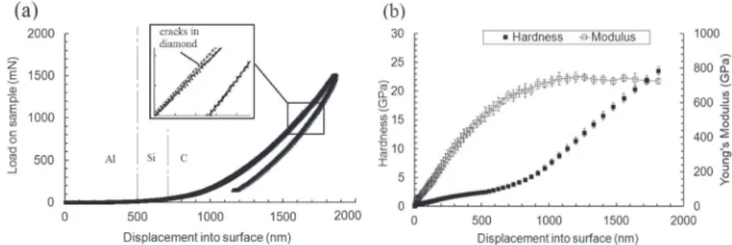
To obtain a scatter in the data, ten nano-indentation tests were per-formed with an imposed depth of 2 μm. Nano-indentation tests at large displacement (where the maximum load reached 1500 mN) were use-ful for determining the variation of the mechanical properties of the Si/ Al multilayer with the indented depth.Fig. 2a shows the load evolution as a function of the penetration into the surface for all the tests. Good re-peatability of the load displacement responses was observed. To facili-tate interpretation of the curves, the nature of the different layers that were reached and their thicknesses are shown directly on the graph. Each load curve can be divided into three distinct parts.
The first part appears linear and is located between the loading start and a penetration depth close to 500 nm. It is characterized by the low-est slope for the entire load curve. This is explained by the fact that the stiffness and hardness of Si and Al are much smaller than those of dia-mond. The second portion corresponds to a transition and ranges be-tween 500 nm and 1300 nm, where the influence of diamond becomes more important. Over 1300 nm, the influence of metallization becomes negligible and the applied load increases sharply due to the very high hardness of diamond.
Fig. 2b shows the average stiffness and hardness curves as functions of the indentation depth. The Young's modulus increased progressively from the start of the response to reach a plateau at 750 GPa from a pen-etration depth of 1100 nm. The highest dispersion observed at the end of the test and the slight decrease of the load, are due to initiation of cracking of the diamond substrate, which begins from an indentation depth of 1500 nm. This crack is confirmed by the flat portions present on the load displacement curves (seeFig. 2a).
As shown in the same figure, the hardness evolved differently, where it increased very slightly up to a penetration depth of 600 nm. This was followed by a rapid increase above 600 nm to reach a value of 25 GPa. These initial results do not permit determination of the stiff-ness and hardstiff-ness of each layer, considering the influence of the
diamond substrate at this stage. It is interesting to note that the influ-ence of the diamond substrate on the stiffness calculation emerges faster (even at small loads) than on the hardness determination. This has previously been observed for other coated substrates[16]. The hard-ness and stiffhard-ness of the diamond substrate appear to be respectively equal to 25 GPa and 750 GPa. Other studies of the mechanical properties reported values for thick diamond coatings deposited on WC substrates close to that found herein[17,18].
The nano-indents relevant for these curves were observed by scan-ning electron microscopy (SEM) to confirm the previous analyses.Fig. 3shows the morphology of the nano-indent and the indented layers. Microcracks were noticeable in the diamond substrate (Fig. 3a). The nano-indent had a notable “barrel-shaped” form on its edges, resulting from incompressible plastic deformation and the up-flow of the alumin-ium layer around the indenter. This “pile-up” against the indenter faces is characteristic of work-hardened materials such as aluminium. Assess-ment of the pile-up is important because pile-up leads to differences be-tween the true contact area and the apparent contact area, which is usually observed after indentation. In this case, the indented material appears to be stiffer. The advantage of continuous stiffness measure-ment (CSM) is that it takes into account the instantaneous variation of the contact area by use of particular values of some adjusting parame-ters (see Ref.[19]and[20]for the meaning and details of the contact area calculations). During testing, all the layers are crossed, as shown by EDX mapping (seeFig. 3b and EDX profilometry on bottom of the nano-indent; seeFig. 4).
3.2.2. Nano-indentation with DCM indenter
The large displacement nano-indentation tests did not permit deter-mination of the intrinsic mechanical properties of the aluminium layer. Only the properties of the diamond substrate were estimated. There-fore, small displacement nano-indentation tests were carried out with the dynamic control module (DCM) nano-indenter MTS that offers bet-ter resolution even at small applied loads due to its lower stiffness.
Fig. 1. Si/Al surface micrographs obtained by SEM observation at different magnifications. (a) 6000 and (b) × 50,000.
Fig. 5a shows the load evolution with the imposed penetration depth of the indenter (the maximum depth was 400 nm). The load profiles do not show any discontinuities despite the significant dispersion, mainly due to the higher sensitivity of the DCM tip to the surface roughness. The spring-back was very small (b20 nm). This is mainly due to the small yield strength of Al, associated with its significant plastic deforma-tion. Since DCM type indenter is highly sensitive, creep displacements are observed during the holding load segment. Indeed, during the hold, the indenter continues to penetrate into the surface. Subsequently, the area of the indent increases. For the studied metallization, the dis-placement creep reaches 40 nm at room temperature.
The curves of the average hardness and elastic stiffness module as a function of the penetration depth are shown inFig. 5b. The stiffness was stabilized at 70 GPa for indentation depths ranging from 40 to 60 nm, which is just one-tenth of the Al film thickness. The influence of Si and diamond was small at this depth. However, over 80 nm, the measured stiffness increased progressively because of the influence of the dia-mond substrate. Therefore, the stiffness and hardness of the Al layer could be estimated as 70 GPa and 1 GPa respectively. Other studies pro-vide reference values consistent with the modulus values found herein. The hardness values also remained very close to bibliographical results [21].
3.2.3. Nano-scratching tests
The adhesion of the Si/Al bilayer was evaluated via nano-scratching tests according to the experimental conditions described inTable 2. The penetration depth and the dimensionless friction coefficient were de-termined with respect to the scratch distance (Fig. 6).
The nano-scratching tests provide comparable and reproducible profiles regardless of the location of the preformed scratches (Fig. 7). The behaviour was initially linear with a constant penetration rate of − 2 nm·μm− 1. This behaviour is mainly due to the ductile and rather hard Al layer. Once the diamond substrate was reached, an abrupt
change of the penetration rate occurred, but the profile remained linear. For depths below 500 nm, the topographic profile of the final scan matched the penetration profile during scratching. This indicates that the Al layer undergoes substantial plastic deformation as during the in-dentation tests. Over the stated depth, the topographic profile becomes different from that measured during scratching. The gap between the two profiles could reach a maximum of about 160 nm at the end of scratching, which corresponds to the diamond elastic spring-back that represents 20% of the total strain at maximum load.
The evolution of the friction coefficient as a function of the penetra-tion distance is shown inFig. 6b. The friction coefficient, μ, is the ratio of the lateral versus the normal force imposed by the indenter. This coeffi-cient increased sharply when the tip began to penetrate the Al layer, reaching a value of 0.3 at a scratching distance of 180 μm (penetration depth equal to −304 nm, normal load equal to 12.92 mN). At this nor-mal load, a slight perturbation of the friction coefficient was observed, indicative of different mechanical behaviour due to the removal of Al chips during scratching. Thus, the friction coefficient continued to in-crease to reach a value of 0.5 when the indenter reached the Si/Al inter-face. Finally, the friction coefficient began to fall and stabilize at a value of around 0.23 at the end of the test when the tip reached the diamond substrate.
Fig. 7shows the morphology of the two scratches formed on the Si/ Al bilayer. From the beginning of the scratching process, the Al film underwent plastic deformation due to its low hardness, with “bead” for-mation on the edges. At the end of the scratching, initial forfor-mation of chips was observed due to the cohesive failure of Al. This damage con-firms the evolution of the recorded friction coefficient and the abrupt topography variations. No delamination or chip formation was observed when the tip passed through the silicon layer, evidencing therefore, the good adhesion of this layer to diamond. This result was also confirmed by the gradual evolution of the friction coefficient when the tip passed through the Si layer and scratched the diamond.
Fig. 3. Nano-indent obtained from nano-indentation test on Si/Al metallization system; (a) SEM micrograph of the deformation morphology showing cracks in diamond and (b) EDX mapping showing the composition of the multilayer.
Fig. 4. Chemical analyses using EDX profilometry of the nano-indent formed on Si/Al multilayer. (a) Morphology of the indent and the direction of analysis and (b) compositions along the chosen analysis direction.
4. Study of Ti/Pt/Au metallization system 4.1. Morphology of the surface
The micrographs acquired at low magnification show defect reparti-tion over the entire sample surface (Fig. 8). These defects are either blis-ters with diameblis-ters varying between 5 and 30 μm or peeling of the metallization species. From the micrographs obtained at higher magni-fication, the average grain size of the Au film was determined as 2 μm. These defects appear to be generated during the deposition process. Blisters often result from the presence of residual stresses in the layers and/or brittle interfacial areas.
In order to determine the location of these defects, EDX analyses were performed. The composition of the layers and origin of the defects on the surface were determined by chemical analysis of two character-istic zones of the sample surface: a defect-free zone (region 1) and an area corresponding to peeling (region 2) (Fig. 8).
Chemical analysis of region 1 shows the presence of a gold layer on the substrate surface. The other layers were not detected due to their low thickness with respect to the gold layer. Conversely, chemical anal-ysis of region 2 revealed only the presence of carbon, corresponding to diamond. Peeling seemed to be localized between Ti and diamond or between Pt and Ti. Several EDX analyses were performed in the peeling areas using incident electrons at small acceleration voltages (~ 5 kV). The aim was to analyse thin layers while maintaining a correct statistical measurement by performing long acquisitions. For the analyses carried out in the peeling areas, only carbon was highlighted. However, it is dif-ficult to precisely decide on the peeling area in view of the low thick-nesses of the Ti and Pt layers. During the deposition process, non-negligible compressive residual stress was produced in the Ti/C inter-face. When the stress in the metallization system is compressive, buck-ling-driven interface delamination occurs, as observed for the Ti/Pt/Au metallization system.
4.2. Mechanical properties of Ti/Pt/Au system 4.2.1. Nano-indentation with MTS XP indenter
Fig. 9a shows the corresponding loading-unloading curves for tests performed on the diamond substrate with the Ti/Pt/Au metallization
system. The test results were reproducible. The general shape of the curves was similar to that of those already described for Si/Al metalliza-tion on diamond. The load increased slightly in the first stage due to the low stiffness and hardness of gold. As previously observed, no influence of the intermediate layers of Ti and Pt was observed because of the thin-ness of these layers. The load increased rapidly to reach a maximum depth of 1600 nm at the end due to the high stiffness of the diamond substrate. The elastic spring-back represents nearly 50% of the total pen-etration distance. This is higher than that observed for Al/Si metalliza-tion. The present value is mainly due to the spring-back of the diamond substrate.
Fig. 9b shows the change in the stiffness and hardness of the system as a function of the penetration depth. Due to the progressive increase of the depth from gold to diamond, the stiffness increased to reach a max-imum value of about 750 GPa, which is greater than that found for the Si/Al metallized substrate. This value corresponds to the Young's modu-lus of diamond. From this depth (600 nm), the stiffness decreased con-siderably with many perturbations, the origin of which is certainly related to the appearance of cracks within the diamond substrate itself, as seen above. However, the hardness continued to increase to a maxi-mum average value of 26 GPa, which is very close to the value deter-mined for the Si/Al metallized substrate.
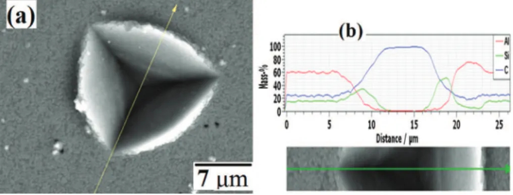
The observation of the nano-indent morphology shows the presence of three cracks (Fig. 10a). These cracks appeared on the faces that were in contact with the indenter and propagated to the edges (~ 3 μm). These cracks were separated from the nano-indent centre by 500 nm. All of the obtained nano-indents were characterized by these cracks on their inner faces. Mapping showed that the apparent surface in the centre was predominantly that of diamond. Due to its low thickness, the Pt layer (0.05 μm) was not detectable.
Pile-up occurred during plastic deformation of the ductile Au, and superposed plies were observed at the crater edges. This is expected due to the strain hardening nature of Au. The pile-up tends to increase the contact area of the indenter and to enhance the gradient of plastic deformation.
The chemical composition of the nano-indent throughout the sec-tion was determined as shown inFig. 11. These chemical analyses con-firm the location of the cracks in diamond based on consideration of the size of the zone in contact with diamond.
Fig. 5. Nano-indentation data for the Si/Al multilayer using DCM-type tip. (a) Loading/unloading curves and (b) average hardness and Young's modulus against penetration into surface.
4.2.2. Nano-indentation with DCM indenter
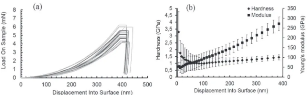
Nano-indentation tests at small displacements were carried out to characterize the intrinsic properties of the surface gold layer (Fig. 12a). The behaviour of the metallization species was almost plastic given the very small spring-back measured during unloading. In fact, this spring-back is too small compared to the maximum penetration depth. In addition, creep displacement is produced at the hold but it is not as significant as the one observed for the Si/Al metallization. Dis-placement creep is not exceeding 15 nm.
Fig. 12b shows the changes in the average mechanical properties as a function of the penetration depth. A plateau was logged for a depth of 40 nm. This plateau corresponds to the intrinsic properties of the gold layer; the stiffness was nearly 80 GPa and the hardness was close to 1 GPa.
4.2.3. Nano-scratching tests
The scratching profiles obtained during the tests performed on the Ti/Pt/Au multilayer are shown inFig. 13a. The profile indicates that the penetration depth increased rapidly until the end of the scratch when it reached the diamond substrate. The profile of the “post scan” shows that the spring-back started very early during scratching and corresponded to that of the entire metallization system with diamond. This spring-back was very high compared to the one obtained for the Si/Al metallization system and represents more than the half of the total penetration depth at the end of the test. However, the profile of the “post scan” became irregular and fluctuated in the middle of the scan. SEM observations are required to understand these variations.
The friction coefficient increased rapidly to 0.6 when the indenter crossed gold and platinum, then decreased and stabilized at 0.25 when the diamond substrate was reached (Fig. 13b).
The morphology of the scratches formed on the Ti/Pt/Au multilayer is shown inFig. 14. The beads on the edges of the scratch were obtained due to the ductility of gold. Peeling of the multilayer occurred from a scratch distance of 160 μm, even before the tip reached the diamond substrate. At this distance, the indenter was at a depth corresponding to the thickness of Ti for a critical scratch load of about 25 mN. These variations appeared due to the deformation of the multilayer, and par-ticularly due to the mechanically affected Ti/C interface. At a scratch dis-tance of over 230 μm, the ductile fracture continued to the end of the scratch.
5. Conclusion
The Si/Al metallization system had a uniform morphology with some Al clusters evenly distributed on the surface. The Al surface com-prised grains with uniform diameters. Changes in the stiffness and hard-ness of the bilayer against the penetration depth were determined by a nano-indentation test. The mechanical properties of aluminium (Hal=
1 GPa and Eal = 70 GPa) and diamond (HC= 25 GPa and EC =
750 GPa) were determined. It was not possible to determine the me-chanical properties of the Si layer given its low thickness and because this layer was sandwiched between two materials with strong mechan-ical properties. A significant creep displacement was noticed at room
Fig. 7. SEM Micrographs showing the morphology of the scratches formed on Si/Al bilayer.
Fig. 8. Ti/Pt/Au surface micrographs obtained by SEM observations at different magnifications. The micrographs show the presence of several blisters of constant size over the surface and peeling occurred due to compressive stress.
temperature during the hold time. This creep displacement attests of a viscoplastic behaviour of the metallization system. Moreover, due to the ductile nature of Al, a pile-up phenomenon was observed on the edges of the indent leading to significant plastic deformation. Nano-scratching tests showed that the failure in aluminium is cohesive; the interface strength can therefore be taken as being greater than the shear strength of aluminium. The silicon layer appears to adhere well to the diamond substrate due to formation of a SiC interphase at the in-terface during heat treatment, as previously documented in many studies.
Unlike Si/Al metallization systems, the diamond substrate with the Ti/Pt/Au metallization system has many defects distributed on its sur-face, formed by blistering or peeling. EDX spectrometric analysis indi-cated that peeling of the layers possibly occurred at the Ti/C interface, involving a buckling-driven interface delamination mechanism. High load nano-indentation tests revealed the presence of cracks on the nano-indents. These cracks initiate within the diamond substrate and
propagate to the metallization system, as shown by EDX spectrometric analysis and indent micrographs. The intrinsic mechanical properties of the gold layer and diamond were determined as HAu= 1 GPa,
EAu= 80 GPa, HC= 26 GPa, and EC= 750 GPa. Unlike the Si/Al
metalli-zation system, Ti/Pt/Au metallimetalli-zation system exhibits small creep dis-placement. Nano-scratching tests reveal the brittleness of the Ti/C interface, indicated by the formation of several chips on the scratch edge when the tip reached the Ti layer.
Acknowledgments
This work was supported by the French DGE project DIAMONIX, No. 08 2 90 6066. The authors thank LAAS-CNRS laboratory for its role in the fabrication of the diamond metallization systems. Special thanks to Pr. Jacques Debard from JEAN DUPUY College for assistance with deposi-tion of the metallizadeposi-tion systems.
Fig. 9. Nano-indentation data for the Ti/Pt/Au multilayer using XP-type tip. (a) Loading/unloading curves and (b) average hardness and Young's modulus against penetration into surface.
Fig. 10. Nano-indent obtained from nano-indentation test performed for Ti/Pt/Au metallization system: (a) SEM micrograph of the deformation morphology and (b) EDX mapping showing the composition of the multilayer.
Fig. 11. Chemical analyses using EDX profilometry of the nano-indent formed on Ti/Pt/Au multilayer. (a) Morphology of the indent and the direction of analysis and (b) compositions along the chosen analysis direction.
References
[1] J. Achard, F. Silva, R. Issaoui, O. Brinza, A. Tallaire, H. Schneider, K. Isoird, H. Ding, S. Koné, M. Pinault, F. Jomard, A. Gicquel, Thick boron doped diamond single crystals for high power electronics, Diam. Relat. Mater. 20 (2011) 145–152.
[2] S. Koné, G. Civrac, H. Schneider, K. Isoird, R. Issaoui, J. Achard, A. Gicquel, {CVD} di-amond schottky barrier diode, carrying out and characterization, Diam. Relat. Mater. 19 (2010) 792–795.
[3] H. Ding, K. Isoird, H. Schneider, S. Kone, G. Civrac, Basic parameters and models in simulation of {CVD} diamond devices, Diam. Relat. Mater. 19 (2010) 500–502. [4] Y. Zhu, B. Zheng, W. Yao, L. Cao, The interface diffusion and chemical reaction
be-tween a Ti layer and a diamond substrate, Diam. Relat. Mater. 8 (1999) 1073–1078. [5] T. Tachibana, B. Williams, J. Glass, Correlation of the electrical properties of metal contacts on diamond films with the chemical nature of the metal-diamond inter-face. II. Titanium contacts: a carbide-forming metal, Phys. Rev. B 45 (1992) 11975. [6] M. Yokoba, Y. Koide, A. Otsuki, F. Ako, T. Oku, M. Murakami, Carrier transport mech-anism of ohmic contact to p-type diamond, J. Appl. Phys. 81 (1997) 6815–6821. [7] I. Meyyappan, A.P. Malshe, H.A. Naseem, W.D. Brown, Au/(Ti-W) and Au/Cr
metalli-zation of chemically vapor-deposited diamond substrates for multichip module ap-plications, Thin Solid Films 253 (1994) 407–412.
[8] S. Koné, H. Schneider, K. Isoird, F. Thion, J. Achard, R. Issaoui, S. Msolli, J. Alexis, An assessment of contact metallization for high power and high temperature diamond schottky devices, Diam. Relat. Mater. 27–28 (2012) 23–28.
[9] S. Tjong, H. Ho, S. Lee, Development of single- and multi-layered metallic films on diamond by ion beam-assisted deposition, Diam. Relat. Mater. 10 (2001) 1578–1583.
[10] H. Hoff, G. Waytena, C. Vold, J. Suehle, I. Isaacson, M. Rebbert, D. Ma, K. Harris, Ohmic contacts to semiconducting diamond using a Ti/Pt/Au trilayer metallization scheme, Diam. Relat. Mater. 5 (1996) 1450–1456.
[11] M. Werner, C. Johnston, P. Chalker, S. Romani, I. Buckley-Golder, Electrical character-isation of Al/Si ohmic contacts to heavily boron doped polycrystalline diamond films, J. Appl. Phys. 79 (1996) 2535–2541.
[12] W. Oliver, G. Pharr, An improved technique for determining hardness and elastic modulus using load and displacement sensing indentation experiments, J. Mater. Res. 7 (1992) 1564–1583.
[13] J. Alexis, B. Etcheverry, J. Beguin, J. Bonino, Structure, morphology and mechanical properties of electrodeposited composite coatings Ni-P/SiC, 2010. Mater. Chem. Phys. 120 244–250 ([Online]. Available: http://www.sciencedirect.com/science/arti-cle/pii/S0254058409007597).
[14] J. Alexis, C. Gaussens, B. Etcheverry, J.-P. Bonino, Development of nickel-phosphorus coatings containing micro particles of talc phyllosilicates, Mater. Chem. Phys. 137 (2013) 723–733.
[15] S. Msolli, J. Alexis, O. Dalverny, M. Karama, Experimental characterization of the me-chanical behavior of two solder alloys for high temperature power electronics appli-cations, Microelectron. Reliab. 55 (2015) 164–171.
[16] N. Chechenin, A ‘hydrostatic core’ model of elastic deformations in an indented film/ substrate system, Thin Solid Films 304 (1997) 78–84.
[17] L.D. Fazio, S. Syngellakis, R. Wood, F. Fugiuele, G. Sciumé, Nanoindentation of {CVD} diamond: comparison of an {FE} model with analytical and experimental data, Diam. Relat. Mater. 10 (2001) 765–769.
[18] N. Savvides, T. Bell, Hardness and elastic modulus of diamond and diamond-like car-bon films, Thin Solid Films 228 (1993) 289–292.
[19] S. Bec, A. Tonck, J.M. Georges, E. Georges, J.L. Loubet, Improvements in the indenta-tion method with a surface force apparatus, Philos. Mag. A 74 (1996) 1061–1072. [20] N. Fujisawa, M.V. Swain, Effect of unloading strain rate on the elastic modulus of a
viscoelastic solid determined by nanoindentation, J. Mater. Res. 21 (2006) 708–714. [21] N. Sakharova, J. Fernandes, J. Antunes, M. Oliveira, Comparison between Berkovich, Vickers and conical indentation tests: A three-dimensional numerical simulation study, Int. J. Solids Struct. 46 (2009) 1095–1104.
Fig. 12. Nano-indentation data for the Ti/Pt/Au multilayer using DCM-type tip. (a) Loading/unloading curves and (b) variation of hardness and Young's modulus against penetration into surface.
Fig. 13. Nano-scratching data for the deposited Ti/Pt/Au multilayer. (a) Depth profiles and (b) variation of the friction coefficient during the scratch test.