HAL Id: tel-01808874
https://tel.archives-ouvertes.fr/tel-01808874
Submitted on 6 Jun 2018HAL is a multi-disciplinary open access archive for the deposit and dissemination of sci-entific research documents, whether they are pub-lished or not. The documents may come from teaching and research institutions in France or abroad, or from public or private research centers.
L’archive ouverte pluridisciplinaire HAL, est destinée au dépôt et à la diffusion de documents scientifiques de niveau recherche, publiés ou non, émanant des établissements d’enseignement et de recherche français ou étrangers, des laboratoires publics ou privés.
Test and characterization methodologies for advanced
technology nodes
Darayus Adil Patel
To cite this version:
Darayus Adil Patel. Test and characterization methodologies for advanced technology nodes. Elec-tronics. Université Montpellier, 2016. English. �NNT : 2016MONTT285�. �tel-01808874�
Délivré par Université de Montpellier
Préparée au sein de l’école doctorale I2S
Et de l’unité de recherche LIRMM
Spécialité : SYAM
Présentée par DARAYUS ADIL PATEL
Soutenue le 5 Juillet 2016 devant le jury composé de M. Daniel CHILLET Professeur, Université de
Rennes
Président du Jury / Rapporteur
M. Salvador MIR Directeur de Recherche CNRS, TIMA
Rapporteur Mme. Sylvie NAUDET Team Leader,
STMicroelectronics
Examinateur M. Alberto BOSIO MCF HDR, Université de
Montpellier
Examinateur M. Patrick GIRARD Directeur de Recherche
CNRS, LIRMM
Directeur de Thèse M. Arnaud VIRAZEL MCF HDR, Université de
Montpellier
co-Directeur de Thèse
Mme. Béatrice PRADARELLI PAST, Université de Montpellier
Membre Invitée
TEST AND CHARACTERIZATION
METHODOLOGIES FOR ADVANCED
TEST
AND
CHARACTERIZATION
METHODOLOGIES
FOR
ADVANCED
TECHNOLOGY
NODES
Presented by
Darayus Adil Patel
STMicroelectronics
Laboratoire d'Informatique, de Robotique et de Microélectronique de Montpellier
Université de Montpellier
This dissertation is submitted for the degree of Doctor of Philosophy July 2016
Dedicated to my Beloved Parents and
ABSTRACT
The introduction of nanometer technologies, has allowed the semiconductor industry to create nanoscale devices in combination with gigascale complexity. However, new technologies bring with them new challenges. In the era of large systems embedded in a single System-On-Chip and fabricated in continuously shrinking technologies, it is important to test and ensure fault-free operation of the whole system. The cost involved in semiconductor test has been steadily growing and testing techniques for integrated circuits are today facing many exciting and complex challenges. Although important advances have been made, existing test solutions are still unable to exhaustively cover all types of defects in advanced technology nodes. Consequently, innovative solutions are required to cope with new failure mechanisms under the constraints of higher density and complexity, cost and time to market pressure, product quality level and usage of low cost test equipment.
The work of this thesis is focused on the development of silicon test and characterization methodologies that aid in the accurate detection and resolution of issues that may arise due to variability, manufacturing defects, wear-out or interference. A wide spectrum of these challenges has been addressed from a test perspective to ensure that the availability of effective test solutions does not become a bottleneck in the path towards further scaling. Additionally the advances and innovations introduced in the myriad domains of electronic design, reliability management, manufacturing process improvements etc. that call for the development of advanced, modular and agile test methodologies have been effectively covered within the scope of this work.
This manuscript presents the significant contributions made for enabling resolution of state of the art industrial test challenges via the design and implementation of novel test strategies (targeting the 28nm FDSOI technology node) for:
· Detection & diagnosis of timing faults in standard cells. · Analysis of Setup and Hold margins within silicon.
· Verification & reliability analysis of innovative test structures. · Analysis of on-chip self heating.
ACKNOWLEDGEMENTS
“If I have seen further than others, it is by standing upon the shoulders of giants.”
Issac Newton
First and foremost, I would begin by thanking my Lord, the Almighty, for holding my hand and showing the path ahead throughout the course of my thesis. Only due to His countless gifts of sense, intellect, patience, health, family and many more, could I complete this task. Thank you for the strength you have given me and all the wonderful people around me who made the past three years truly meaningful.
During my time at STMicroelectronics, I was extremely fortunate to have had the opportunity to learn and grow under the tutelage of my super amazing ‘Maman’, Dr. Sylvie Naudet during the development of this work. I would like to gratefully and sincerely thank Sylvie for her care, understanding, patience and most importantly friendship during the course of my thesis from inception to completion. Despite her busy schedule, Maman always kept a watchful eye over me and provided me with her invaluable guidance whenever needed. To synthesize, I consider myself truly privileged to have had this opportunity to grow my intellectual prowess, sharpen my critical thinking and understand the subtle nuances of the game of life under her umbrella.
I am very grateful to my Professors Patrick Girard, Arnaud Virazel & Alberto Bosio for their guidance, support and regular feedback throughout the course of my thesis. Also for their thought-provoking ideas and helpful criticism in improving the quality of this manuscript and other publications. Working at LIRMM under their supervision, helped me to understand and better appreciate the academic essence of any project. I am thankful for their time, efforts and constant interaction all along. Their invaluable advises helped keeping my research well directed while maintaining my autonomy.
Perhaps I owe my largest quantum of gratitude to the truly awesome team that I was lucky to be part of at ST Crolles. Thank you Daniel Noblet for being the huge pillar of strength that you have been for me all throughout and the ginormous force of positivity that you are. Thank you Fabien for being a great Mentor and friend. While learning from you I have always been inspired by your attitude, zeal and enthusiasm
towards any given task. Thank you Damien Croain & Daniel Caspar for always being there to shine light upon any technical darkness that befell me. Your mere presence gave me the confidence that the solution to any problem could be mined out of your mountains of knowledge. Merci beacoup my ‘Queen’ Françoise for your camaraderie and royal influence. Many thanks to David Meyer & David Bonciani for being the great friends that you are to me. I shall always greatly appreciate and fondly remember all your support and help. Thank you Julien Berger for always being accommodating and helpful. Thank you Robert ‘Bob’ Seilles for teaching me among many things that there is a great deal more to life than just work. Thank you Loïc for always being Good. Being part of such a wonderful team greatly accelerated my learning curve and made life a joyful journey.
A special word of thanks goes to Deepak Kumar Arora & Kapil Juneja at ST Noida. It was an enriching experience working with them as I benefited from their clarity of thought and lucidity in explanation. Despite their hectic workloads they were always available to have discussions and help me solve my doubts. I would also like to acknowledge all the other people with whom I had the pleasure and privilege of collaborating with. They are Abhishek Jain, Rajesh Kumar Immadi, Sujatha Balaraman, Philippe Brahic, Sylvain Clerc, Fady Abouzeid, Franck Gardik, Jeff Nowakowski, Guy Bossan, Shahabuddin Qureshi, Fabrice Carite, Manoubi Bourabei, Gilles Lievre, Dennis Roche, Vincent Huard and Robin Wilson.
I would also like to express my gratitude to two of my most cherished friends Giulio & Giulio with whom I shared the path during these last three years. Words are not enough to describe them, they are really extraordinary. Thank you for the great support in the moments when I needed help, for all the great time that we have spent together and most of all for your friendship. Also a big thank you to Anu Asokan, Imran Wali, Aymen Touati, Alejandro Nocua & Amit Karel at LIRMM for their warm friendships and companionship.
And at last, but certainly not the least, thanks to my parents who have never lost their faith in me and have always supported me in every decision I took, no matter how far away from home it has taken me. Their constant support and strength has aided and encouraged me throughout this endeavor. I shall forever remain indebted for your love and sacrifice.
TABLE OF CONTENTS
ABSTRACT ... I ACKNOWLEDGEMENTS ... III TABLE OF CONTENTS ... V LIST OF FIGURES ... IX LIST OF TABLES ... XIII LIST OF ABBREVIATIONS ... XV
INTRODUCTION ... 1
1 CONTEXT AND THESIS OBJECTIVES ... 5
1.1SEMICONDUCTOR TECHNOLOGY EVOLUTION ... 6
1.2CHALLENGES IN ADVANCED TECHNOLOGY NODES ... 6
1.2.1 Variability ... 7
1.2.2 Manufacturing Defects ... 8
1.2.3 Wear-out ... 8
1.2.4 Interference ... 9
1.3FDSOITECHNOLOGY NODE ... 9
1.4TESTING OVERVIEW ... 10 1.4.1 Characterization Test ... 11 1.4.2 Production Test ... 12 1.4.3 Burn-in Test ... 12 1.4.4 Incoming Inspection ... 13 1.5RESEARCH OBJECTIVES ... 13
2 AN EFFECTIVE POWER-AWARE AT-SPEED TEST METHODOLOGY FOR IP QUALIFICATION AND CHARACTERIZATION ... 17
2.1INTRODUCTION ... 18
2.2BACKGROUND AND MOTIVATIONS... 19
2.3CIRCUIT DESIGN ARCHITECTURE AND IMPLEMENTATION ... 22
2.4TEST METHODOLOGY ... 25
2.4.2 Test Flow ... 28
2.5EVALUATION OF THE PROPOSED TEST METHODOLOGY ... 30
2.5.1 Memory and Runtime Evaluation ... 30
2.5.2 Peak Power Analysis ... 31
2.6RESULTS AND ANALYSIS OF FMAX AND VMIN CHARACTERIZATIONS ... 32
2.7SUMMARY ... 36
3 ANALYSIS OF SETUP AND HOLD MARGINS INSIDE SILICON FOR ADVANCED TECHNOLOGY NODES ... 39
3.1INTRODUCTION ... 40
3.2STATE OF THE ART ... 41
3.3BASIC CONCEPTS,MEASUREMENT CIRCUIT AND METHODOLOGY ... 42
3.4TEST METHODOLOGY ... 44
3.5RESULTS AND ANALYSIS... 45
3.6SUMMARY ... 52
4 ADAPTIVE WEAROUT MANAGEMENT WITH IN-SITU AGING MONITORS ... 53
4.1INTRODUCTION ... 54
4.2STATE OF THE ART ... 56
4.3MONITORING SYSTEM –DESIGN PERSPECTIVES ... 58
4.4RESULTS AND ANALYSIS... 62
4.4.1 In-Situ Monitors ... 62
4.4.2 Adaptive Wearout Management ... 64
4.4.3 Power Savings ... 67
4.5SUMMARY ... 68
5 THERMAL CHARACTERIZATION USING DIGITAL SENSORS ... 69
5.1INTRODUCTION ... 70
5.2TEST-CHIP DESIGN OVERVIEW ... 70
5.3TEST PATTERNS ... 72
5.4SELECTIVE DIGITAL CAPTURE METHODOLOGY ... 74
5.5RESULTS AND ANALYSIS... 78
5.5.2 Analysis and Future Directions ... 78
5.6SUMMARY ... 79
6 SIMULATION AND SILICON VERIFICATION OF ADAPTIVE VOLTAGE SCALING ... 81
6.1INTRODUCTION ... 82
6.2REFERENCE DESIGN ... 84
6.3AVSSIMULATION METHODOLOGY ... 87
6.4SILICON CHARACTERIZATION METHODOLOGY ... 90
6.5RESULTS &ANALYSIS ... 94
6.6SUMMARY ... 97
7 DESIGN AND PERFORMANCE PARAMETERS OF AN ULTRA-LOW VOLTAGE PROCESSOR ... 99
7.1INTRODUCTION ... 100
7.2DESIGN AND FABRICATION PLATFORM ... 100
7.2.1 Technology ... 100
7.2.2 Standard Cells ... 102
7.2.3 Memories ... 103
7.3DESIGN ARCHITECTURE AND IMPLEMENTATION ... 104
7.4TEST METHODOLOGY ... 105
7.5RESULTS AND ANALYSIS ... 106
7.5.1 Electrical Performance... 106
7.5.2 Cache Impact on Energy ... 107
7.6SUMMARY ... 108
8 CONCLUSION AND FUTURE PERSPECTIVES ... 109
8.1THESIS SUMMARY ... 110
8.2FUTURE WORKS ... 112
SCIENTIFIC CONTRIBUTIONS ... 113
LIST OF FIGURES
FIGURE 1.1:EFFECTS OF SCALING WITH SUCCESSIVE TECHNOLOGY NODES ... 7
FIGURE 1.2:SCHEMATIC LAYOUT OF BULK AND FDSOITRANSISTORS ... 9
FIGURE 1.3:BASIC TESTING APPROACH ... 10
FIGURE 1.4: BATHTUB CURVE SHOWING THE RATE OF FAILURE OF INTEGRATED CIRCUITS AT DIFFERENT PHASES OF LIFE ... 12
FIGURE 2.1:BASIC STRUCTURE OF A TILE ... 22
FIGURE 2.2:ILLUSTRATION OF INSTANCE INTERFACING WITH CONTROLLING CIRCUITRY 23 FIGURE 2.3:ON-CHIP CLOCK CONTROLLER ... 24
FIGURE 2.4:IPQUALIFICATION BLOCK ... 24
FIGURE 2.5:FLOORPLAN OF THE TEST-CHIP,INSTANCE &TILE ... 24
FIGURE 2.6:AT-SPEED TIMING DIAGRAM FOR A TILE ... 26
FIGURE 2.7:OCC CLOCKING SCHEME –(A)WITHOUT PEAK POWER AWARE APPROACH (B) WITH PEAK POWER AWARE APPROACH ... 27
FIGURE 2.8:TEST FLOWCHART ... 28
FIGURE 2.9: COMPARISON BETWEEN AT-SPEED FUNCTION AND AT-SPEED ATPG PATTERNS ... 30
FIGURE 2.10:REPRESENTATIVE GRAPH OF THE FIRST FAIL FREQUENCY DISTRIBUTION .. 32
FIGURE 2.11:CAD V/S SILICON COMPARISON ACROSS MULTIPLE PVTPOINTS ... 34
FIGURE 2.12:GRAPHS OF FAILING CYCLES V/S.FREQUENCY AND VOLTAGE ... 35
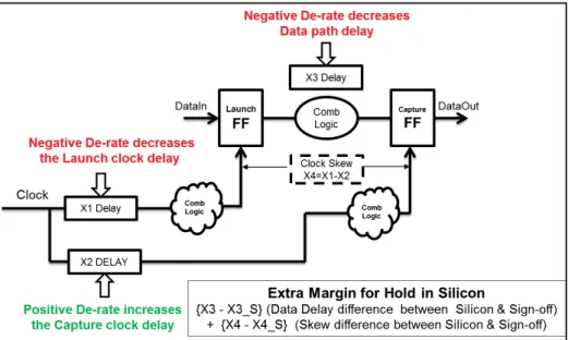
FIGURE 3.1:SIGN-OFF CLOCK DATA DE-RATES ... 42
FIGURE 3.2:CLOCK DATA DE-RATE:BASIC DIAGRAM ... 43
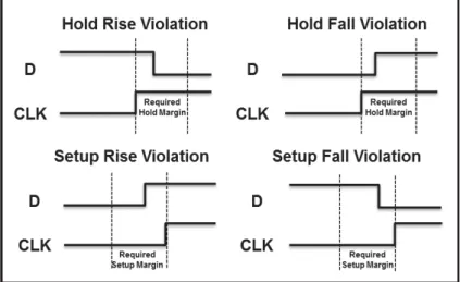
FIGURE 3.3:TIMING DIAGRAMS FOR HOLD RISE/FALL AND SETUP RISE/FALL VIOLATIONS ... 44
FIGURE 3.4:28NM FDSOITEST-CHIP WITH THE CDD BLOCK EMBEDDED AT 7 DIFFERENT LOCATIONS ... 44
FIGURE 3.6:CLOCK DATA DE-RATE:EXTRA MARGIN FOR SETUP IN SILICON ... 46
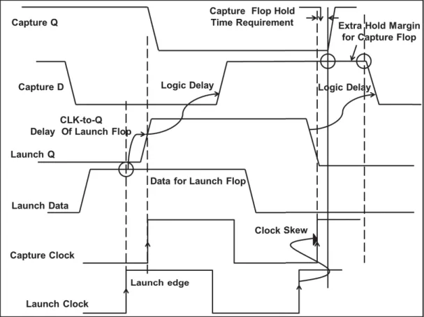
FIGURE3.7:HOLD EXTRA MARGIN WAVEFORMS FOR CAPTURE ... 47
FIGURE 3.8:SETUP EXTRA MARGIN WAVEFORMS FOR CAPTURE ... 47
FIGURE 3.9: NORMALIZED HOLD RISE EXTRA MARGIN ON SILICON DEPICTING WITHIN DIE VARIATIONS & CONSTITUENT COMPONENTS ... 49
FIGURE 3.10: NORMALIZED HOLD FALL EXTRA MARGIN ON SILICON DEPICTING WITHIN DIE VARIATIONS & CONSTITUENT COMPONENTS ... 49
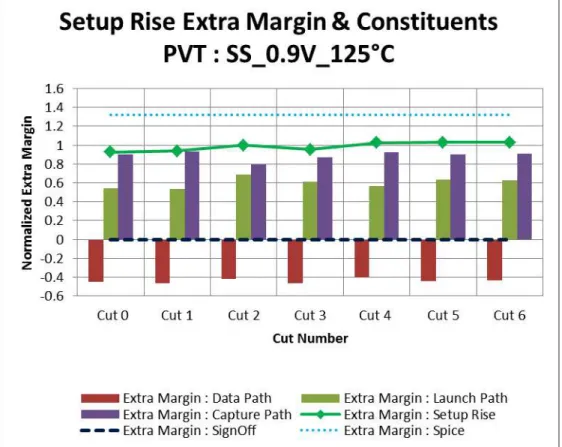
FIGURE 3.11:NORMALIZED SETUP RISE EXTRA MARGIN ON SILICON DEPICTING WITHIN DIE VARIATIONS & CONSTITUENT COMPONENTS ... 50
FIGURE 3.12:NORMALIZED SETUP FALL EXTRA MARGIN ON SILICON DEPICTING WITHIN DIE VARIATIONS & CONSTITUENT COMPONENTS ... 50
FIGURE 4.1: DIFFERENT VOLTAGE MARGINS IN ADDITION TO THE NOMINAL MINIMUM VOLTAGE ... 54
FIGURE 4.2:DIFFERENT IN-SITU DELAY MONITOR SCHEMATICS ... 56
FIGURE 4.3:PRE-ERROR MONITOR SCHEMATIC ... 58
FIGURE 4.4:TIMING DIAGRAM FOR PRE-ERROR MONITOR ... 59
FIGURE 4.5: PATH DELAY HISTOGRAM FOR BCH IP AT DIFFERENT CONDITIONS OF VOLTAGE & PROCESS ... 60
FIGURE 4.6: EXPERIMENTAL TIMING DIAGRAM SHOWING PRE-ERROR FLAGS BEHAVIOR WITH LOWERING VOLTAGE ... 62
FIGURE 4.7: EXPERIMENTAL WARNING FLAG/BCH1 AUTOTEST MAXIMUM FREQUENCIES FOR VARIOUS PVTA CONDITIONS ... 63
FIGURE 4.8:ADAPTIVE VOLTAGE MANAGEMENT FLOWCHART ... 64
FIGURE 4.9: ADAPTIVE WEAROUT MANAGEMENT (A) WITHOUT CONSIDERING AGING EFFECTS AND (B)WITH CONSIDERING AGING EFFECTS ... 65
FIGURE 4.10:DETECTION WINDOW EVOLUTION WITH STRESS TIME ... 66
FIGURE 4.11:MONITORING SYSTEM FAILURE RATE AND POWER REDUCTION FOR VARIOUS DVFS OPERATING CONDITIONS ... 67
FIGURE 4.12: TOTAL POWER SAVINGS WITH RESPECT TO STATIC VOLTAGE MARGIN AT DIFFERENT TEMPERATURES ... 67
FIGURE 5.1: FLOOR PLAN AND OVERVIEW OF TEST-CHIP USED FOR THERMAL
CHARACTERIZATION ... 71
FIGURE 5.2:PATTERN FOR STATIC SELF HEATING MEASUREMENTS ... 72
FIGURE 5.3:PATTERN FOR DYNAMIC SELF HEATING MEASUREMENTS ... 72
FIGURE 5.4:PLL AND THSCLOCK WAVEFORMS ... 74
FIGURE 5.5:MEMORY MANAGEMENT DURING DIGITAL CAPTURE [100] ... 74
FIGURE 5.6:SMARTEST MEMORY OVERFLOW MESSAGE ... 75
FIGURE 5.7:SELECTIVE DIGITAL CAPTURE WAVETABLE ... 76
FIGURE 5.8:EXAMPLE OF A DIGITAL CAPTURE VARIABLE WITH ASSOCIATED PARAMETERS [100] ... 77
FIGURE 5.9: THERMAL CHARACTERIZATION RESULTS FOR STATIC & DYNAMIC CONDITIONS ... 78
FIGURE 6.1: BASIC REPRESENTATION OF POWER SAVINGS THROUGH ADAPTIVE VOLTAGE SCALING ... 83
FIGURE 6.2:APIPBASIC REPRESENTATION ... 84
FIGURE 6.3:GROUPPMM BLOCK DIAGRAM ... 85
FIGURE 6.4:FREQGEN&APIPINTERFACING ... 86
FIGURE 6.5:COMPUTATION EFFORT FOR FULL PVT SIMULATION USING FAST SPICE ... 87
FIGURE 6.6:SIMULATION FLOWS BASED ON CUSTOMSIM &VCSAMS ... 88
FIGURE 6.7: SIMULATION METHODOLOGY OVERVIEW AND RESULTING RUN-TIME IMPROVEMENT ... 89
FIGURE 6.8:FLOWCHART FOR APIPFMAX CHARACTERIZATION ... 91
FIGURE 6.9:FLOWCHART FOR APIPVMIN CHARACTERIZATION ... 93
FIGURE 6.10:NORMALIZED SIMULATION V/S SILICON FMAX COMPARISON AT 125°C ... 95
FIGURE 6.11: NORMALIZED SIMULATION V/S SILICON LEAKAGE CURRENT COMPARISON AT 125°C ... 95
FIGURE 6.12: NORMALIZED SIMULATION V/S SILICON DYNAMIC_POWER/MHZ COMPARISON AT 125°C ... 96
FIGURE 6.13:NORMALIZED SILICON RESULTS FOR POWER SAVING THROUGH AVS AT 30°C ... 96 FIGURE 6.14: NORMALIZED SILICON RESULTS FOR DYNAMIC POWER SAVING THROUGH
AVS FOR FF CORNER CHIP AT 30°C ... 97
FIGURE 7.1:FDSOIWELL ARCHITECTURES [104] ... 101
FIGURE 7.2:STATIC CURRENT VS.FREQUENCY TREND FROM 0.5 TO 1.3V OF VDD[104] 101
FIGURE 7.3:QUASI-FO4CRITICAL PATH ... 102
FIGURE 7.4:POLY BIAS CELLS LEAKAGE VS QUASI-FO4 CRITICAL PATH FREQUENCY ... 102
FIGURE 7.5:10TRANSISTOR ULVBITCELL ... 103
FIGURE 7.6: COMPARISON OF LEAKAGE BETWEEN ULV 10T DUAL WELL (DW) AND
SINGLE WELL (SW) BITCELLS ... 104
FIGURE 7.7:SPARCV832B LEON3 MICROPROCESSOR SYSTEM &FDSOI28NM RETICLE PICTURE ... 104
LIST OF TABLES
TABLE 2.1: COMPARISON OF PEAK POWER AWARE AND PEAK POWER UNAWARE
APPROACHES ... 31
TABLE 2.2:NORMALIZED PROCESS VARIATION VALUES ACROSS PVTPOINTS ... 33
TABLE 2.3: NORMALIZED PERCENTAGE OF WITHIN DIE VARIATION WITH RESPECT TO PROCESS CORNERS... 33
TABLE 2.4: NORMALIZED PERCENTAGE OF WITHIN DIE VARIATION WITH RESPECT TO VOLTAGE ... 34
TABLE 2.5: NORMALIZED PERCENTAGE OF WITHIN DIE VARIATION WITH RESPECT TO TEMPERATURE ... 34
TABLE 2.6:NORMALIZED CAD AND SILICON SPREAD VALUES ACROSS PVTPOINTS ... 36
TABLE 3.1:CLOCK &DATA DELAY POSITIVE DIRECTIONS IN THE GRAPH ... 48
TABLE 4.1:IMPLEMENTATION RESULTS OF BCHIP WITH IN-SITU MONITORS ... 61
TABLE 7.1:MICROPROCESSOR PERFORMANCE COMPARISON ... 106
TABLE 7.2:COMPARISON OF EXECUTION ENERGY WITH AND WITHOUT CACHE ACTIVATION ... 107
LIST OF ABBREVIATIONS
ABB Adaptive Body Bias
APIP Area and Power IP
ASIC Application Specific Integrated Circuit
ATE Automatic Test Equipment
ATPG Automatic Test Pattern Generation
AVM Adaptive Voltage Management
AVS Adaptive Voltage Scaling
AWM Adaptive Wearout Management
BCH Bose Ray-Choudhary and Hocquenghem
BOX Buried Oxide
CAD Computer Aided Design
CDD Clock Data Derate
CMOS Complementary Metal Oxide Semiconductor
CPR Critical Path Replica
CUT Circuit Under Test
DFT Design For Test
DVFS Dynamic Voltage and Frequency Scaling
FDSOI Fully Depleted Silicon On Insulator
FMAX Maximum Frequency
FMIN Minimum Frequency
IC Integrated Circuit
IOT Internet Of Things
IP Intellectual Property ISM In-Situ Monitor
ITRS International Technology Roadmap for Semiconductors
LOC Launch Off Capture
LOS Launch Off Shift
MTF Mean Time to Failure
PRBS Pseudo Random Binary Sequence
PV Process Variation
PVT Process Voltage Temperature
PVTA Process Voltage Temperature Aging
SE Scan Enable
SM Sequencer Memory
SOC System On Chip
SPARC Scalable Processor Architecture
STA Static Timing Analysis
UTBB Ultra Thin Body and Buried Oxide
VLSI Very Large Scale Integration
VM Vector Memory
VMAX Maximum Voltage
INTRODUCTION
“Nearly all men can stand adversity, but if you want to test a man's character, give him power.” Abraham Lincoln
The ever-increasing advances in semiconductor technology evolution continue to open new avenues for research in the domains of digital circuit design and test. Designing and manufacturing smaller, faster, cheaper and low-power devices are some of the main challenges for the semiconductor industry. The incessant increase in density and the corresponding decrease in feature sizes of Integrated Circuits as evinced by Moore’s Law [1] have been a driving force in the progress of the industry for the past few decades. However, scaling of CMOS structures into the nanometer domain has posed new challenges to the physical design and reliability of circuits. The reasons for this are manifold [2, 22-24]. Firstly, manufacturing structures much smaller than the wavelength of light used in modern lithography are difficult to fabricate and can be practically done only with certain coarse limits. Similarly, it is difficult to control the doping concentration for transistors in the nanometer range. Further, the structures are located closer to each other with every technology node, resulting in even the smallest of impurities or metal silvers being able to create shorts or other defects. Lastly, as the number of transistors, wires, contacts and vias on a single chip increase, the probability of one or more of them being faulty increases. These limitations have resulted in increasing the probability of defects in advanced technology nodes.
A circuit defect may lead to a fault causing an error that can result in a system failure. Manufacturing defects are physical defects introduced during manufacturing that cause the circuit to fail to function properly. The diversity of defects makes it difficult to generate meaningful tests maximizing the defect coverage. Fault models which are gate-level representation of physical defects are necessary for generating and evaluating a set of test patterns. Generally, a good fault model should accurately reflect the behavior of the physical defects and should be computationally efficient in terms of the time required for fault simulation and test generation. Many fault models have been proposed, but unfortunately, no single fault model accurately reflects the behavior of all
possible defects that can occur. As a result, a combination of different fault models is often used in the generation and evaluation of test patterns. Some well-known and commonly used fault models for modern VLSI test, developed to describe different kinds of physical defects, include the stuck-at, bridging and delay fault models [19].
As many faults are not visible at the design phase, they can only be handled by discarding faulty chips after manufacturing and testing them. Since the faults become visible only post-fabrication, circuits need to be tested with patterns that can detect the presence of any defects. This in turn necessitates the need for having effective test architectures and methodologies for efficiently capturing all modelled faults while maintaining ease of application. Different test methodologies like parametric, functional, structural and delay testing are combined together to maximize the fault detection. Parametric testing is typically used to check the electrical properties of the device and can be used to characterize any potential systematic issues with the process node. These tests may not check any functionality of the device but can find gross shorts, opens, leakage issues, or current drive problems. Functional testing is commonly used for design verification to check if the output responses are inline with expected values according to design specifications. However it is considered time consuming and expensive due to the exhaustive nature of applying test patterns to cover each known reachable functional state. Structural tests deal with observing the state of internal signals at the primary outputs of a circuit. Unlike functional testing, structural tests do not require enumeration of all functional states to test the design, so test volumes are not as large. Delay tests are used to detect the presence of very rise or very slow-to-fall switching transitions and verify that a design operates correctly at the specified clock speed.
The importance of testing cannot be overstated as it is required at different stages of the semiconductor lifecycle from the qualification of new technology nodes to diagnosis of in-field failures. The optimal test solution for any circuit must take into account a wide variety of different factors like fault coverage, test cost and time, capability of available test equipment, reliability requirement of end-user application, etc. Often times these different factors aren’t complementary to each other and require intelligent trade-offs to be made on a case to case basis. This eliminates the possibility of having a global test solution for a wide variety of circuit designs and applications. Hence custom test solutions and methodologies are required and developed which are specific to the circuit design and application. In this context differentiated test solutions
for different problems at various levels of circuit complexity ranging from simple standard cells to complex microprocessors are presented as part of this thesis. The main contributions are divided into six distinct chapters in this manuscript. It is pertinent to note that the organization of the chapters follows the level of circuit complexity involved, from basic standard cells to complex microprocessors. The content of each chapter is briefly summarized below:
· Chapter 1 details the context and objectives of the presented research work. It starts with a discussion on the trends in semiconductor technology scaling and the resultant challenges that have emerged. Thereafter the Fully Depleted Silicon On Insulator (FDSOI) technology node and basic concepts related to semiconductor test are discussed. The final part of the chapter enumerates the main objectives of this thesis.
· Chapter 2 presents a configurable circuit and an associated power-aware at-speed test methodology for the purpose of qualifying basic standard cells and IP structures to detect the presence of small delay defects. The relevant silicon results and analysis validate the proposed power-aware test methodology for qualification and characterization of IPs and provide deeper insights for process improvements.
· Chapter 3 presents a design and methodology for accurate characterization of setup and hold margins of sequential elements in silicon while taking into account effects of Process Variations. The test results provide deeper insights into sources of extra timing margins available on silicon. This in turn, enables accurate guard banding by preventing optimism and reducing unnecessary pessimism in the timing margins provided during sign-off.
· Chapter 4 shows the fundamental elements towards an Adaptive Wearout Management (AWM) control loop for the dynamic supply voltage regulation of digital circuits. Firstly a new generation of in-situ monitors which generate warning flags to prevent circuit failure under nominal conditions have been explained. A voltage management control loop to efficiently tackle all voltage margins over a large range of DVFS operating conditions and temperatures has been implemented. The relevant experimental silicon results related to timing windows and power savings have been provided.
· Chapter 5 elucidates a methodology for thermal characterization under dynamic workloads using embedded digital sensors. Firstly the design of the test-chip used is explained and thereafter the test patterns and test methodology employed are elaborated upon. In particular, the methodology required for managing high volume of data generated during such tests is elaborated upon. Analyses of the on-chip thermal results provide useful insights for test-chip design requirements related to thermal measurements.
· Chapter 6 presents the full silicon level electrical characterization correlation of the simulation done using a novel method based upon existing CAD tools and a mixed mode approach, on a representative digital design. Thus enabling complete Process-Voltage-Temperature (PVT) characterization on the portion of the design for which Adaptive Voltage Scaling (AVS) is defined. The correlation of silicon results with the ones obtained via the simulation flow provide designers with deeper insights into the gains with AVS from within the simulation environment.
· Chapter 7 presents the design and performance metrics of a single-supply SPARC 32bit V8 microprocessor designed with Ultra Low Voltage (ULV) adapted standard cells and memories, aiming at low energy operation and stand by power. A comparative analysis with similar implementations has been provided highlighting the performance gain and power savings that are achieved by the presented design methodology and implementation technology. Wafer-level tests throw light on the operating range and energy savings achieved by the ULV adapted microprocessor.
· Chapter 8 concludes the manuscript by summarizing the results of this thesis and presenting some future perspectives.
1 C
ONTEXT AND
T
HESIS
O
BJECTIVES
“The best way to have a good idea is to have a lot of ideas.” Linus Pauling
1.1 Semiconductor Technology Evolution
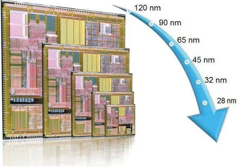
Technology scaling allows realization of increasingly complex systems on a single chip. The steady growth of the global semiconductor industry over the past few decades has been driven by the demand for enhancing performance and functionality at reduced cost. This growth has been primarily facilitated by the continuous evolution of semiconductor manufacturing technology. Following the so-called Moore’s law [1], the scale of ICs has doubled every 18 months. A simple example of this trend is the progression from Small Scale Integration (SSI) to Very Large Scale Integration (VLSI) devices. In the 1980s, the term VLSI was used for chips having more than 100,000 transistors and has continued to be used over time to refer to chips with millions and now hundreds of millions of transistors. In 1986, the first megabit Random Access Memory (RAM) contained more than 1 million transistors. Microprocessors produced in 1994 contained more than 3 million transistors. VLSI devices with many millions of transistors are commonly used in today’s computers and electronic appliances. This is a direct result of the steadily decreasing dimensions, referred to as feature size, of the transistors and interconnecting wires from tens of microns to tens of nanometers, with current submicron technologies based on feature sizes of just a few nanometers. Transistors are scaled in each successive technology node to increase their speed, improve packing density, decrease their power consumption and reduce cost. The reduction in feature size has also resulted in increased operating frequencies with current commercially available microprocessors operating in the gigahertz range. Thus, semiconductor technology scaling optimizes circuit performance and power consumption, and allows realization of more and more complex systems [2]. Figure 1.1 representatively depicts the shrink in silicon area required for fabricating the same circuit in successively smaller technology nodes.
1.2 Challenges in Advanced Technology Nodes
While offering many advantages, technological trends into the nanometer regime have led to a host of challenges. The sources that affect the integrity and reliability of modern circuits and systems are wide spread including manufacturing
Figure 1.1: Effects of scaling with successive technology nodes
process variations, manufacturing defects, wear-out and interference. In this section we discuss some of the major issues that have emerged with technology scaling.
1.2.1 Variability
Variability of transistor characteristics due to variations in Process, Voltage and Temperature (PVT) have always been an issue in integrated circuit design [3]. PVT variations may prevent the circuit from achieving the required performance even in the case of fault-free fabrication. As device scaling enters into the nano-metric regime the effects of PVT variations are becoming excessively pronounced. Manufacturing process variations are increased due to the lack of precise control on fabrication processes at small-feature technologies. They cause deviation of transistor characteristics and the resulting wide distribution leads to lower parametric yield [4]. Supply voltage scaling brings it close to or even below the transistor threshold voltage (Vth) to achieve
significant gains in energy efficiency. Once the supply voltage is lower than Vth the
delay shows an exponential dependence on the supply voltage, and therefore the magnitude of supply voltage shifts can have a significant impact on circuit delay [5, 6]. Scaling also gives rise to chip power densities and inadequate heat sinking cause hot spots to appear. These fluctuations of ambient temperatures alter the timing characteristics of circuits [7]. A conventional approach to deal with the problem of variability is to introduce large voltage and frequency guard-bands during sign-off which considerably impacts the power consumption and performance, cannot respond to
rapid environmental changes [8] and implies a sharp increase in chip cost. Effectively dealing with variability to maintain or improve the high performance and energy efficient systems while satisfying the required standards for reliability is becoming increasingly challenging with the scaling of technology [9].
1.2.2 Manufacturing Defects
Semiconductor manufacturing processes may induce permanent defects in a chip during one or more of the process steps involving implantation, etching, deposition, cleaning and lithography due to imperfections. The device miniaturization is making advanced technology nodes increasingly vulnerable to these manufacturing irregularities. It is important that the testing be as thorough as possible to uncover defective chips before they are shipped out [10]. However, according to past microprocessor data, the die size remains relatively constant [11], whereas the number of transistors per chip double every 2 to 3 years. This means that defect densities continue to increase. Moreover technology scaling and increasing complexity give rise to defects which are more subtle and difficult to detect [12, 13]. All these factors when combined with aggressive time-to-market objectives cause test escapes and raise reliability concerns.
1.2.3 Wear-out
Although the area scaling has had an exponential rate, the supply voltage (Vdd)
scaling has been quite slow. The two main reasons for slow Vdd scaling are to keep up
with the competitive frequency growth and to retain the basic noise immunity and cell stability [14]. Hence the dissimilar area and supply voltage scaling rates result in high power densities and elevated temperatures. The well-known wear-out failure mechanisms namely Time-Dependent Dielectric Breakdown (TDDB), Electromigration and thermal stress are all adversely affected by increase in temperature. These age-related hard errors that appear in-field after a certain period of use are major factors impairing the life-time reliability of modern microprocessors [15] used in data centers and space equipment. These applications demand high throughput and better lifetime reliability. However, these wear-out failures limit their useful lifetime and performance.
1.2.4 Interference
Beyond manufacturing defects and wear-out related permanent faults, integrated systems of recent years are more susceptible to temporary effects like transient or intermittent faults. Smaller geometries increase coupling capacitances and as a result, cross-capacitance between wires in nanometer interconnect structures has turned out to be the dominant component of total net capacitance. High interconnect coupling leads to increase in circuit delay and crosstalk noise. Therefore, reducing of interconnect coupling capacitance is an important task in the view of both circuit noise and timing optimization. [16 - 18]
1.3 FDSOI Technology Node
Figure 1.2: Schematic layout of Bulk and FDSOI Transistors
To build better devices, the size of the transistors must be reduced while increasing performance and reducing power consumption. FDSOI or Fully Depleted Silicon on Insulator [38] is an advanced technology node that delivers these benefits by building transistors that are faster, cooler and simpler. In FDSOI, the innovation lies in inserting a thin layer of Insulator called the Buried Oxide (BOX) positioned just below the channel and eliminating the need to add dopants to the channel, thus making it fully depleted. Another key feature is that the silicon on oxide layer is very thin together with the ultra thin body layer. Together this is referred to as the Ultra Thin Body and Buried Oxide (UTBB). On the same technology node, the FDSOI transistors have a shorter effective channel as compared to a bulk silicon transistor. This reduces the effective
time required by electrons to travel from the source to the drain, leading to faster transistor. Figure 1.2 shows the schematics of Bulk and FDSOI Transistors.
As the transistor shrinks, the length of the gate is reduced and the control the gate exercises over the channel region is also reduced thereby lowering the transistor performance. Some unwanted leakage current flows even when the transistor is turned off and represents a growing proportion of power consumption with each new technology node. For FDSOI transistors, the insulator layer effectively confines the electrons from the source to the drain thereby drastically reducing the leakage currents from the channel to the substrate. An FDSOI chip is able to run at a lower voltage due to the reduced margins added for process variability which also makes it cooler with lower power consumption. To summarize, FDSOI transistors operate at lower power at equivalent frequency as compared to their bulk counterparts.
The fabrication of all designs and their associated silicon validation results presented within the scope of this thesis employ the 28nm FDSOI unless stated otherwise.
1.4 Testing Overview
Figure 1.3: Basic testing approach
The reduction in feature size increases the probability that a manufacturing defect in the IC will result in a faulty chip. A very small defect can easily result in a faulty transistor or interconnecting wire when the feature size is less than 100 nm.
Furthermore, it takes only one faulty transistor or wire to make the entire chip fail to function properly or at the required operating frequency. Yet, defects created during the manufacturing process are unavoidable, and as a result, some number of ICs are expected to be faulty. Therefore, testing is required to guarantee fault-free products, regardless of whether the product is a VLSI device or an electronic system composed of many VLSI devices. The goal of manufacturing test is to detect any defect that occurs in the fabricated circuits. Ideally, we can differentiate faulty circuits and fault-free circuits after the manufacturing test. Figure 1.3 illustrates the basic principle of chip testing [2] wherein test vectors are applied to inputs of the Circuit-Under-Test (CUT), and responses are collected and compared with expected values. If the responses match, the circuit is considered good. Otherwise, it is considered bad. The Automatic Test Equipment (ATE) is used to test chips. It is obvious that the test quality depends upon the thoroughness of the test vectors. However, the test quality and test cost are interdependent. A large number of test vectors/patterns may result in a good test quality, but it will increase the test time and test cost at the same time. It is also necessary to test components at various stages during the manufacturing process. Testing and diagnosis of VLSI systems can be broadly classified into four types depending on the specific purpose it accomplishes and the current phase of production (from fabrication to shipment) for the circuit under test [19]. In the following subsections, four types of test methods are briefly covered in the order they are conducted during the design and manufacturing processes.
1.4.1 Characterization Test
Also known as design debug or verification testing, this form of testing is performed on a new design before it is sent to production [19]. The main objective of characterization test is to verify that the design is correct and the device will meet all specifications. Comprehensive AC and DC measurements are made during this test process. The requirement for thoroughness during this testing phase may often lead to probing of internal nodes of a chip, not performed as part of any other test process. Generally, devices are tested for the worst case because it is easier to evaluate than average cases and devices passing this test usually work for any other conditions.
1.4.2 Production Test
Every fabricated chip is subjected to production tests, which are less comprehensive than characterization tests yet they must enforce the quality requirements by determining whether the device meets specifications. It may not be possible to cover all possible functions and data patterns, but production tests must have a high coverage of modelled faults. Since every device must be tested before being packaged, test application time is of great importance. Production test should be as brief as possible and is usually different from characterization tests.
1.4.3 Burn-in Test
Figure 1.4: Bathtub curve showing the rate of failure of integrated circuits at different phases of life
All devices that pass production tests are not identical. When put to actual use, some will fail very quickly whereas others will function for a long time. Burn in tests screen for long-term reliability of devices by either continuous or periodic testing over a period, usually under nonrated conditions. Rate of failure of integrated circuits at different phases of life follows a bathtub curve [20] as shown in Figure 1.4. Correlation studies show that the occurrence of potential failures can be accelerated at elevated temperatures [21]. Two types of failures are isolated by burn-in:
1. Infant mortality failures, often caused by a combination of sensitive design and process variation, and may be screened out by a short-term burn-in (10–30 h) in a normal or slightly accelerated working environment, and
2. Freak failures, that is, devices having the same failure mechanisms as the reliable devices, require long burn-in time (100–1000 h) in an accelerated environment.
In practice, a manufacturer must balance economic considerations against the device reliability. In any case, the elimination of infant mortality failures is considered essential for most applications [19].
1.4.4 Incoming Inspection
System manufacturers perform incoming inspection (also called quality assurance) on purchased devices before integrating them into the system. Depending upon the context, this testing can be either similar to production testing, or more comprehensive than production testing, or even tuned to the specific systems application. The most important purpose of this testing, performed at the vendor site, is to avoid placing a defective device in a system assembly where the cost of diagnosis may far exceed the cost of incoming inspection.
The development of new technology platforms is done through the validation of various test chips, which fulfil the fundamental requirement of determining the silicon parameters of IP’s (functionality, timing, power, etc.) before they can be used in a real System-on-Chip. Therefore, while qualifying new technology nodes, it is essential to ensure that the silicon performance of test circuits is within acceptable limits. Furthermore, accurate diagnosis and understanding of the sources of deviation from expected behaviour is essential for improving the yield and performance of a given technology node.
1.5 Research Objectives
The work of this thesis is focused on the development of efficient test methodologies that aid in the accurate detection and resolution of issues that may arise due to variability, manufacturing defects, wear-out or interference. The intent is to
tackle a wide spectrum of these challenges from a test perspective to ensure that the availability of effective test solutions does not become a bottleneck in the path towards further scaling. To this end, special emphasis is laid on capturing faults and understanding deviation from expected behavior during the process development phase itself. The goal is to address the great need and scope to improve and optimize existing test structures and methodologies with regards to test time, silicon area occupied by test structures and the ability to analyze the impact of deep submicron effects. Additionally the aim is to develop advanced, modular and agile test methodologies that address the advances and innovations introduced in the myriad domains of electronic design, reliability management, manufacturing process improvements etc. The main objectives of the thesis are briefly listed below:
· Develop a power-aware at-speed test methodology for the purpose of qualifying basic standard cells / complex IP structures and detect the presence of small delay defects at an early phase of technology development.
· Accurately characterize setup and hold margins of sequential elements in silicon while taking into account effects of Process Variations. The test results should provide deeper insights into the constituent components of extra timing margins available on silicon. This in turn should enable accurate guard banding by preventing optimism and reducing unnecessary pessimism in the timing margins added during sign-off.
· Validate and characterize the functionality of a new generation of pre-error warning monitors. Implement an Adaptive Wearout Management (AWM) control loop for dynamic supply voltage regulation of digital circuits using the warning flags generated by the pre-error monitors. Analyse the silicon results to quantify the reliability benefits and power savings that are accrued from the implemented AWM strategy.
· Develop a test methodology for thermal characterization under dynamic workloads using embedded digital sensors. In particular, the methodology should be capable of capturing the thermal gradient across small time intervals and also be efficient in managing the resultant high volume of generated data. Analyses of the on-chip thermal results should provide useful insights into dynamic self-heating on silicon and should also show directions for future test-chip design requirements related to thermal measurements.
· Implement the full silicon level electrical characterization correlation of the simulation done using a novel method based upon existing CAD tools and a mixed mode approach, on a representative digital design. The correlation of silicon results with the ones obtained via the simulation flow should provide designers with deeper insights into the gains achieved using Adaptive Voltage Scaling from within the simulation environment.
· Evaluate the electrical performance metrics of a single-supply SPARC 32bit V8 microprocessor designed with Ultra Low Voltage (ULV) adapted standard cells and memories, aiming at low energy operation and stand by power. Wafer-level tests should throw light on the operating range and energy savings achieved by the ULV adapted microprocessor. Further perform a comparative analysis with similar implementations to understand the performance gain and power savings that are achieved by the design methodology and implementation technology.
2 A
N
E
FFECTIVE
P
OWER
-A
WARE
A
T
-S
PEED
T
EST
M
ETHODOLOGY FOR
IP
Q
UALIFICATION AND
C
HARACTERIZATION
“The real voyage of discovery consists not in seeking new landscapes but in having new eyes.”
Marcel Proust
Abstract: Advanced nanometer technologies have led to a drastic increase in operational
frequencies resulting in the performance of circuits becoming increasingly vulnerable to timing variations. The increasing process spread in advanced nanometer nodes poses considerable challenges in predicting post-fabrication silicon performance from timing models. Thus, there is a great need to qualify basic building structures on silicon in terms of critical parameters before they could be integrated within a complex System-on-Chip (SoC). This chapter presents a configurable circuit and an associated power-aware at-speed test methodology for the purpose of qualifying basic standard cells and complex IP structures to detect the presence of small delay defects. The circuit design has been embedded within test-chips used for the development of the 28nm Fully Depleted Silicon On Insulator (FDSOI) technology node. The relevant silicon results and analysis validate the proposed power-aware at-speed test methodology for qualification and characterization of IPs and provide deeper insights for process improvements.
2.1 Introduction
Consequent application of reusable components (IP: Intellectual Property) is indispensable to enhance productivity in system design. IP qualification is a process to measure and evaluate the specific attributes of IP cores. Its goal is to ensure that the required quality & reliability of IP blocks is achieved and that all design constraints are met. IP qualification offers IP providers and integrators with measurable quality characteristics that allow making design decisions based upon quantifiable metrics of performance and reliability [25-27]. The development of new technology platforms is done through the silicon qualification of basic building structures/gates embedded within test-chips, which ensure greater controllability and observability of the Circuit Under Test (CUT). While qualifying new technology nodes, it is essential to understand the silicon performance of CUTs and ensure that it is within acceptable limits. Test-Chips fulfil the fundamental requirement of determining silicon parameters of IP’s (functionality, timing, power, etc.) before they can be integrated in a real SoC design. Having modular design architectures for test, effective test methodologies, efficient diagnosis of defects and the ability to accurately characterize the impact of Process Variations (PV) [28, 29] is essential to the IP Qualification process.
From a post-silicon test point of view, the physical phenomenon observed in deep sub-micron nodes give rise to new defects and immensely complicate the task of timing analysis and path selection for testing and grading the final chips. IC manufacturing test is continually evolving, with an increased emphasis on at-speed testing to maintain test quality for larger, more complex chips and new fabrication processes. At-speed testing is crucial for ensuring product quality from the timing performance point of view and maintaining the reliability level of chips delivered to customers after testing. At-speed testing is now the industry norm as many timing related defects go undetected by ATPG patterns generated using the classical stuck-at and bridging fault models [30, 31]. Further, power consumption during test is significantly higher than during normal functional mode [19, 32-35]. The reason is that test patterns tend to activate switching on a large number of nodes while a typical functional mode only activates a small portion of the design at any given time instance. Also successive functional input vectors applied to a given circuit during system mode have significant correlation, while the correlation between consecutive test patterns can be very low [36]. The excessive power consumption can result in parts being damaged
during test, or in preventing good parts from passing test, leading to yield loss. This necessitates the need to develop power-aware test methodologies. In order to have proper characterization in terms of timing it becomes inevitable to evaluate the impact of aging degradation too through burn-in tests. Stress tests such as high voltage tests and burn-in tests are often used to perform accelerated testing in order to detect infant moralities and screen weak parts [37]. Furthermore, accurate diagnosis of the sources of defects & deviations from expected behaviour is essential for improving the yield and performance of a given technology.
In this context, this chapter presents a circuit design which may be embedded within test-chips and an effective test methodology that enables the characterization of basic standard cells and/or complex IP structures. This helps in detecting Small Delay Defects (SDD) at an early phase of technology development. The circuit design & test methodology have been optimized for low power consumption & used for the development of the 28nm FDSOI technology node [38]. The associated relevant results and analysis provide deeper insights into the speed limitations, reliability and defectivity of the said technology node. Furthermore, silicon results help in the diagnosis of captured defects and in qualifying the standard cell library with respect to multiple Process-Voltage-Temperature (PVT) configurations.
2.2 Background and Motivations
Performance verification in the presence of PV is difficult to perform because the critical path is no longer unique. Different paths become frequency limiting in different process corners. In advanced nanometer manufacturing, systematic delays owing to unpredictable process changes have assumed a greater share of customer fails than catastrophic defects [39]. Conventional ASIC design methodology uses pre-characterized standard cells to optimize the design as per specifications. During the process development phase it is necessary to complement pre-silicon analysis with post-silicon timing and power characterization on fabricated devices. Characterization results are used to identify outliers, understand the impact of PV and improve the design before ramp and production [40]. Accurate timing characterization of standard cells as well as
complex IPs is required for power and performance optimization of designs which embed them.
It has been observed that the presence of random defects can affect circuit performance with very slow-to-rise or very slow-to-fall switching transitions [41]. Such defects can cause an increase in the delay of paths going through circuits. A device fails to operate at the rated speed if it contains a delay defect that creates a path delay higher than the maximum allowed path delay [42]. The different fault models for generating test patterns for delay defect detection are the transition delay model, the path delay fault model and the SDD fault model. In the transition fault model [43], a gate net has a slow-to-rise and a slow-to-fall fault associated with it while the path delay fault model [44] targets the cumulative delay through the entire set of gates in a pre-defined path. Moreover, the path delay fault model not only takes into account the cumulative delay through the entire list of gates in a pre-defined path, but it can also take into account localized delay defects. Depending on how delay faults are tested in scan design environment, there are two transition delay fault pattern generation approaches, namely the Launch-Off-Shift (LOS) and Launch-Off-Capture (LOC) schemes [30, 45]. Application of at-speed tests for detecting delay faults in synchronous sequential circuits is usually done using scan-based structural tests generated by an Automatic Test Pattern Generator (ATPG). Timing-aware ATPGs require long CPU run time for pattern generation and fault simulation, and also result in a significantly large pattern count [46]. In [47], a variation aware method based on statistical timing to select critical paths for structural test is discussed wherein path delays are projected into different process corners using their linear delay function forms. The work of [48] has explored improving transition fault pattern quality through at-speed diagnosis to automatically identify the failing paths and locate the root cause of failure. The premise is that complete timing information is unavailable during ATPG and it may be possible that some of the at-speed patterns may activate paths which are not required to meet system speed (for e.g. non-functional paths), and these patterns may fail during production test.
Power inducing over-test occurs when fully-functional chips fail during testing because of excessive heat and/or Power Supply Noise caused by test patterns with excessive switching activity and is rapidly becoming one of the most serious problems in scan testing, especially for low-power, high-speed, and deep-submicron integrated circuits [49, 50]. This is particularly aggravated during burn-in testing which can lead to significant power variations within the die [51]. Since power consumption increases
significantly with elevated temperature and voltage, the execution of burn-in tests can be limited by the allowed power dissipation budget [52]. For scan-based tests, power is divided into shift-power and capture-power. Shift-power is the power consumed during the process of simultaneously serially loading the test stimulus and unloading the previous test response whereas capture-power is the power consumed during one or more capture clock cycles. Generally, test power problems are classified as peak power issue which is highest permissible value of power at any given instant and average power issue which is total distribution of power over a time period [53]. Test power reduction can be addressed at various stages of test generation for logic circuits, by employing low-power ATPG, low-power test compaction, low-power X-filling, and low-power test vector ordering [54]. The most significant advantage of reducing test power through low-power test generation is that this approach causes neither circuit overhead nor performance degradation. Power-aware Design-for-Test (DfT) techniques allow for controlling the power consumption and reduce the overall energy consumed during test. Clock gating can be employed to reduce test power without impacting fault coverage. Techniques such as segmentation, clustering and ordering of scan cells reduce the power consumption, and improve the effectiveness of power reduction techniques such as test planning and power-aware test generation [54]. A common method to reduce the excess switching activity during shifting is to split the scan path into several segments. Shifting is then done one segment after the other [55]. The segments not currently active are not clocked and do not contribute to shift power. Staggered clocking or skewed clocking is a technique used in low-power design where segmented parts of a design are clocked in an alternating fashion to reduce the simultaneous switching activity and thereby the peak power during test [56, 57].
The work of this chapter focuses on the detection of timing related defects at the standard cell level during the process development phase. The presented power-aware modular design structure and test methodology allow for the reduction of capture power during at-speed tests. The proposed framework and methodology simplify the procedure for fault diagnosis and outlier localization using functional at-speed patterns. The associated results and analysis help in further understanding the effects of PV across multiple corners on timing related defects and design margins.
2.3 Circuit Design Architecture and Implementation
Figure 2.1: Basic structure of a Tile
The primary intent of the design is to enable the qualification of basic digital structures, gates or IPs by accurately determining their operational parameters and characteristics at high frequencies. In terms of physical implementation, a bottom-up approach has been used by implementing the basic building structure of the design and then using it as a hard-macro for further implementation. This basic building structure referred to as a Tile and is shown in Figure 2.1.
A tile consists of N different standard cells or complex IP structures between launch and capture flops. The capture flop is referred to as the Scan Flop as it forms part of the output scan chain. The Circuit Under Test (CUT) refers to a single standard cell / IP as shown in Figure 2.1. CUTs embedded within a tile for the purpose of qualification differ in terms of geometry and characteristics such as layout, orientation etc. A CUT is activated and tested by either a rising or falling transition. A NX1 multiplexer is used to select & observe the output of any CUT within the tile, which is then captured into the scan flop. Scan flops of multiple tiles are stitched together to facilitate the shifting out of the CUT’s capture response, such that it is observable on the top-level pad of the test-chip. The excitation stimuli may be either generated on-chip or loaded externally depending on the mode in which we are the structure is operated. For retaining observability in case of any faults within the scan chain, redundancy has been added using a Bypass Mux structure. Launch and capture flops as well as multiplexers employed within the tile have higher reliability as compared to embedded CUTs i.e. they have been qualified earlier or if the tile is used for the qualification of an entirely new technology node, these cells employ a relatively relaxed geometrical layout. A tile
can be clocked dynamically by either using the slow tester clock or a fast clock generated using an on-chip PLL.
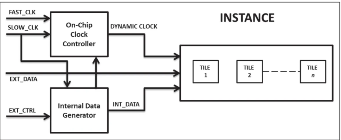
Figure 2.2: Illustration of instance interfacing with controlling circuitry
For having a large population of tiles to help in better understanding the properties of fabricated devices while maintaining ease of design, each tile is replicated several times within an instance as shown in Figure 2.2. Each instance is then interfaced with an internal on-chip data generator and an On-Chip Clocking (OCC) mechanism. The internal data generator is a Linear Feedback Shift Register which provides rising and falling transitions. Having an on-chip data generator provides the possibility to easily test an instance when it is not possible to apply stimuli from top-level pads of the test-chip. Such a requirement may be mandatory for Burn-In testing where limited number of pins may be available on the Burn-In board due to hardware limitations of the oven equipment.
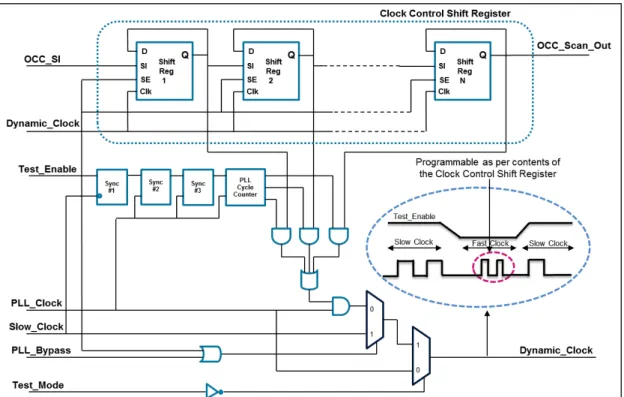
The on-chip clock controller shown in Figure 2.3 is used to generate at-speed clock pulses. The OCC is a complex multiplexer with synchronization circuitry, which selects between at-speed (PLL) clock and slow clock depending on the status of the Test_Enable signal. The length of the Clock Shift Register is easily configurable & is programmed to generate the required number of fast clock pulses during capture mode, i.e. Test_Enable = 0 & Test_Mode = 1. During capture, the Test_Enable signal is latched internally at the negative edge of the Slow_Clk which enables the generation of fast clock pulses depending on the contents of the clock shift register. The configurable clock shift register provides flexibility to adjust the arrival time of the at-speed pulses after the Test_Enable signal goes low. This forms the basis of the proposed architecture for peak power reduction.
Figure 2.3: On-Chip Clock Controller
Figure 2.4: IP Qualification Block
As shown in Figure 2.4, an instance is further replicated inside a Block with the goal of increasing the cell population. For the test case under consideration, a single block contains 5 instances with 100 tiles (Instances 1 - 5) and 3 instances having 50 tiles (Instances 6 - 8). Each tile embeds within itself 128 CUTs. This leads to a population of about 80k CUTs within a single block. However, this configuration can be easily modified to suit specific requirements. Having multiple instances embedded within a single test-chip allows studying the impact of within die variations on performance. This architecture and implementation flow not only enables IP qualification but also helps us to reuse small portion of the structure multiple times resulting in reduction of overall development cycle of the test-chip. The modular design allows sharing resources and increasing area utilization efficiency for different tiles and instances. The presented circuit design is capable of being clocked in the GHz range and occupies a chip area of 1.18 mm2 when implemented in the 28nm FDSOI technology. Figure 2.5 shows the floor-plan of the test-chip, instance and tile respectively.
2.4 Test Methodology
In this section, firstly the application of power-aware at-speed patterns employed for testing tiles within the test-chip design have been explained with the aid of timing diagrams. Thereafter, the test flow used for qualifying the CUTs embedded into the test-chip is explained.
2.4.1 Test Patterns
Figure 2.6 shows the timing diagram when a tile is clocked during at-speed test. The LOC approach is used for this implementation permitting the scan chain to shift at low speeds and simplifying the design by eliminating the need for switching the Scan Enable (SE) signal at high frequencies. The dynamic clock signal from the On-chip Clock Controller is used to clock the launch flop, the CUT and the scan flops, enabling them to be either clocked at low frequencies using the tester clock or at high frequencies using the on-chip PLL. Initially, data coming from either the top level pads of the test-chip or from the internal data generator is stabilized at the input of the launch flop. The input of the launch flop toggles whenever the Test SE signal goes low, which