HAL Id: tel-00512832
https://tel.archives-ouvertes.fr/tel-00512832
Submitted on 31 Aug 2010HAL is a multi-disciplinary open access archive for the deposit and dissemination of sci-entific research documents, whether they are pub-lished or not. The documents may come from teaching and research institutions in France or abroad, or from public or private research centers.
L’archive ouverte pluridisciplinaire HAL, est destinée au dépôt et à la diffusion de documents scientifiques de niveau recherche, publiés ou non, émanant des établissements d’enseignement et de recherche français ou étrangers, des laboratoires publics ou privés.
Ziad Noun
To cite this version:
Ziad Noun. Wireless Approach for SIP and SOC Testing. Micro and nanotechnolo-gies/Microelectronics. Université Montpellier II - Sciences et Techniques du Languedoc, 2010. English. �tel-00512832�
THÈSE
Pour obtenir le grade de
DOCTEUR DE L’UNIVERSITÉ DE MONTPELLIER II
Discipline : Systèmes Automatiques et MicroélectroniquesEcole doctorale : Information, Structures et Systèmes Présentée et soutenue publiquement
Par
Ziad NOUN
Le 5 mars 2010 Titre:
“Wireless Approach for SIP and SOC
Testing”
Pascal Fouillat Professeur Université de Bordeaux I/ IMS Rapporteur Chantal Robach Professeur Université de Grenoble /INP-ESISAR Rapporteur Yves Bertrand Professeur Université de Montpellier II Examinateur Vincent Beroulle Maître de Conf Univ. de Grenoble /INP-ESISAR Examinateur David Andreu Chargé de recherche CNRS/LIRMM Co-directeur Marie-Lise Flottes Chargée de recherche UM2/LIRMM Directeur
This work has been carried out within the framework of the IsyTest (Institute for System Testing), joint institute between NXP Semiconductors and LIRMM laboratory. This work has been started at PHILIPS semicoductors (Caen), which became NXP Semiconductors. It has been conducted under the supervision of M. Philippe Cauvet (NXP), and of three researchers at LIRMM: Mme Marie-Lise Flottes, M. David Andreu, and M. Serge Bernard.
- M. Cauvet was the “SIP test manager” at NXP Semiconductors comapny. Today, he is the industrialisation manager of Ophtimalia society.
- Mme Flottes is a “CNRS researcher”, working in the microelectronic department of LIRMM laboratory.
- M. Andreu is a “CNRS researcher”, working in the robotic department of LIRMM laboratory.
- M. Bernard is a “CNRS researcher”, working in the microelectronic department of LIRMM laboratory, and responsible of the Isytest.
I
ntroduction
The great technology advance in the microelectronic industry has permitted to jointly integrate digital, analog, RF and even MEMS components. Therefore, complex systems can now be designed and integrated as chips. Such design concept reduces the global size of the system and increases its performance as well. These two major features explain the great success of System-on-Chip (SOC), and the growing up of the System-in-Package (SIP) market, despite the increasing complexity in design and test tasks.
Testing is required to guarantee fault-free products because of unavoidable manufacturing imperfections. In fact, the test activity plays a key role in the production process of integrated circuits by its ability to differentiate good devices from faulty ones before delivery to end-users, as well as to improve the manufacturing yield, by giving quasi real-time feedback. Basically, testing consists of two processes: the test generation and the test application. The test generation designates the process of providing appropriate test stimuli, whereas the test application refers to the process of applying these test stimuli to the circuit inputs and analyzing its responses. Traditionally, the first test application is performed at wafer level using contact-based probing technologies.
However, as the integration density of the SIP/SOC continues to increase, test generation and test application becomes more and more complex tasks. Particularly, the current test application solutions based on probing technologies suffer from many drawbacks such as limited parallelism and test cost, among others. Moreover, SIP testing leads to new challenges. Conversely to SOC, where cores and interconnects are tested after manufacturing of the whole system, SIP may require intermediate testing. Indeed, early binning during manufacturing prevents the assembly of good dies on faulty systems. However iterative testing requires multiple touchdowns on the test pads and induces scrubbing. For that, new probing technologies have been developed to push the mechanical limits forward. However, even with the advancing probing solutions, the contact-based probing techniques will not be able to catch up with the SIP/SOC test evolution.
In this context, we propose an original test method based on wireless transmission. It consists in adding a unique Wireless Test Control Block (WTCB) in every Device under Test (DUT) to provide wireless communications between the tester and the DUTs on a wafer and to apply the test. This original wireless solution is not based on any previous work, and is brand new with respect to the “related” methods based on wireless/non-contact transmission.
In this document, Chapter 1 describes the trends in the design and test of SIP and SOC systems, and gives an overview of the main testing issues encountered at every manufacturing step. A state-of-the-art of “related” work is also given in this chapter.
Taking advantage of the wireless transmission, test data can be broadcasted, in packets, from the tester to all DUTs on the wafer providing full test parallelism. The WTCB, integrated in the DUT, is in charge of extracting test signals from received packets, controlling the test at DUT level and sending back the DUT test responses to the tester. The WTCB communicates with the internal circuits of the DUT through
JTAG interface. Its architecture includes a wireless communication module to handle the wireless transmission, and a Test Control Block (TCB) to handle the test application. Chapter 2 is dedicated to the definition of this new wireless test approach, and the proposed WTCB architecture. The structure of the exchanged packets is also given in this chapter.
Chapter 3 reports validation experiments. For that, we elaborated a dedicated wireless test platform, based on the use of FPGA cards. This experimental platform emulates a tester and a WTCB embedded in a DUT. Several experiments have been conducted with this platform, among them a wireless test of a real circuit (ASIC) was successfully performed. In this chapter, the conducted experiments are described and their results are discussed.
Finally, the proposed method is extended in Chapter 4 to a larger application field, namely in-situ testing. The main issue is the remote access to the targeted. In most cases, such as medical implants, or automotive applications for instance, it is practically impossible to have a direct access to the targeted device. A possible solution for such cases consists in embedding an appropriate test interface in the system. In Chapter4, we describe how the proposed WTCB, initially developed for wafer testing, can be also adapted to such context.
Chapter 1
I
SIP and SOC testing
I.1 Introduction
Electronic systems are going to higher complexity, integrating ever more complex and numerous functions under ever more pressure for cost reduction. With advances in semiconductor manufacturing technology, the system on chip (SOC) technology represents a viable solution to reduce device cost through higher levels of integration, while keeping the hardware design effort in reasonable limits, in particular thanks to the so-called reuse strategy. In parallel, the push towards more functionality in a single small “box” requires the integration of heterogeneous devices that cannot be intrinsically achieved in single-technology SOC. In this context, system in package (SIP) clearly appears as the best alternative to integrate more functions in an equal or smaller volume.
A good illustration of this global trend is given by cellular handset. Today, a cellular design must support multi-band and multi-mode in addition to Bluetooth networking,
global positioning system (GPS), wireless local area network (WLAN), without
mentioning user applications such as games, audio, and video. This miniaturized application pushes the need for both SOC and SIP solutions to solve the problems related to the integration of highly complex design in an economical way.
I.1.A SOC and SIP differences
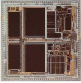
The SOC refers to integrating the different components of a system into a single IC. These components can be logic, memory or analog cores. Being a single die, an SOC is consequently fabricated using a single process technology. In addition, it has a single level of interconnections from the die to the package pads or to the interposer. The interconnection technologies used are wire bonding or flip chipping. Figure 1-1 presents an example of a SOC.
Figure 1-1: SOC example
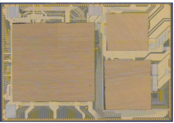
An attractive alternative for system integration is the SIP technology. The SIP concept started with the development of multi-chip module (MCM) in the 1990s. At that time, a typical MCM contained memories and a processor. Since then, the capacity of integrating several dies into a single package has continued to increase over time. Nowadays, a SIP may include analog and RF dies in addition to logic and memory ones, and even
fabricated with different process technologies, such as CMOS, BiCMOS, or GaAs. In addition, they are interconnected with multiple levels of interconnections: from die/component to die/component, or from die/component to the package pads or to the interposer. Several interconnection technologies can be used for this purpose, such as wire-bond, flip-chip, stacked-die technology, or any combination of the above.
An appropriate definition of a SIP is given in the International Technology Roadmap for Semiconductors published by Semiconductor Industry Association, where a SIP is defined as any combination of semiconductors, passives, and interconnects integrated
into a single package [SIA 2005]. This definition covers all the SIP technologies, which
differ in their type of carrier or interposer intended for holding the bare dies (or components) and the type of interconnections between components. The carrier or interposer can be a leadframe, an organic laminate, or silicon-based. Another possibility is to stack components on top of each other [Cauvet 2007]. Figure 1-2 shows an example of a silicon-based SIP fabricated by “NXP Semiconductors”, and characterized by:
- A passive die serving as platform for the active ones,
- High level integration of passive components in the passive die.
Figure 1-2: SIP example
I.1.B SOC versus SIP
The continuous advance in CMOS technology has led recently to a successful migration of RF and analog circuits from BiCMOS technology to a full CMOS solution. This important transition in the IC fabrication has permitted to a system with logic, mixed and analog functions to be designed as a single IC, namely as a SOC. As consequence, an interesting debate is launched: which is the better technology for a given system, to be designed as a SIP or as a SOC? Clearly, the better technology is dictated by the specifications and the constraints of the intended system. In the following we give a brief description of the main characteristics of both technologies, which are carefully considered by the system designers when they choose the SIP or SOC technology for their design.
With the SIP technology, the system can be designed in shorter time than a SOC. Each die can be separately designed in his most suited technology. Moreover, the SIP technology enables the plug-and-play approach. For example, considering an RF application system made of RF analogue mixed signal and digital dies, different RF designs can be done for different applications, without changing the baseband chip [Wilson 2005]. However, a system fabricated as a SIP is often more expensive than a SOC. fact, a SIP contains multiple pre-tested dies and passive components. They are
assembled together by a complex assembly process, where many different interconnect techniques may be used for wire bonding and flip-chip connections. In addition, the SIP technology uses some complex assembly processes that could reduce the system reliability, which is not the case of a SOC.
As result, the SIP technology seems to be more suitable for systems that have short production cycles, or for systems with short time-to-market. For example, in mobile phone applications, the system integrators came to the conclusion that integrating existing and available integrated circuits (ICs) into an SIP is often much easier and faster than creating new SOC designs [L-T. Wang 2008]. On the other hand, the SOC seems to be more suitable for high production volume, or for applications intended for a long run.
Anyway, both SIP and SOC manufacturers have to master the technology. This is one of the essential points to provide a reliable product, with the desired performances. However, this is not sufficient to provide a high quality product. In fact, due to the unavoidable flaws in the materials and masks used in the IC or SOC fabrication, a physical imperfection may be generated, leading to a defect in the fabricated IC or SOC. Similarly, during SIP fabrication several defects may be generated by the assembly process. Thus, any fabricated IC, SOC or SIP is considered to be defect prone. In consequence, all fabricated circuits and systems must be tested in order to filter the good from the defected ones. The following subsection presents an overview of the test principle and basics, focusing on digital IC testing.
I.2 Test principle and basics
In the microelectronic industry, a manufacturer is always interested to deliver a high quality product to its clients. For that, the fabricated circuits must be sufficiently tested before delivery. That is a must to maintain a good reputation, and to minimize the customer compliant as well. The good circuits are delivered, while the faulty ones can possibly undergo a failure mode analysis (FMA), which is typically used to improve the production yield, by giving a feedback to the product engineers in charge of the processes and products monitoring and improvement. The yield of a manufacturing process is defined as the percentage of acceptable parts among all manufactured parts:
fabricated parts of number Total parts acceptable of Number yield=
In the following, we give an overview of digital IC testing, where we describe the processes of test data generation and the equipments for test application. Next, we present the main features that are added to the IC design in order to improve its testability, before ending this subsection by detailing the JTAG boundary scan technique.
I.2.A ICs Test principle
Testing typically consists of transmitting test stimuli to the inputs of the device under test (DUT), while analyzing the output responses, as illustrated in Figure 1-3. The DUT
term designates an IC, a SOC or a SIP undergoing a test. DUTs that produce the correct output responses for all input stimuli pass the test and are considered to be fault-free. Devices that fail to produce a correct response at any point during the test sequence are assumed to be faulty.
Figure 1-3: Basic test principle [L-T. Wang 2006]
In digital IC testing, the test stimuli consist of a set of input patterns applied to the DUT. Each input pattern is a combination of logic 1’s and 0’s, called a test vector. Thus, in order to test a circuit with n inputs and m outputs, a set of test vectors is applied to the DUT, and its responses are compared to the known good responses of a fault-free circuit. Two processes are required for this purpose: the test generation and the test application. The test generation is the process of producing test vectors for efficient testing, whereas the test application is the process of applying those test vectors to the DUT and analyzing the output responses.
I.2.A.a. Test generation
Three approaches can be used in test generation: exhaustive, structural and (peudo)-random approaches. The exhaustive approach consists in applying all possible input combinations to the inputs (2n input patterns for an n-input logic circuit). This approach detects 100% of static defects that may exist in a combinational circuit; and the generation process is very simple. However, this strategy is not efficient for sequential circuits that require an ordered set of test vectors for every defect, which are necessary to reach required internal states. Thus, the 2n input patterns are not sufficient for sequential circuit testing. In addition, the test application process is too time-consuming in case of large value of n.
A more practical method, called structural testing is usually used for test generation. Based on circuit structural information, this approach uses a set of fault models to generate specific test patterns dedicated to the detection of these faults.
A fault model is an engineering model describing the possible physical defects that can occur in the fabricated device at a higher level of abstraction. By using fault models, the test vectors can be automatically generated by dedicated softwares. Common types of fault models are:
1. single and multiple stuck-at faults affecting the state of signals on the logic circuit lines,
2. delay faults that cause excessive delay along a path,
3. Transistor faults (stuck-open, stuck-short) that results in memory or non-logic behavior on gate outputs, open and short affecting the circuit wires.
A description of a single stuck-at fault is detailed as an example (see Figure 1-4). In this model, only one line in the circuit is faulty at a time. The fault is permanent, and its effect is as if the faulty node is tied to either Vcc (stuck-at-1 or s-a-1), or Gnd (stuck-at-0
or s-a-0). This model supposes that the function of the gates in the circuit is unaffected by the fault, this leads to a reasonable number of faults equal to 2*k, where k is the number of signal lines in the gate-level netlist of the circuit.
Input Test Stimuli Input1 Inputn Output1 Outputn Output Response Analysis Pass/Fail Device Under Test (DUT)
Figure 1-4: (a) True table of the fault-free AND gate, (b) fault model: s-a-1 on input A, (c) True table of the faulty AND gate
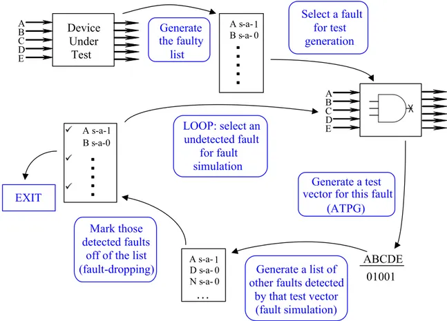
Using a fault model, the test generation begins by generating the faulty list, which contains all the potential faults. Then, a fault is selected for test generation, where an
automatic test pattern generator (ATPG) is used to generate a test vector for this selected
fault. Once generated, a fault simulation is performed to determine all faults that are detected by this test vector. Those detected faults are marked off of the list (fault-dropping). Then, another fault is selected from the remaining undetected faults in the faulty list, and the previous test generation steps are performed for this fault. This process is repeated until all the faults in the list are marked off, or the ATPG is unable to provide a test vector for the remaining faults. This is illustrated in Figure 1-5.
Figure 1-5: test generation process
Structural testing provides high quality test sequences, particularly for combinational circuits, but may require large CPU time. The process can be shortened using the (pseudo)-random approach as preliminary step. Random test vectors are first generated in order to remove the “easy to detect” faults from the faulty list. Easy-to-detect faults are those that can be detected by a large number of test vectors. In consequence, a vector generated randomly is likely to detect some of these easy-to-detect faults. A new pseudo-random test vector is generated until several successive generations fail to provide a test
Device Under Test A B C D E A s-a-1 B s-a- 0 Generate the faulty list Select a fault for test generation D B A E C Generate a test vector for this fault
(ATPG)
ABCDE 01001 Generate a list of
other faults detected by that test vector (fault simulation) A s-a- 1 D s-a- 0 N s-a- 0
…
Mark those detected faultsoff of the list
A s-a-1 B s-a-0 LOOP: select an undetected fault for fault simulation EXIT (fault-dropping) A B C 0 0 0 0 1 1 1 0 0 1 1 1 Vc c A B C (c) (b) A B C 0 0 0 0 1 0 1 0 0 1 1 1 (a)
vector detecting new fault in the list. At this point, the process switches to the deterministic and structural approach in order to generate test vectors for the remaining “hard-to-detect” faults.
Not that test vectors are generated for detection of faults and not defects. In other words, a test sequence including all the necessary vectors for detection of faults in a model, stuck-at faults for instance, cannot guarantee the detection of all possible manufacturing defects.
I.2.A.b. Test application
As already mentioned, the test application designates the process of applying test vectors to the DUT and analyzing output responses. This process is performed by
automatic test equipment (ATE), which contains typically the following main
components:
1) A powerful computer: it represents the interface between the user and the tester, stores the test program, including test data and responses, timing and level information.
2) A main frame and/or a test head: it include(s) all the electronics that are necessary to perform the test (level and timing generators, power supply, vector memory, all necessary pin electronic for driving and reading values on the tester channels). Under the control of the test program, the tester electronics translate test patterns into corresponding electrical waveforms with the desired shape and timing, compare (or measure) DUT output responses to expected values, and return pass/fail information to the computer.
3) DUT board and probe card: they are used as an interface between the electronics of the tester and the DUT IOs. Their goal is to provide electrical paths for power supply and test signals transfer between the tester electronics and the pads of an IC on a wafer or the pins of a packaged chip during testing. The contact elements of the probe card are called probe tips.
The ATE may contain other resources such as digital signal processors (DSP), used for analog testing. Regarding the various components of an ATE, this later can be very expensive. The pin electronics and the correspondent probe card are typically the most expensive part of the ATE.
To summarize, the digital IC testing consists in generating logic values of the test vectors (ATPG program), based on fault models. An ATE is used to apply those test vectors to the DUT and to analyze the output responses. Depending on the complexity of the DUT, the test generation process may take a long time to generate a set of test vectors detecting all faults; in some cases, some faults remain undetectable, which reduces the test quality.
In order to decrease test generation and test application times and to enhance test quality, testability-related design rules are used during the circuit design. This will be explained in the following subsection.
I.2.B Design for testability
Integration of design and test consists in considering testing early in the design flow. This task is referred as design for testability (DFT). Related techniques are usually
classified into three categories: Ad-hoc DFT techniques, Scan design, and built-in
self-test (BIST).
I.2.B.a. Ad-hoc DFT techniques and Scan design
The goal of such techniques is to enhance the capabilities of controlling and observing the poorly testable nodes in a circuit. Doing so, the test generation is easier, the quality of test is improved, and the test, debug and diagnose tasks are simplified.
Ad-hoc methods target the difficult-to-test protions of the circuit and consist in adding dedicated circuitry (test points) for controllability and observability improvement. The test points allow to access circuit internal nodes directly.
Scan design is the most common DFT technique used for sequential circuits. All or a part of the storage elements (latches or flip-flops) in the IC design are made externally controllable and observable. An extra circuit signal called scan enable is added to the design. When asserted, the storage elements, called scan cells, are stitched together to form one or several shift register(s), called scan chain(s). Each scan chain is connected to one primary input and one primary output. Thus, an arbitrary pattern can be serially entered into the chain of flips flops, and the state of every flip flop can be read out. Therefore, the problem of sequential testing becomes one of combinational logic testing only, leading to an easier test generation process, and better test quality. An example of full scan design circuit is shown in Figure 1-6.
Figure 1-6: sequential circuit (a) designed as full scan circuit (b).
Another important technique based on test data serialization is the JTAG boundary scan test introduced for board testing. Since our work, presented in chapters 2 and 3 of this document, is heavily based on this technique, this later will be described in details in section I.2.C.
I.2.B.b. BIST techniques
The BIST is a design technique consisting in integrating in the DUT a test pattern
generator (TPG) and an output response analyzer (ORA) in order to perform testing
internal inside the IC. The TPG generates the test vectors applied to the DUT inputs, while the ORA automatically compacts the output responses of the DUT into a signature. The operations of the TPG, the DUT and the ORA are controlled by a logic BIST controller. This later provides all the necessary timing control signals to ensure a correct testing operation. Once the BIST operation is complete, the BIST controller provides a pass/fail indication after comparison of the final signature with a golden signature. Figure 1-7 shows an example of DUT with logic BIST structures.
Figure 1-7: typical logic BIST structure
Clearly, the BIST technique generates an important area overhead, since it implies the integration of the TPG, ORA and logic controller in the DUT. However, BIST techniques offer many advantages that can favorite their use:
- In fact, the test time is reduced with BIST. In consequence, the test cost is reduced on its turn, which alleviates the cost of the area overhead.
- BIST techniques permit to avoid the use of high expensive ATE, as most of the tester functions reside on-chip itself.
- BIST techniques offer the possibility to perform a reliable test of internal circuit components, in case of limited external access via the primary inputs.
- BIST can be used from wafer to in-situ testing. I.2.C JTAG boundary scan
The joint test action group (JTAG) TAG was an industry group formed in 1985, which has developed a specification for boundary-scan testing that was standardized in 1990 [IEEE 1149.1 Std]. In 1994, a supplement containing a description of the boundary-scan
description language (BSDL) was added to the standard. Since that time, JTAG has been
adopted by major electronics companies all over the world. Applications are found in high volume, high-end consumer products, telecommunication products, defense systems, computers, peripherals, and avionics.
The boundary-scan test architecture provides a means to test interconnects between integrated circuits on a board without using physical test probes. Its basic idea consists in adding scan registers to the inputs and outputs of ICs, as shown in Figure 1-8.
Figure 1-8: basic idea of boundary scan
The boundary scan cells of ICs on the same board are interconnected into a single boundary-scan chain (see Figure 1-9). Through this chain, the I/Os of each IC are
Boundary scan registers
controllable and observable via serial scan and Capture/Update operations. Thus, a pattern can be applied to the circuit inputs, and the response can be read out via the boundary scan chain. This can be used to test the soldered ICs on a board, as well as the interconnections between them.
Figure 1-9: a board containing four ICs complying with boundary scan
I.2.C.a. Test architecture and procedure
In addition to the boundary-scan register, extra control circuitry is implemented. The boundary-scan circuitry can be divided into four main hardware components:
• A Test Access Port (TAP), which represents the circuit test interface.
• A TAP controller (TAPC), which is a 16-states finite-state machine that controls each step of the boundary-scan operations.
• An instruction register (IR), and its associated decoder.
• Several test data registers, including mandatory register like a Bypass register, and some optional registers like device-ID register.
Figure 1-10 shows the architecture of a boundary scan compliant circuit. Each of the four main components is detailed in the following sub-sections.
Figure 1-10: Compliant digital die with IEEE 1149.1
Internal logic Serial data in Serial data out Boundary-scan cell
Boundary-scan chain System interconnections
Internal logic Internal logic Internal logic Boundary Scan cell Boundary Scan Path Instruction Identification Bypass Bypass Die Core Sout Sin TDO TDI IN1 OUT1 OUT2 OUT3 OUT4 IN2 IN3 IN4 TCK TMS interne Scan T A P C o n tr o ll e r TRST
In addition to extra hardware components, the IEEE 1149.1 std. also defines a set of test instructions, including four mandatory ones (BYPASS, SAMPLE, PRELOAD, and EXTEST), and several optional ones.
An outline of test procedure using boundary scan is as follows:
1. A boundary-scan test instruction is shifted into the IR through the TDI.
2. The instruction is decoded by the decoder associated with the IR to generate the required control signals so as to properly configure the test logic.
3. A test pattern is shifted into the selected data register through the TDI and then applied to the logic to be tested.
4. The test response is captured into some data register.
5. The captured response is shifted out through the TDO for observation and, at the same time, a new test pattern can be scanned in through the TDI.
6. Steps 3 to 5 are repeated until all test patterns are shifted in and applied, and all test responses are shifted out.
I.2.C.b. Test access port
The TAP of 1149.1 contains four mandatory pins and one optional pin, as described below:
• Test Clock Input (TCK): is a clock input to synchronize the test operations
between the various parts of a chip or between different chips on a PCB. This input must be independent of system clocks, so the shifting and capturing of test data can be executed concurrently with normal system operation.
• Test Data Input (TDI) is an input to allow test instructions and test data to be
serially loaded respectively into the instruction register and the various test data registers.
• Test Data Output (TDO) is an output to allow carious test data to be driven out.
Changes in the state of the signal driven through TDO should occur only on the falling edge of TCK.
• Test Mode Select (TMS) is the sole test control input to the TAP controller. All
boundary-scan test operations such as shifting, capturing, and updating of test data are controlled by the test sequence applied to this input.
• Test Reset (TRST) is an optional pin used to reset the TAP controller.
I.2.C.c. Data registers and boundary-scan cells
Standard 1149.1 specifies several test data registers, as shown in Figure 1-10. Two mandatory test data registers: the boundary scan register and the bypass register, must be included in any boundary scan architecture.
a) Boundary-scan registers (BSR)
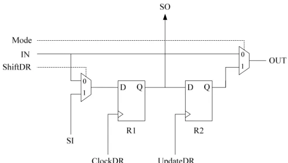
BSR is the collection of the boundary- scan-cells (BSCs) inserted at the I/O pins of the original circuit, as shown in Figure 1-10. A typical BSC is shown inFigure 1-11.
Figure 1-11: a typical boundary scan cell
This cell can be used as either an input or output cell. As an input cell, the IN signal line corresponds to a chip input pad, and the OUT signal line is tied to an input of the internal logic. As an output cell, IN corresponds to the output of the internal logic, and OUT is tied to an output pad.
The test operations of a BSC are controlled by three output signals of the TAP controller: ClockDR, ShiftDR, and UpdateDR. There are four major modes for the boundary-scan cell:
- Normal mode: simply passes inputs to outputs. (Mode = ‘0’).
- Scan mode or shift mode passes data from SI to R1 and from R1 to SO. (ShiftDR =
‘1’, ClockDR = clock pulse).
- Capture mode loads the value on the input IN to R1. (ShiftDR = ‘0’, ClockDR =
clock pulse).
- Finally, update mode loads values from R1 to the output. (Mode = ‘1’, UpdateDR
= 1 clock pulse).
To shift in data, the scan mode must be selected for a number of clock cycles. This number is dictated by the number of scan cells in the scan chain. Once the shift operation is complete, the update mode is selected for only one clock cycle to apply the data. To capture data and scan it out, one cycle of capture mode must be selected followed by the required number of scan cycles.
b) Bypass register
Bypass register is a single-bit register that is used to bypass a chip when it is not involved in the current test operation. This can significantly reduce test time required to shift in/out test data through the long TDI-TDO system path.
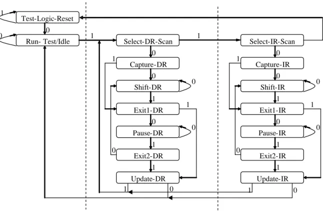
I.2.C.d. TAP Controller (TAPC)
The TAPC is a 16-states finite state machine, which operates according to this state diagram.
Figure 1-12: state diagram of TAP Controller
According to the state diagram shown in Figure 1-12, we give the data scan timing diagram as an example of test logic operation, shown in Figure 1-13.
R u n -T es t I d le S el ec t-D R -S ca n C ap tu re -D R S h ift -D R E x it1 -D R P au se -D R T es t-L o g ic -R es et Instruction IDCODE
Old Data New Data
Output inactive
Output from selected data register TCK TMS Controller state TDI Data input IR shift register Parallel output of IR Data input to DR TDR shift register Parallel output of TDR TDO Don’t care E x it2 -D R S h ift -D R E x it1 -D R U p d at e-D R R u n -T es t I d le S el ec t-D R -S ca n S el ec t-IR -S ca n R u n -T es t I d le S el ec t-D R -S ca n C ap tu re -D R S h ift -D R E x it1 -D R P au se -D R T es t-L o g ic -R es et Instruction IDCODE
Old Data New Data
Output inactive
Output from selected data register TCK TMS Controller state TDI Data input IR shift register Parallel output of IR Data input to DR TDR shift register Parallel output of TDR TDO Don’t care E x it2 -D R S h ift -D R E x it1 -D R U p d at e-D R R u n -T es t I d le S el ec t-D R -S ca n S el ec t-IR -S ca n
Figure 1-13: timing diagrams in scan operation [IEEE 1149.1 Std]
Test-Logic-Reset
Run- Test/Idle Select-DR-Scan
Capture-DR Shift-DR Exit1-DR Pause-DR Exit2-DR Update-DR 0 0 0 0 0 0 0 0 0 1 1 1 1 1 1 1 1 1
Select-IR-Scan
Capture-IR Shift-IR Exit1-IR Pause-IR Exit2-IR Update-IR 0 0 0 0 0 0 0 1 1 1 1 1 1
I.2.C.e. Instruction register and instruction set
The instruction register (IR) is used to store the instruction to be executed. The decoder associated with the IR decodes the instruction to generate the required control signals. Four mandatory boundary-scan test instructions (SAMPLE, PRELOAD, BYPASS, and EXTEST) are defined in 1149.1. In addition, the INTEST instruction is recommended. There are other useful instructions such as USRCODE, IDCODE, CLAMP… but they are not described here.
BYPASS: this instruction is used to “bypass” the boundary-scan registers on unused chips so as to prevent long shift operations.
SAMPLE: the sample operation can be completed when the Capture operation is executing, such that the required test data can be loaded in parallel to the selected data registers. This means that a snapshot of the normal operation of the chip can be taken and examined.
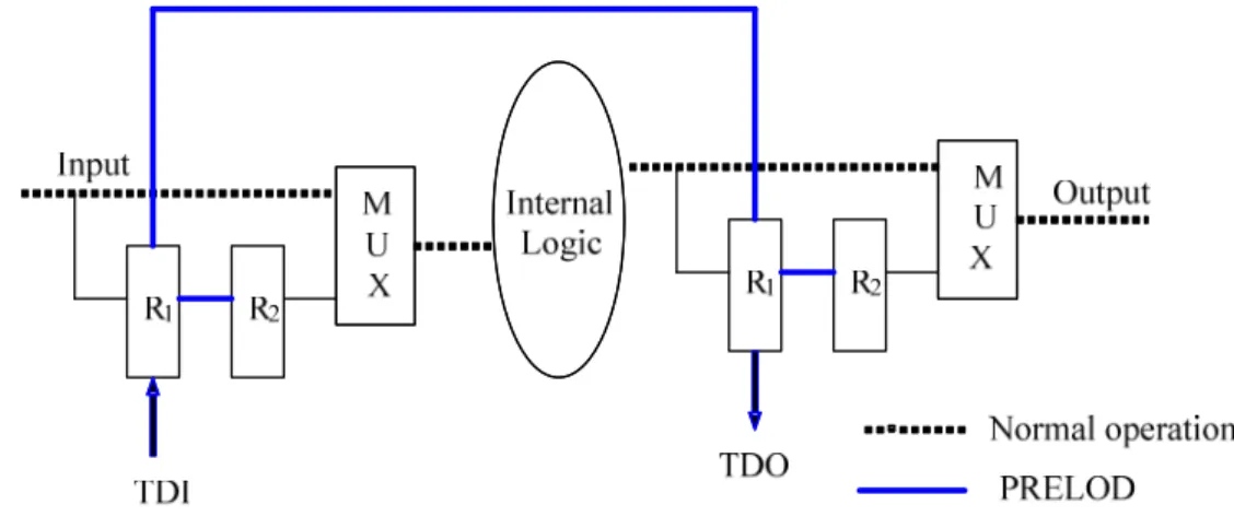
PRELOAD: this instruction allows test data to be shifted into or out of the selected data register during the Shift-DR operation, without causing interference to the normal operation of the internal logic (see Figure 1-14). This allows an initial data pattern to be placed at the latched parallel outputs of boundary-scan test operation.
Figure 1-14: execution of PRELOAD instruction
EXTEST: this instruction is used to test the circuitry external to the chips, typically the interconnections between chips and between boards.
There are other versions for the standard IEEE 1149, such as 1149.4 [IEEE 1149.4] which is created to standardize the boundary scan for analog test, and 1149.6 [IEEE 1149.6], which is intended for advanced digital networks that include analog components and high speed I/O ports.
I.3 Testing at various manufacturing stages: test application issues
The microelectronic circuits go through several fabrication steps, prior to their exploitation by the end user. Taking account of the possible defaults which could be generated by the fabrication process, the circuits are tested at the end of each fabrication step. Only the fault-free circuits move to the next step, where the defected circuits are discarded in general.
The lifecycle of a circuit begins when the designers provide the circuit design masks. These latter are used to fabricate the circuits on a silicon wafer. Once the fabrication is complete, the circuits first undergo the “wafer test” (Figure 1-15), where the faulty ones
are marked to be discarded after wafer dicing. The next manufacturing step is packaging (for simple IC or SOC) or assembly with other circuits (in case of bare dies to be included in an SIP before packaging of the complete system. Once packaged, the chips undergo another test before delivery, named “final test”. The packaged circuits or systems that pass the final test are delivered to the board or product manufacturer. Delivered IC and systems are then assembled onto a printed circuit board (PCB). The PCB is tested before and after assembly of the components in order to check the interconnections and the assembly process. Later, this PCB is integrated in the final product, which is tested before sale. At this point, the fabrication flow of the IC is finished, where it is now ready to be exploited by the end user.
Some applications require test and diagnosis during the chip lifetime, which means to perform an in-situ test.
Figure 1-15: IC manufacturing and test steps
A short state-of-the-art of the wafer test technologies is presented in section I.3.A to exhibit the major technological problems. Once the circuits are packaged, the compound needs to be tested again: in section I.3.B, we will see what the most critical issues are. Some considerations will be additionally addressed in sections I.3.C and I.3.D, dealing with the board and the in-situ test issues.
I.3.A Wafer testing issues
Manufacturers try to catch the defects at the earliest stages of the circuit life for both cost savings and quality improvement. Indeed, every late detected defect represents a significant loss, and it is even more costly if it is detected by the customer after delivery. The preferred strategy therefore consists in reaching the highest possible coverage during the wafer test, to minimize the yield losses at final test. A test applied to a bare die is usually called ‘wafer test’ while a test applied to a packaged IC is called ‘final test’.
Clearly, an ATE must be connected to the primary I/Os of the DUT when test is applied. During wafer test, this connection is done with the IC pads through a dedicated
probe card. The physical contact between the DUT pads and the probe tips is called a
touchdown.
This contact-based technology suffers from several limitations and problems. For example, after testing a number of DUTs on a wafer, debris can accumulate on the tips of the probe needles due to repetitive touchdowns. This can affect the probe card efficiency and reduce the test quality in consequence. Thus, the probe tips must be periodically
cleaned. In the following, we address the major technological problems of current probing techniques. Next subsection presents different probing technologies and general related issues. The following section is dedicated to issues related to SIP testing.
I.3.A.a. Probing technologies and limitations
Probe cards are classified according to their probe tips type. The traditional technology is based on tungsten needles shaped in a cantilever profile. The shaft of each needle is held in place by an epoxy ring (seeFigure 1-16.) This technology remains one of the most widely used technologies in the probe card market today [Mann 2004].
Figure 1-16: Principle of cantilever probe card [L-T. Wang 2008]
This technology suffers from pads scratching. In addition, the number of DUTs that can be concurrently tested (parallel test) with cantilevers probe card is very limited. In fact, two limiting factors are caused by the volume and the shape of the cantilevers: the alignment of probe tips and the important space required by the probe needles -dedicated to one DUT- above the wafer. Typically, the number of DUT concurrently tested with this type of probe card is limited to two.
The vertical probe is an alternative probing technology appeared in 1977. Basically, this technology was developed to fulfill the requirements for array configurations. An array configuration designates an IC design where the I/O pads are placed over the entire IC surface rather than being restricted to the perimeter. Recently, with the increasing demand for concurrent test, the vertical probe technology has known a growing use. Its principle is depicted in Figure 1-17.
Figure 1-17: principle of vertical probe card [Mann 2004]
The “membrane” technology is a particular type of vertical probe cards, basically developed for RF IC testing. By reducing the distance between the pads and the test head
components, the membrane technology permits a better transfer of analogue and RF signals from the ATE to the DUT. Thus, the problems of signal attenuation and noise interference, encountered with classical probing techniques, are resolved. The membrane technology is illustrated in Figure 1-18. The signals transfer from the ATE electronics to the DUT is done through a set of micro-strip transmission lines, which are designed on a flexible dielectric material. The DUT is contacted by an array of micro-tips formed at the end of the transmission lines through “via holes” in the membrane (Figure 1-18.a) [Leslie 1989], [Leung 1995], [Wartenberg 2006]. The membrane is mounted on a PCB carrier that interfaces with the test board (Figure 1-18.b).
(a) Membrane technology
(b) Structure of the probe card
Figure 1-18: Membrane probe card [Leslie 1989]
In general, the vertical probe technology permits to test several DUTs in parallel, as much as the tester resources can support. However, this concurrent test is limited by the co-planarity factor. In fact, when test is applied, all vertical probes must contact the dedicated pads on the DUTs. A pressured touchdown may cause damaging to the DUTs, whereas a relaxed touchdown may leave some pads without contact. Therefore, it is preferred to test a limited number of DUTs with correct probing, rather than testing a higher number of DUTs with risked probing.
The vertical probe implies that the pad size and pitch (minimum distance between two pads) must be large enough to perform a correct contact with the vertical probe needles. However, pad size and pitch have regularly decreased, requiring more and smaller probe needles, and forcing probe cards therefore towards novel technologies. In addition, the growth of chip-scale and wafer-level packages put further demands on probes, which must contact now solder bumps instead of planar pads [L-T. Wang 2008].
Contact bumps Membrane Microstrip transmission line Ground plane Contact bumps Membrane Microstrip transmission line Ground plane Carrier PCB Membrane Forced-delivery mechanism Contact bumps Terminations and bypasses Carrier PCB Membrane Forced-delivery mechanism Contact bumps Terminations and bypasses
An emerging technology, based on MEMS implementation of probe needles, is recently developed to push the mechanical limits forward. With this technology, the volume of probe needles is significantly reduced. Thus, pitches of 35µm can be achieved with minimal scratching risk, and a higher number of DUT can be tested in parallel. MEMS based probe cards are now starting to replace the traditional ones, where industrial products and research demonstrations show a growing interest in the MEMS-based technologies [Cooke 2005]. However, this novel technology -currently under development- is very expensive. In addition, like other technologies, it suffers from the debris problem. In fact, due to the probe needle reduced size, debris can rapidly accumulate on the MEMS cantilevers. Moreover, it needs more time to become sufficiently reliable. For that, this technology is not used today for high production testing.
Table 1-1 summarizes the main advantages and problems of probing technologies.
Advantages Drawbacks
Cantilever simple and cheap - pads scratching - limited parallel test - debris problem Vertical - large parallel test
- testing of array configuration - reliable RF test (membrane technology)
- size and pitch of pads are limited - planarity problem
- debris problem
MEMS - bond pads probing - enhanced parallel test - reduced pitch size
- no serious scratching problem
- very expensive
- not a mature technology (still under development)
- debris problem
Table 1-1: advantages and drawbacks of various probing technologies
To summarize, various probing technologies have been developed for IC testing. Each technology presents some advantages but suffers from several limitations at the same time. The reduction of the size and the pitch of the pads, the development of very complex devices, beside the increasing demand for multi-site (parallel) testing, have pushed the fabrication of probe cards towards the limits of the technology. However, even with the most advanced probing techniques, the wafer test stills suffer from contact problems, and it is expected to not be able to catch-up with the increasing requirements for high speed and high frequencies test needed for the complex circuits [Wu 2006].
In this section, we have discussed the major technological problems concerning the wafer test for any type of circuit. Additional limitations that are related to SIP testing are discussed in the next section.
I.3.A.b. SIP testing and related issues
A SIP is a sophisticated system, including multiple pre-tested dies and passive components. They are assembled together by a complex assembly process, where many
different interconnect techniques may be used for wire bonding and flip-chip connections. Thus, the resulting SIP is an expensive product. Knowing that a defective SIP cannot be repaired, we come therefore to the following observation [L-T. Wang 2008]:
“The SIP process is economically viable only if the associated yield YSIP of the
packaged SIP is high enough”.
Considering an SIP assembly process including n different dies, the overall yield YSIP
can be ascertained by the Equation 1-1 [L-T; Wang 2008]:
YSIP = 100 [P1 × P2× … × Pn] × Ps × PintQ × Pw . (1-1)
Where Pi is the probability that die #i is defect-free, Ps is the probability of
manufacturing a defect-free substrate (possibly including passive components), Pint is the
probability of die interconnect being defect-free, Q is the quantity of die interconnects, and Pw is the probability of placement and mounting being defect-free.
The previous equation shows that the overall yield of a SIP manufacturing process depends on the quality of assembled components, as well as on the quality of the assembly process. In fact, complex process may create new failures, because:
- More stress is applied during assembly, which may cause die cracks, or broken bonding.
- Placement of active dies on passive die is a potential source of misalignment, i.e. shift and rotation (see Figure 1-19)
Figure 1-19: possible misplacement during assembly process:shift (left), and rotation (right).
Thus, dies must be of a high quality and the assembly process must be under control in order to achieve a viable yield. For that, a special strategy can be followed during SIP manufacturing process. It consists of:
1. Use of known good dies (KGD) in SIP fabrication. A KGD is a bare die with the same, or better, quality after wafer test than its packaged and “final tested” equivalent [Cauvet 2007].
2. An assembly process beginning by the cheaper die and finishing with the most expansive one, and
3. A recursive test after the assembly of each die, in order to avoid the loss of expensive dies not yet assembled, if any default is detected at current assembly phase.
However, recursive test requires several touchdowns on SIP pads. Even with the advanced probing techniques, performing several touchdowns may lead to substrate pad scrubbing (see), which may affect the quality of wire bonding.
Figure 1-20: pad scrubbing due to several touchdowns (source :NXP semiconductors)
For this reason, the number of touchdowns is typically limited to three. In consequence, the number of assembled active dies is limited to two, since a preliminary test of the substrate is usually performed before to start the assembly process. Regarding the previous limitations of contact-based probing techniques, alternative solutions must be investigated for the particular case of SIP testing during manufacturing.
I.3.B Final testing
After wafer dicing, the expected fault-free devices (IC, SOC or SIP) are packaged. A package consists typically of a “lead frame” intended to hold up the bare device, and a kind of box intended to cover this device. The packaging process consists in putting the bare device on the lead frame, interconnecting the die pads to the lead frame pins, and finally fixing the box on the leadframe, creating therefore the final package. Once packaged, the circuits are tested before their delivery. This test is called final test.
In general, the final test tries to detect the possible defects caused by wafer dicing or packaging process, as well as to cover the misses of wafer test. Even when manufacturers try to guarantee the quality of the bare dies by an efficient wafer test, this objective is not easy to reach because of many limitation factors, such as limited contact and probe speed. Fortunately, these limitations do not exist in final test, where the contact is performed with the package pins instead of circuit pads. Moreover, high speed and high frequencies can be handled more easily than at wafer level [Mann 2004].
The final test consists in a combination of functional and parametric test. The functional test consists in applying a set of test vectors at the input of the DUT and verifying if the output responses are equal to the expected ones. The parametric test consists in verifying the limit values of circuit parameters. Two types of parametric test:
1- DC parametric test: it consists in measuring a DC current or a DC voltage
during test application. According to the measured value, a “pass/fail” decision is done at the end of test.
2- AC parametric test: it permits to measure the dynamic parameters of a
circuit: width of the clock pulse, propagation time, set-up time, hold time, fall time, etc…
After final test, the packaged circuits are delivered to the customer. Each delivery is characterized by a defect level (DL). A DL, called reject rate also, is the ratio of delivered faulty parts to the total number of delivered parts:
parts delivered of number Total parts faulty delivered of Number rate Reject =
A reject rate of 300 parts per million (PPM) chips or less may be considered to be
acceptable for mobile phones, while 100 PPM or lower represents good quality for home consumer devices. A reject rate of 10 PPM or less is needed for automotive applications. I.3.C Board and product testing
Traditionally, the circuits on board have long been tested using a “Bed of Nails”, usually combined with functional testing of every chip. However, this approach has several drawbacks. In fact, a Bed of Nails, basically used to create test access, requires the addition of “test-lands” to the PCB, which generates a significant board area overhead. In addition, fast functional tests are used to test the chips. These tests can target chip damages due to the assembly process but do not provide high fault coverage like a structural test for instance. To overcome these drawbacks, the current test strategy consists in using only “fault-free” chips and the JTAG boundary scan standard [van Geest 2001], [Schuttert 2004]. Following this strategy, the assembled circuits are considered fault-free components (high quality testing must thus be performed on every component before system assembly). Consequently, the board testing can be limited on faults possibly introduced during the PCB assembly process. That leads to focus the test on the interconnections between the circuits, in addition to a partial test of the circuits themselves to ensure that they are not damaged during the assembly process.
Following this strategy, the JTAG boundary scan technique is strongly adopted for interconnections test. Thanks to the analogue extension of the boundary scan standard (IEEE 1149.4), digital and analogue interconnections can be easily tested at board level. Concerning the test of the chips soldered on the board, the JTAG boundary scan infrastructure allows accessing extra test resources introduced by the DFT activity on every chip.
Figure 1-21: novel strategy of PCB assembly test [van Geest 2001]
components assemblies applications
(ICs) (PCBs) (SW)
test
DfT
DfT
DfT
DfT
growing
silicon
content
more
features
squeeze
PCB assembly
costs & time
To summarize, a novel strategy for board testing has been suggested. It consists in building or re-using on-chip test solutions (DFT), beside JTAG boundary scan for convenient test access. With this trend, the area overhead, costs and development time of board testing can be significantly reduced (see Figure 1-21).
As for components at lower level of integration, parallel and concurrent testing of several boards leads to save test application time. However, physical and contact-based accesses to several boards at a time require the development of a dedicated test infrastructure, where the test data could be broadcasted to a large number of boards. I.3.D In-situ test
As discussed earlier, testing an integrated circuit or system at manufacturing time is a must to guarantee a high quality product, and After delivery, the device undergoes another test when it is assembled to the dedicated system (e.g. PCB). This last test aims to detect the possible defaults generated by the assembly process.
Once the system is successfully assembled, it becomes ready for use, and therefore, to begin its application lifetime. However, some applications need to test and diagnosis the devices on board or system during their active lifetime, which is the case for critical application (e.g. automotive, medical implants …). However, in order to perform an in-situ test, we need to satisfy two conditions:
- First, we need to provide an external access to the device embedded within the
system.
- Secondly, this access must be reliable and non-intrusive as well.
In several cases, a wired contact with the DUT is not possible. This can be the case of circuits embedded in a satellite or a vehicle for example, or the case of medical implants in a human body. Thus, an attractive solution for such cases consists in using the wireless communications, where it provides a non-intrusive access to the DUT for in-situ test purpose.
I.4 Conclusion
Because defects created during the chip manufacturing process are unavoidable, the test activity plays a key role in this process by its ability to differentiate good devices from faulty ones before delivery to end-users, and to improve the manufacturing yield, where it permits to analyze and correct the causes of defects when encountered. Basically, testing consists of two processes: the test generation and the test application. Test generation designates the process of providing test vectors, whereas the test application refers to the process of applying those generated vectors to the DUT inputs and analyzing the responses.
As the microelectronic devices continue to shrink in size and increase in density, testing these devices has become increasingly difficult. In fact, while the number of primary I/O is stable, the integration of different cores in the same chip (SOC) or in the same package (SIP) continues to grow up. In consequence, the number of tests that must be applied to a manufactured circuit has increased, while the test access from primary inputs remains relatively limited. Thus, test generation becomes more complicated, implying a higher cost and a longer development time. To solve the previous issues, DFT techniques are increasingly adopted for circuits testing. The test application consists in applying the test stimuli from an ATE to the DUT and in collecting test responses from the DUT through a dedicated interface. As previously mentioned, the test application
suffers from several drawbacks and limitations according to the DUT (IC, SOC, or SIP) and the considered manufacturing or integration step.
At wafer test time, the ATE is connected to the DUT pads through a probe card. Various technologies of probe card have been elaborated for IC wafer testing, but every one has its limitations. The traditional probing technology, based on tungsten needles shaped in a cantilever profile presents a limited parallelism (number of dies on a given wafer that can be tested at a time) [L-T. Wang 2008]. In addition, it suffers from pad scratching and debris problems. These later ones are common also to the vertical probing technology [Mann 2004]. Moreover, it is expected that the vertical technology will not be able to catch up with the continuous decrease of pad size and pitch. Recent probing technology based on MEMS cantilever is currently under development, pushing the mechanical limits forward. However, this technology is very expensive and suffers also from debris problem.
Parallel testing of numerous devices (from bare dies to boards) is always a challenge due to the difficulty to contact numerous devices at a time. Additionally, in-situ testing encounters the problem of missing a reliable external access to IOs of the DUT embedded in the system. Finally, the particular case of SIP testing, which requires several touchdowns during the assembly process, increases the problems related to test application based on physical contacts between probe cards and DUT.
In result of all these contact-based test technology related issues (test costs, limited parallelism, pad scrubbing, in-situ testing) a test technology based on wireless transmissions appears as a possible alternative. For that, we propose a new wireless test solution, which can be used at various levels of manufacturing process. Before describing this solution, we give an overview of the wireless test methods currently under development in the next section.
II
State of the art of wireless test methods
Several wireless or contactless test methods were recently proposed to solve the probing-related or contact-related issues. In this section, we first address the main challenges related to test strategies based on wireless communication, and we give a detailed description of several related methods proposed so-far for wafer or in-situ test. In the following, “wireless test” stands for test application strategies using wireless or contactless communications for transmission of test data between the test equipment and the DUT.
II.1 Wireless test challenges
The wireless test is proposed to solve the problems of contact-based test. Its purpose consists in transferring the test signals from the ATE to the DUT through a wireless link, to get rid of the probe needles and their limitations. Clearly, a wireless test interface must be added to the ATE and to the DUTs for this purpose. In consequence, some modifications must be done at design time in order to provide a wireless interface to the DUT, and classical test procedure must be adapted as well. These modifications generate new critical issues that must be addressed in any proposed wireless test approach, mainly the following ones:
- Power supply: In classical probing techniques, the ATE delivers the power and clock signals to the DUTs through the probe needles. However, no contact is
envisaged with the DUT in wireless test; and therefore, an alternative solution must be provided to deliver power and clock signals.
- Area overhead: clearly, an antenna and a RF transceiver and possible extra logic must be integrated in the DUT. The resulting area overhead is a critical issue that must be carefully considered.
- Transmission reliability: the reliability of the wireless communication is crucial. The bit error rate (BER) of the transmission must be very low. The possible errors of the RF transmission must not generate any error in the test application.
- MAC protocol: in order to establish a good communication between the ATE and the DUT(s), an efficient medium access protocol (MAC) must be used.
- Transparent solution: it is highly preferable that a proposed wireless solution do not imply any modification on the test generation process. Thus, the test programs and software remain unchangeable with wireless test.
- Test data management: once generated, the test data are transported from the tester to the DUT in wireless manner. Generally, the data are transmitted in packets. Thus, the DUT must be able to extract the test data from the received packets, and generates a packet to transmit its response, as well.
- Types of test: an interesting method is who permits to perform the large types of test, such as JTAG boundary scan, or BIST application that is not accessible through JTAG interface, etc…
- Security: the access to the internal circuit structures through the embedded wireless interface must be denied for anyone, except the person in charge of performing the test.
- Multi-usage: a powerful method is that which can be used at several stages of manufacturing (e.g. wafer test and in-situ test).
II.2 Scanimetrics approach
An emerging solution for wafer test was recently developed by “Scanimetrics”, a Canadian company. It consists of replacing the traditional probe card by a non-contact interface [Moore 2008], [Moore 2007], [Sellathamby 2005]. Following this approach, each probe needle is replaced by a couple of antennas and transceivers. A first “antenna & transceiver” is connected to the DUT pad, and a second “antenna & transceiver” is integrated in the probe card. Thus, a probe card with n probe needles is replaced by a probe card with n micro antennas and transceivers. On the other side, the DUT integrates equally n micro antennas and transceivers connected to n pads, and operating at the same carrier frequency. The communication between the probe card and the DUT is performed pad to pad; where near field communication (NFC) is used to transfer data at tens of megabit per second rates. The distance between the probe card and the DUTs is up to 100 µm, depending on the antenna size. The principle is depicted in Figure 1-22 and Figure 1-23.
Figure 1-22
Figure 1-23: Cross
This novel technology offers many advantages including:
- High reliability of wireless communication due to the short - Since the communicati
is no need neither for MAC protocol, neither for data processing.
- Low complexity of the added DfT in the DUT (antennas and transceivers), - The additional area overhead is negligible
be implemented in a small area varying from 7200 µm 2006], [Sellathamby
which increase when the distance between the wireless probe card and the DUT increases. Note that, this overhead area is added to each pad, which must be multiplied by the number of wireless pads to calculate the global area overhead (e.g. 62500 µm2 x 5, in case of JTAG test because of 5 JTAG signals requiring 5 wireless pads)
- The proposed solution is completely transparent for the actual test software, - Various types of test such as scan chain,
solution, P ro b er T es te r P ro b er T es te r
22: Scanimetrics principle of non-contact testing (Courtesy of Scanimetrics)
Cross-sectional view of the non-contact test solution (Courtesy of Scanimetrics)
This novel technology offers many advantages including:
High reliability of wireless communication due to the short-range communication ince the communication is performed from pad to pad (without packets), so there is no need neither for MAC protocol, neither for data processing.
Low complexity of the added DfT in the DUT (antennas and transceivers), The additional area overhead is negligible. In fact the antenna and trans be implemented in a small area varying from 7200 µm2 to 62500 µm
Sellathamby 2005], according to antenna size and transceiver which increase when the distance between the wireless probe card and the
Note that, this overhead area is added to each pad, which must be multiplied by the number of wireless pads to calculate the global area overhead x 5, in case of JTAG test because of 5 JTAG signals requiring 5 olution is completely transparent for the actual test software,
Various types of test such as scan chain, JTAG, etc… can be performed with this Signal Distribution Signal Transfer Intelligent Test Circuits Parametric Test Circuits Tx/Rx Tx/Rx Tx/Rx Tx/Rx Tx/Rx Power Tx/Rx Tx/Rx Tx/Rx Tx/Rx Tx/Rx
Probe Card Device Under Test Signal Distribution Signal Transfer Intelligent Test Circuits Parametric Test Circuits Tx/Rx Tx/Rx Tx/Rx Tx/Rx Tx/Rx Power Signal Distribution Signal Transfer Intelligent Test Circuits Parametric Test Circuits Tx/Rx Tx/Rx Tx/Rx Tx/Rx Tx/Rx Tx/Rx Tx/Rx Tx/Rx Tx/Rx Tx/Rx Power Tx/Rx Tx/Rx Tx/Rx Tx/Rx Tx/Rx Tx/Rx Tx/Rx Tx/Rx Tx/Rx Tx/Rx Tx/Rx Tx/Rx Tx/Rx Tx/Rx Tx/Rx
Probe Card Device Under Test
contact testing
contact test solution
range communication. from pad to pad (without packets), so there is no need neither for MAC protocol, neither for data processing.
Low complexity of the added DfT in the DUT (antennas and transceivers),
. In fact the antenna and transceiver can to 62500 µm2 [Slupsky according to antenna size and transceiver power, which increase when the distance between the wireless probe card and the wafer Note that, this overhead area is added to each pad, which must be multiplied by the number of wireless pads to calculate the global area overhead x 5, in case of JTAG test because of 5 JTAG signals requiring 5 olution is completely transparent for the actual test software,
etc… can be performed with this
A p p lic at io n C ir cu its
Device Under Test
A p p lic at io n C ir cu its
![Figure 1-3: Basic test principle [L-T. Wang 2006]](https://thumb-eu.123doks.com/thumbv2/123doknet/7707640.246758/13.892.155.750.109.227/figure-basic-test-principle-l-t-wang.webp)