Method for fabricating submicron silicide structures on silicon using a resistless
electron beam lithography process
D. Drouin, J. Beauvais, R. Lemire, E. Lavallée, R. Gauvin, and M. Caron
Citation: Appl. Phys. Lett. 70, 3020 (1997); doi: 10.1063/1.118736 View online: http://dx.doi.org/10.1063/1.118736
View Table of Contents: http://aip.scitation.org/toc/apl/70/22 Published by the American Institute of Physics
Articles you may be interested in
Platinum silicide formation using rapid thermal processing Journal of Applied Physics 64, 4161 (1998); 10.1063/1.341329 Kinetics of platinum silicide formation during rapid thermal processing Journal of Applied Physics 72, 1833 (1998); 10.1063/1.351654
Method for fabricating submicron silicide structures on silicon
using a resistless electron beam lithography process
D. Drouina)
Groupe de Recherche sur les Mate´riaux pour Composants et Microstructures, De´partement de Ge´nie Me´canique, Universite´ de Sherbrooke, Sherbrooke, Que´bec J1K 2R1, Canada
J. Beauvais, R. Lemire, and E. Lavalle´e
Groupe de Recherche sur les Mate´riaux pour Composants et Microstructures, De´partement de Ge´nie E´ lectrique et de Ge´nie Informatique, Universite´ de Sherbrooke, Sherbrooke, Que´bec J1K 2R1, Canada R. Gauvin
De´partement de Ge´nie Me´canique, Universite´ de Sherbrooke, Sherbrooke, Que´bec J1K 2R1, Canada M. Caron
LISA, De´partement de Ge´nie physique, E´ cole Polytechnique de Montre´al, Montre´al, Que´bec H3V 3A7, Canada
~Received 13 February 1997; accepted for publication 4 April 1997!
A novel resistless lithography process using a conventional electron beam system is presented. Metallic lines with widths of less than 50 nm were produced on silicon substrates. The process is based on localized heating with a focused electron beam of thin platinum layers deposited on silicon. It is demonstrated that silicide formation occurs at the Pt-Si interface. By using a dilute solution of aqua regia, it is possible to obtain a sufficient difference in etch rates between exposed and unexposed regions of the platinum thin film to selectively remove only the unexposed areas. © 1997 American Institute of Physics.@S0003-6951~97!q3122-7#
The fabrication of ultra-small scale electronic devices requires efficient high resolution lithography techniques. Much of the work being carried out in fabricating these de-vices is performed with resist-based lithography processes. Poly~methyl methacrylate! ~PMMA! is the most widely used polymer as a resist for electron beam lithography appli-cations.1,2This type of lithographic process, however, suffers from several limitations that can become extremely con-straining in sub-100 nm device fabrication. These include proximity effects in the resist and resolution limits imposed by the size of the polymer molecules. Proximity effects oc-cur when exposed patterns are within the range of backscat-tered electrons. These electrons are primary electrons that suffer a high angle collision in the substrate and escape from the surface with a high energy in an area that may be con-siderably larger than the electron beam diameter. These high energy electrons expose the resist in an undesirable region. Current research efforts in lithography techniques include several resistless processes for defining patterns.3,4The pro-cess described here is a novel direct write resistless lithogra-phy technique for producing metallic structures on a silicon surface with achievable linewidths below 50 nm. The method consists of very localized heating of a thin metal layer deposited on a silicon surface using a focused electron beam. The metal must be able to react with silicon to form a silicon compound~silicide!.
The formation of a silicide layer is usually carried out by annealing samples of thin metal layers on silicon substrates in a conventional furnace with a controlled atmosphere of N2-H2. This technique of annealing needs several minutes to
convert the metal film into silicide.5–8 New techniques in-volving rapid thermal annealing ~RTA! improve the process
of silicide formation. RTA silicide films are significantly bet-ter than those formed by conventional annealing9 due to a shorter processing time.10More recently, several techniques of silicide formation have arisen. These processes involve heating of metal-silicon interfaces with photons, electrons and ion beams.11–13The main thrust of all these methods is to form the silicide with localized heating near the interface. But none of these techniques is intended as a lithography process, since heating occurs over the entire surface of the sample.
Details of the method presented here will emphasize the particular case of platinum silicide. The activation energy to first form Pt2Si is around 1.4 eV and the temperature range
for complete transformation of Pt into Pt2Si is from 200 to 350 °C.14 The growth of PtSi takes place only when all the Pt is transformed into Pt2Si, the activation energy in this case
is increased to 1.6 eV and the range of temperature formation is 300–450 °C.15 It is possible to reach this temperature range using a standard~SEM! system.
Platinum layers of several thicknesses ~20 nm–50 nm! were evaporated onto clean n-type high resistivity silicon
^
100&
substrates using an electron gun deposition system with an evaporation rate of 0.5 nm/s.16 The electron beam lithography system consists of a JEOL JSM-6300 SEM equipped with a tungsten filament and a beam blanker that is controlled with the NPGS17lithography software. Exposures were carried out at several low energies ~1 keV–3 keV! and the unexposed platinum was removed from the silicon sur-face using an aqua regia solution of H2O:HCl:HNO358:7:1. An etch time of 4 minutes was used. The
dif-ference in etch rates for the unexposed Pt and the silicide is sufficient for obtaining a selective etch. However, prolonged etching may remove the silicide structures.
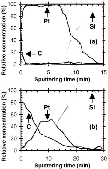
Figure 1a shows an Auger electron spectroscopy~AES! depth profile of a 50 nm Pt thin film as deposited. As
ex-a!Electronic mail:[email protected]
pected, a smooth transition from the deposited layer to the substrate can be observed. In Figure 2b, the analyzed sample consists of a 20mm320mm structure exposed with the elec-tron beam. The line dose used to produce the square was 17
mC/cm. The surface of the sample is contaminated with car-bon which originates in the SEM chamber. A plateau can be observed corresponding to a Pt2Si region. From this
spec-trum it is clear that the heating effect of the focused electron beam is sufficient to enable the diffusion of silicon through the metal layer18 and form platinum silicide which has a slower etch rate than pure Pt. This difference in etch rates provides a means by which to pattern the metal layer with submicron resolution.
The formation of the silicide depends on several factors. The thickness of the deposited metal layer determines the values of the electron accelerating voltage to be used. Better results have been observed when the maximum dissipated energy of the electrons occurs in the metal layer near the junction with silicon. Another important factor that deter-mines the temperature rise is the current density. Experi-ments have been carried out with a tungsten filament and the current density is approximately 100 mA/cm2 for a 1 keV electron beam.19 This value decreases slightly for currents less than 100 pA. Also, the current density increases with the electron beam energy due to the smaller probe size. A higher
current density increases the heating at the interface. The last parameter that influences the silicide formation is the elec-tron beam exposure time or the line dose. A threshold line dose is required to form the silicide; when the exposure is less than the threshold value, the pattern will not resist the wet etching.
Figure 2 shows the threshold line dose versus the num-ber of repeated single line exposures. The experimental pa-rameters are as follows: 1 keV electron beam, 100 pA cur-rent and a 20 nm Pt film. We obtain the threshold line dose from the minimum total exposure required to form a continu-ous silicide line after etching. In order to reduce the carbon contamination and the local charging effects, the complete dose was achieved by multiple line exposures. The effect of carbon contamination is to absorb some of the electron en-ergy, thus reducing the amount of energy lost in the metal layer and decreasing the temperature rise. This technique of multiple exposure reduces the total line dose required for threshold by reducing the rate of carbon deposition.20 From Figure 2 it is seen that the total minimum dose is around 1.2
mC/cm and is obtained with more that seven exposures. Mul-tiple repetition also significantly decreases the linewidth at the threshold. For a given line dose, multiple repetition im-plies a series of shorter exposure times for the pattern. In this case, the temperature required for silicide formation may only be attained in the center of the beam due to its gaussian profile, thus creating the silicide in a region that is narrower than the beam diameter. When using a 3 keV electron beam under the same conditions, the undesirable effect of carbon contamination should be reduced. Carbon deposition is still present, but at 3 keV the energy loss by the primary electrons in the carbon layer will be less significant. This implies a reduction in the number of multiple exposures required to obtain the threshold dose.
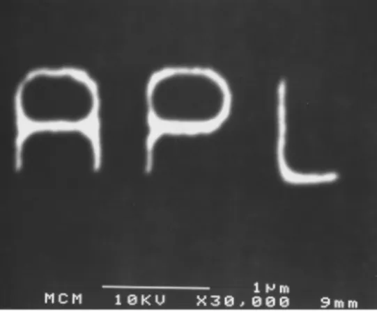
As an example, Figure 3 shows a nanostructure fabri-cated with this technique. The letters are about 1 mm in height and some lines have widths of less than 50 nm. The experimental conditions used in this case are 100 pA electron beam ('200 mA/cm2), 1.5mC/cm dose and 3 keV acceler-ating voltage.
After wet etching, the unexposed area may still be
con-FIG. 1. Auger electron spectroscopy depth profile of 50 nm of Pt on a silicon substrate.~a! As deposited and ~b! annealed with the electron beam.
FIG. 2. Threshold line dose and linewidth vs the number of repeated single line exposures.
3021
taminated with Pt. In fact, the first few nanometers of evapo-rated Pt can react with silicon at room temperature to form a silicide of about 2 nm ~Ref. 21! in thickness, thereby de-creasing the surface resistivity of the silicon. The surface resistivity in the unexposed area was restored to its original value by using a second etch step consisting of 6 minutes in H2O:HNO3:HF550:49:1. Also, to remove the surface
car-bon contamination due to the prolonged beam exposure in the SEM chamber, the surface can be exposed to an oxygen plasma etch for 20 minutes.
Proximity effects are reduced dramatically with this method. In fact, proximity effects with this process were ob-served only within the range of the electron beam diameter. So, by using a high performance SEM ~for example a field emission gun!, the beam diameter will be reduced and the current density will be increased. A finer structure with rela-tively insignificant proximity effects will then be achievable using an even smaller line dose.
A second important point to note is that no liftoff is required here unlike the case of resist-based processes. Such lift-off processes can significantly reduce resolution and re-duce the yield.
In summary, we have presented here a novel resistless fabrication technique to produce sub-50 nm metallic lines for
use as thin conducting structures or even as etching masks on silicon substrates. This process should reduce the proximity effects present in resist-based lithography, and while the resolution limit has not been determined clearly, it should be superior to the 50 nm linewidth obtained using a tungsten filament SEM.
Part of this research was funded by the Natural Sciences and Engineering Research Council of Canada~NSERC! and one of the authors~D.D.! would like to acknowledge support from NSERC.
1S. P. Beaumont, P. G. Bower, T. Tamamura, and C. D. W. Wilkinson,
Appl. Phys. Lett. 38, 438~1991!.
2W. Chen and H. Ohmed, J. Vac. Sci. Technol. B 11, 2519~1993!. 3D. Wang, P. C. Hoyle, J. R. A Cleaver, G. A. Porkolab, and N. C.
Mac-Donald, J. Vac. Sci. Technol. B 13, 1984~1995!.
4H. Sugimura and N. Nakagiri, J. Vac. Sci. Technol. B 13, 1933~1995!. 5C. A. Chang, J. Appl. Phys. 58, 3258~1985!.
6C. A. Chang and A. Segmuller, J. Appl. Phys. 61, 201~1987!. 7
C. A. Chang and W. K. Chu, Appl. Phys. Lett. 37, 3258~1980!.
8
C. A. Chang and J. M. Poate, Appl. Phys. Lett. 36, 417~1980!.
9C. A. Dimitriadis, Appl. Phys. Lett. 56, 143~1990!.
10A. Torres, S. Kolodinski, R. A. Donaton, K. Roussel, and H. Bender, Proc.
SPIE 2554, 185~1995!.
11
J. M. Poate and J. W. Mayer, Laser Annealing of Semiconductors ~Aca-demic, New York, 1982!.
12J. Narayan, W. L. Brown, and R. A. Lemons, Laser-Solids Interactions
and Transient Processing of Materials~North-Holland, New York, 1983!.
13
E. D’Anna, G. Leggieri, and A. Luches, Thin Solid Films 129, 93~1985!.
14
S. M. Sze, Physics of Semiconductor Devices, 2nd ed.~Wiley, New York, 1990!.
15E. G. Colgan, J. Mater. Res. 10, 1953~1995!.
16M. Yasuda, H. Kawata, K. Murata, K. Hashimoto, Y. Hirai, and N.
No-mura, J. Vac. Sci. Technol. B 12, 1362~1994!.
17Nanometer Pattern Generation System ver. 7.5, by JC Nabity Lithography
Systems, P.O. Box 5354, Bozeman, MT 59717.
18R. Pretaurius, M. A. E. Wandt, and J. E. McLeod, J. Electrochem. Soc.
136, 839~1989!.
19
J. I. Goldstein, D. E. Newbury, P. Echlin, D. C. Joy, A. D. Romig, Jr., C. E. Lyman, C. Fiori, and E. Lifshin, Scanning Electron Microscopy and X-Ray Microanalysis, 2nd ed.~Plenum, New York, 1994!, p. 820.
20J. Fujita, H. Watanabe, Y. Ochiai, S. Manako, J. S. Tsai, and S. Matsui,
Appl. Phys. Lett. 66, 3065~1995!.
21L. Ley, Y. Wang, V. Nguyen Van, S. Fisson, D. Souche, G. Vuye, and J.
Rivory, Thin Solid Films 270, 561~1995!. FIG. 3. SEM micrograph of a microstructure.