Resistless electron beam lithography process for the fabrication
of sub-50 nm silicide structures
D. Drouina)
De´partement de Ge´nie Me´canique, Groupe de Recherche sur les Mate´riaux pour Composants et Microstructures, Universite´ de Sherbrooke, Sherbrooke, Que´bec J1K 2R1, Canada
J. Beauvais, E. Lavalle´e, S. Michel, and J. Mouine
De´partement de Ge´nie E´ lectrique et de Ge´nie Informatique, Groupe de Recherche sur les Mate´riaux pour Composants et Microstructures, Universite´ de Sherbrooke, Sherbrooke, Que´bec J1K 2R1, Canada R. Gauvin
De´partement de Ge´nie Me´canique, Universite´ de Sherbrooke, Sherbrooke, Que´bec J1K 2R1, Canada ~Received 27 May 1997; accepted 21 July 1997!
We report on a study of the fabrication of submicron silicide structures with a resistless lithography technique. Several different metals can be used as a basis for producing silicide using this method; in this work, results will be discussed for both platinum and nickel silicide. The feasibility of producing nanostructures using polycrystalline silicon as a base growth layer for metal–oxide– semiconductor, and other device applications have also been demonstrated. Threshold doses for this method for submicron lines ~,50 nm! and square areas were obtained in order to establish a framework for the fabrication of more complex devices. Preliminary electrical measurements were carried out which indicate that the resistivity of the silicide is 45mV cm, and that the barrier height of the silicide/~high resistivity silicon! interface is 0.56 eV. © 1997 American Vacuum Society. @S0734-211X~97!01506-0#
I. INTRODUCTION
The continual reduction in size of microelectronic circuits and devices pushes the limits of current lithography pro-cesses. Several new techniques are presently under investigation,1,2 particularly for the fabrication of ultrasmall devices, in the sub-100 nm size domain. One of the main focus points of these activities is the development of a resist-less lithography process based on the use of an electron beam ~EB!. Several disadvantages are associated with the use of conventional resists in standard EB lithography. These in-clude proximity effects and resolution limits imposed by the size of the resist molecule. Therefore, several research groups have proposed methods by which chemical reactions can be activated by an EB, allowing for extremely high reso-lution often without any proximity effects.3,4 However the drawback is often the requirement that the EB exposure must be carried out in a reactive atmosphere in the sample chamber.5Recently, our group has proposed a method for a resistless EB lithography without the use of reactive gases.6 The EB is used to provide local heating of a thin metal film on a silicon substrate, thus generating silicide structures in the exposed areas. This method does not appear to suffer from the usual problems associated with resist based pro-cesses. Furthermore, the type of metal thin film that can be used includes all the metals that can form silicides at reason-ably low temperatures. In this article, we will discuss the formation of both platinum and nickel silicide structures us-ing this lithography process. In addition to metal– semiconductor structures~MESs!, the technique has been ex-tended to the fabrication of silicide structures over oxide
layers, using a thin layer of polycrystalline silicon covered with a metal thin film in order to produce the silicide layers. Thus, several types of structures were produced that can be used in the fabrication of metal–oxide–semiconductor ~MOS! devices. The results presented here will include a study of threshold exposure doses required for the fabrica-tion of both submicron lines and micrometer sized squares, and a comparison of the thresholds measured for platinum and nickel silicide structures. The effects of the beam energy will also be presented. Electrical measurements will also be discussed for both the MES and MOS structures fabricated using this lithography technique.
II. DESCRIPTION OF THE METHOD
Silicide structures are widely used in the microelectronics industry, due to the exceptionally good interface with silicon. Platinum silicide formed on n-type silicon produces a Schottky contact with a high barrier height (fb.0.8 eV!7
and is used, e.g., in bipolar integrated circuits.8 Silicide formed on p-type silicon generates a low barrier (fb,0.25
eV!7that can be used to fabricate infrared detectors.9These contacts are also widely used in MOS technology for low resistivity ohmic contacts.10 The formation of the metal– silicon compound is carried out by thermally activating the diffusion of the metal into the silicon. Usually this process is done in a conventional furnace in a controlled atmosphere of N2–H2.11 The process time using this technique to convert the metal layer into silicide is of the order of several minutes depending on the formation temperature. This process has been improved by the rapid thermal annealing ~RTA! tech-nique. The silicide formed by RTA is significantly better than that formed by conventional annealing, due to the a!Electronic mail: [email protected]
shorter processing time12and reduced contamination.10More recently, new techniques have been developed based on the principle of local heating of the interface between the metal and the silicon, rather than entire substrate heating.13 The thermal energy is due to energy transfer via the absorption of an EB at the surface. With this technique, an unfocused EB is used to anneal a previously patterned metal layer deposited on the substrate surface. The present work describes a differ-ent approach to directly pattern a metal layer deposited on a substrate.
Briefly, the present method produces an etch resistant structure from a metal/semiconductor interface. The process-ing steps include the deposition of a metal layer capable of reacting with the semiconductor, thermally activating the dif-fusion of the metal into the semiconductor with a focused EB, and producing the pattern of etch-resistant metal/ semiconductor compound by displacing the beam on the sur-face. This is followed by wet etching the undiffused layer of metal to leave only the etch-resistant metal/semiconductor compound on the semiconductor substrate.
More specifically, this work will study the formation of Pt and Ni alloys formed on a silicon substrate or a deposited polycrystalline Si layer. The formation of Pt silicide starts with the appearance of the Pt2Si compound in the tempera-ture range of 200–350 °C.14Once all the Pt is converted into Pt2Si and the temperature reaches the range of 300–450 °C,14 the growth of PtSi is initiated. In the case of nickel, the intermediate compounds are, in order, Ni2Si, NiSi, and NiSi2. The corresponding annealing temperatures are 200, 400, and 800 °C.15 In a previous article, the possi-bility of forming Pt2Si silicide layers using a standard scan-ning electron microscope ~SEM! has been demonstrated us-ing Auger electron spectroscopy characterization.6
In the present work we used a JEOL JSM-6300 SEM equipped with a standard tungsten hairpin filament and a beam blanker system. The EB is controlled using the NPGS16lithography software, which performs point by point exposures with blanking during beam displacement. The im-portant parameters are thus beam current, point separation, and exposure time for each point. To perform the heating of the thin metal layer, a small beam energy is usually used to insure that the maximum heating occurs near the metal/ semiconductor interface. An important problem associated with using a tungsten filament is the large electron probe size at low accelerating voltages. This large probe size limits the achievable temperature underneath the EB because the cur-rent density is not very large. Typically the probe diameter for a 1 keV, 100 pA EB is ;360 nm, which limits the at-tainable resolution. This lithography process could be en-hanced using a LaB6 or a field emission electron source, where typically the current density is increased by factors of 10 and 1000, respectively.
III. EXPERIMENTS
The objective of the present work is to establish the framework for the application of this method to the fabrica-tion of more complex devices such as MESFET or
MOSFET. Also, electrical characterization will be per-formed, to measure the conductivity of the silicide and the quality of the silicide/silicon interface.
Several types of samples were fabricated to fulfill these objectives. The first type ~type I! were intended to form a Schottky contact between the silicide and the silicon. A plati-num layer of 20 nm in thickness was evaporated on clean
n-type high resistivity silicon^100& substrates using an
elec-tron gun deposition system with an evaporation rate of 0.5 nm/s. Prior to this evaporation, P1 ions implantation at 40 keV was performed on the back of the samples, and annealed in a standard furnace at 950 °C in preparation for ohmic contacts.
The second type ~type II! of samples were fabricated to investigate the resistivity of the silicide and also the possi-bility of producing MOS capacitances. A 100-nm-thick ox-ide layer was first grown on a clean ^100& p-type silicon substrate in a furnace at 1050 °C. A 20 nm layer of polycrys-talline silicon is then deposited using low-pressure chemical vapor deposition ~LPCVD! at 620 °C. The final step is to evaporate a thin layer of Pt or Ni using the same conditions as described previously.
Type I platinum samples were used to investigate the ef-fect of the EB accelerating voltage. To perform this test, narrow lines of 20 mm in length were exposed with various line doses. The distance between each exposed point of the line was fixed at 3.4 nm and the beam current was set at 100 pA in this test, with only the point exposure time as a vari-able. The effect of repeated exposure was also investigated. This technique means that a single line is exposed more than one time. Area doses were studied using 2 mm32 mm squares. The effect of multiple exposure was once again amined as well as the variation of the distance between ex-posure points, in both cases with a fixed probe current. Using the same pattern, the difference in threshold doses for Pt and Ni silicide was determined. The threshold dose for an area is defined as the minimum dose to produce a complete defect-less square. For single lines the threshold dose is determined by the minimum dose required to form a continuous line. In the case of doses smaller than this threshold value, the lines include gaps.
In order to characterize the silicide/silicon junction, a 100
mm350 mm bonding pad was exposed with a dose of 240 mC/cm2 on Pt using a type I sample. The ohmic contacts were prepared using an Au–Sb eutectic alloy.
The final pattern used in this study is intended to measure the electrical resistivity of silicide structures produced with this lithography process. It consists of three parallel silicide lines connected to bonding pads. Geometrical considerations were used to calculate the resistivity of the structures.
After EB exposure, the unreacted metal layer is removed by wet chemical etching in an aqua region solution. The ratio of the acid constituents depends on the type of sample being etched. Table I presents a summary of the various recipes used in these experiments. Following the wet chemical etch-ing step, a thin layer of metal rich silicon remains on the surface of the samples. This is due to the formation, at room
temperature, of a very thin~'2 nm! silicide layer following metal evaporation at the metal–silicon interface.17In order to remove this layer and restore the initial surface conditions provided by the silicon substrate, type I samples are pro-cessed using a 3 min plasma etch in a CF4–O2gas mixture. Type II samples are also processed in the same fashion, but the plasma etch now removes the polycrystalline silicon layer outside of the silicide structures.
In the case of electrical measurements, reference samples were prepared using evaporation masks followed by conven-tional RTA.
IV. RESULTS AND DISCUSSION A. Exposure study
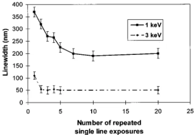
Figure 1 shows the threshold line dose versus the number of repeated single line exposures. The experimental param-eters are as follows: 1 and 3 keV EB, 100 pA current and a 20 nm Pt thin film on silicon. We obtain the threshold line dose from the minimum total exposure required to form a continuous silicide line after etching. In order to reduce the carbon contamination and the local charging effects, the complete dose was achieved by multiple line exposure. The effect of carbon contamination is to absorb some of the elec-tron energy, thus reducing the amount of energy lost in the metal layer and decreasing the temperature rise. This tech-nique of multiple exposure reduces the total line dose re-quired for reaching, threshold by reducing the rate of carbon deposition,3 due to the shorter exposure time of each point. From Fig. 1, it is seen that the total minimum dose is;1.2
mC/cm and is obtained with more than seven exposures.
When using a 3 keV EB under the same conditions, the undesirable effect of carbon contamination should be re-duced. Carbon deposition is still present, but at 3 keV the energy loss by the primary electrons in the carbon layer will be less significant due to the greater penetration depth of the electrons. This implies a reduction in the number of multiple exposures required to obtain the threshold dose as seen in Fig. 1, where the minimum dose is obtained after four expo-sures. Repeated line exposure also significantly decreases the linewidth at threshold, as shown in Fig. 2. For a given line dose, multiple exposure implies a series of shorter exposure times for the pattern. In this case, the temperature required for silicide formation may only be attained in the center of the beam due to its Gaussian profile, thus creating the silicide in a region which is narrower than the beam diameter. It is important to note that the effect of overetching the samples does not affect the measured linewidths. Increasing the EB energy, also significantly reduces the beam diameter and thus produces finer structure.18In fact, for a similar line dose at 1 and 3 keV, the line width at 3 keV is decreased by a factor of 5.
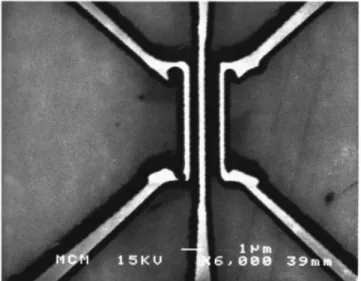
FIG. 3. Micrograph of silicide nanostructure. TABLEI. Etch parameters for different types of samples.
Sample type H2O–HCl–HNO3
Etch time~at 80 °C! ~min!
Pt on Si 8:7:1 4
Pt on poly-Si 22:7:1 7
Ni on Si 42:7:1 1
Ni on poly-Si 42:7:1 1
FIG. 1. Threshold, line dose as a function of the number of repeated single line exposures at 1 and 3 keV.
FIG. 2. Measured linewidth at threshold exposure dose as a function of the number of repeated single line exposures at 1 and 3 keV.
As an example, Fig. 3 shows a platinum silicide nano-structure fabricated with this technique. The letters are ;1
mm in height and some lines have widths ,50 nm. The experimental conditions used in this case are: 100 pA EB ~'200 mA/cm2), 1.5 mC/cm dose and 3 keV accelerating voltage. Under these conditions, the beam diameter is;250 nm. It is thus interesting to observe that within this figure, proximity effects are minimal and occur only at the junction of lines.
For area doses, the square pattern is exposed through a series of closely spaced horizontal lines. The distance be-tween each exposed line in this case is much less than the beam diameter. Thus, the effect of repeated exposures is not significant since this situation is always equivalent to a high number of repeated single line exposures.
Table II summarizes the results obtained by studying the effect of exposure point separation used in the square pat-terns for Pt samples. Normally, no effect should be observed because the area dose is independent of the point separation. The results of Table II shows some variation, but this is within the experimental errors.
A second metal, nickel, has also been studied. Since the previously studied effects should not be influenced by the type of metal, only the threshold doses should vary. Indeed, this parameter was measured to be four times greater than for the case of Pt thin film. This is related to a weaker resistance of nickel silicide to the chemical etching and different sili-cide formation temperature.
B. Electrical characterization
Figure 4 shows the forward and reverse current–voltage
relationship for a Pt/Si interface annealed with the SEM and by RTA. From the reverse saturation current the barrier height (fb) can be determined for both cases. These arefb
~SEM!50.56 eV and fb ~RTA!50.65 eV. The theoretical
value offbfor Pt silicide on high resistivity silicon is on the
order of 0.55 eV. Dimitriadis19 has shown that the method ~RTA or conventional furnace! and temperature of the anneal process has a strong influence on the obtained barrier height. In our experiments, the temperature used to anneal the samples is likely to be different by RTA and SEM annealing. While it is difficult to evaluate precisely the impact of the differences between the two techniques, these barrier height values are well within the range of values observed by Dimitriadis.19
In order to characterize a MOS structure, a similar contact pad used for Schottky measurements was exposed on a type II sample with a Pt layer to produce a MOS capacitance. In this case, the back ohmic contact was fabricated using alu-minum thin film deposition. Electrical measurement of the capacitance under zero bias revealed that the pad formed on the undoped polycrystalline silicon was indeed conductive, and a value of 20 pF was obtained.
The resistivity of the silicide produced with this method was determined using the structure illustrated in Fig. 5. This design was intended for multiple purposes: testing the fabri-cation of a structure containing closely spaced lines, verify-ing the interline electrical isolation and measurverify-ing the resis-tivity of the silicide structures. As shown in the example of Fig. 5, the line spacing is ,0.4 mm with linewidths of the same order. In addition to confirming the electrical isolation between the lines, the resistivity of the silicide was deter-mined to be;45mV cm. This value is reasonable since it is expected to be greater than the resistivity of pure platinum which is 10.6mV cm.
FIG. 4. Forward and reverse current–voltage relationship for a Pt/Si inter-face annealed with the SEM and by RTA.
FIG. 5. Micrograph of silicide nanostructure used for electrical measure-ments.
TABLEII. Effect of exposure point separation on area threshold dose. Point separation ~nm! Threshold dose ~mC/cm2) 3.4 65 7.0 40 14.0 46
V. SUMMARY
In this work, we have used a novel technique using a focused EB to generate silicide structures on a silicon sub-strate and a polycrystalline silicon thin film. Threshold, doses for lines and square areas have been obtained in order to establish a framework for the fabrication of more complex devices. While the resolution limit of this process has not been established, linewidths ,50 nm have been obtained. Preliminary electrical measurements have been carried out on silicide structures produced with this technique. This in-dicates that this method could be used in the fabrication of MES and MOS devices.
ACKNOWLEDGMENTS
Part of this research was funded by Micronet and the Natural Sciences and Engineering Research Council of Canada ~NSERC!. One of the authors ~D.D.! would like to acknowledge support from NSERC. They would also like to thank Jacques Corbin and Pierre Lafrance for technical sup-port.
1
D. Wang, P. C. Hoyle, J. R. A. Cleaver, G. A. Porkolab, and N. C. MacDonald, J. Vac. Sci. Technol. B 13, 1984~1995!.
2H. Sugimura and N. Nakagiri, J. Vac. Sci. Technol. B 13, 1933~1995!.
3J. Fujita, H. Watanabe, Y. Ochiai, S. Manako, J. S. Tsai, and S. Matsui, Appl. Phys. Lett. 66, 3065~1995!.
4W. Langheinrich and H. Beneking, Jpn. J. Appl. Phys., Part 1 32, 6248 ~1993!.
5H. Sugimura and N. Nakagiri, J. Vac. Sci. Technol. B 13, 1933~1995!. 6D. Drouin, J. Beauvais, R. Lemire, E. Lavalle´e, R. Gauvin, and M. Caron,
Appl. Phys. Lett. 70, 3020~1997!.
7W. E. Beadle, J. C. C. Tsai, and R. D. Plummer, Quick Reference Manual for Silicon Integrated Circuit Technology~Wiley, New York, 1985!. 8B.-Y. Tsaur, J. P. Mattia, and C. K. Chen, Appl. Phys. Lett. 57, 1111
~1990!.
9H. Bender, P. Roussel, S. Kolodinski, A. Torres, R. A. Donaton, K. Maex, and P. Vander Sluis, Mater. Res. Soc. Symp. Proc. 402, 449 ~1996!.
10C. A. Dimitrias, E. K. Polychroniadis, E. K. Evangelou, and G. E. Giak-oumakis, J. Appl. Phys. 70, 3109~1991!.
11B.-Y. Tsui and M.-C. Chen, J. Appl. Phys. 68, 6246~1990!.
12A. Torres, S. Kolodinski, R. A. Donaton, K. Roussel, and H. Bender, Proc. SPIE 2554, 185~1995!.
13
E. D’Anna, G. Leggieri, and A. Luches, Thin Solid Films 129, 93~1985!. 14E. G. Colgan, J. Mater. Res. 10, 1953~1995!.
15S. M. Sze, Physics of Semiconductor Devices, 2nd ed.~Wiley, New York, 1992!, p. 292.
16Nanometer Pattern Generation System ver. 7.5, by J. C. Nabity Lithogra-phy Systems.
17L. Ley, Y. Wang, V. Nguyen Van, S. Fisson, D. Souche, G. Vuye, and J. Rivory, Thin Solid Films 270, 561~1995!.
18P. Baumgartier, Appl. Phys. Lett. 64, 592~1994!. 19C. A. Dimitriadis, Appl. Phys. Lett. 56, 143~1990!.