HAL Id: hal-00488203
https://hal.archives-ouvertes.fr/hal-00488203
Submitted on 1 Jun 2010
HAL is a multi-disciplinary open access
archive for the deposit and dissemination of
sci-entific research documents, whether they are
pub-lished or not. The documents may come from
teaching and research institutions in France or
abroad, or from public or private research centers.
L’archive ouverte pluridisciplinaire HAL, est
destinée au dépôt et à la diffusion de documents
scientifiques de niveau recherche, publiés ou non,
émanant des établissements d’enseignement et de
recherche français ou étrangers, des laboratoires
publics ou privés.
1.55-µm optically pumped tunable VCSEL based on a
nano-polymer dispersive liquid crystal phase modulator
Christophe Levallois, Vivien Verbrugge, Laurent Dupont, Jean-Louis de
Bougrenet de la Tocnaye, Bertrand Caillaud, Alain Le Corre, Olivier Dehaese,
Hervé Folliot, Slimane Loualiche
To cite this version:
Christophe Levallois, Vivien Verbrugge, Laurent Dupont, Jean-Louis de Bougrenet de la Tocnaye,
Bertrand Caillaud, et al.. 1.55-µm optically pumped tunable VCSEL based on a nano-polymer
dis-persive liquid crystal phase modulator. Photonics Europe, Apr 2006, Strasbourg, France. pp.61850W,
�10.1117/12.662232�. �hal-00488203�
1.55-µm optically pumped tunable VCSEL based on a nano-polymer
dispersive liquid crystal phase modulator
C. Levallois
*a, V. Verbrugge
b, L. Dupont
b, J-L. de Bougrenet de la Tocnaye
b, B. Caillaud
b, A. Le
Corre
a, O. Dehaese
a, H. Folliot
a, S. Loualiche
aa
Laboratoire d ’Étude des Nanostructures à Semiconducteurs, UMR FOTON n°6082 - INSA
Rennes, 20 av. des Buttes de Coësmes, 35043 Rennes cedex, France.
b
ENST Bretagne, UMR FOTON n°6082 - Technopôle Brest-Iroise, CS 83818 - 29238 Brest Cedex,
France.
ABSTRACT
We present a new approach to achieve tunability on a 1.55 µm vertical cavity surface emitting laser (VCSEL). Tunability is achieved thanks to an electro-optic index modulator. This electro-optic material consists in a n-PDLC phase layer introduced inside the VCSEL cavity. N-PDLC comprises nematic liquid crystal dispersed in a polymer material. This first VCSEL exhibits a 10 nm tuning range and an excellent side-mode suppression ratio higher than 20 dB over the whole spectral range. The device is formed by a conventional InP-based active region with an epitaxial and a dielectric Bragg mirror. The n-PDLC layer length, close to 6 µm, is in agreement with a tunable laser emission without mode-hopping. Another decisive advantage, compared to mechanical solutions, is the tuning response time which is close to a few 10 µs to scan the full spectral range, making this device appropriate for some access network functions. Voltage values are the main limiting factor, 170 Volts have been required to obtain 10 nm tunability, but material engineering is in progress to improve this point. We presented a first version of the device optically pumped, the next version will be electrically pumped as required for access network applications targeted here.
Keywords: Tunable VCSEL, Polymer Dispersed Liquid Crystal, Optical pumping, Distributed Bragg Reflector, Electro-optical modulation
1.
INTRODUCTION
Long-wavelength vertical cavity surface emitting lasers (VCSEL) operating at 1.3 µm and 1.5 µm have been extensively studied during the last decade. Their circular and spatial single-mode beam provides very efficient fiber coupling and very attractive light sources for telecommunication. They also offer other advantages like wafer testing before packaging or fabrication in array configuration, well suited for low cost front end equipments of future Passive Optical Networks (PON). In order to increase communication capacities of the embedded fibers, advanced VCSELs with a tunable emission have been investigated.1 These kinds of devices make them suitable for wavelength division multiplexing (WDM) applications in metro and local access networks (MAN and LAN). Various solutions have been achieved such as microelectro-mechanical systems (MEMS) VCSEL2,3 and fiber Fabry-Perot surface emitting laser (FFPSEL).4 These vertical cavity tunable lasers exhibits promising performances according to the optical communication demand. Nevertheless, the FFPSEL needs complex mechanical alignments, although exhibiting very large wavelength tuning time, making them too expensive or not sufficiently reliable. Electrically or optically pumped VCSELs combined with MEMS technology offer an ideal solution for mode-hop free and wide wavelength tuning.5,6 However, this solution requires a complex processing and is limited by their fragility. Furthermore, MEMS technology exhibit a relatively low switching speed which depends of the MEMS structure size (few ms).5,7 An other way to obtain a wide VCSEL bandwidth is to use a liquid crystal as an electro-optic material placed inside the cavity.8 The liquid crystal (LC) solution allows to obtain a large refractive index variation, but the tuning speed is no faster than a millisecond and it also suffers from polarization dependence due to the birefringence of the nematic LC.
*
Many works demonstrated the advantages of nano-polymer dispersive liquid crystal (n-PDLC) compared with bulk LC or usual PDLC.9,10 This material is polarization insensitive and provide fast tuning speed which are interesting properties for a VCSEL. Thus, in this paper, we report the first tunable VCSEL operating in the C-band based on such a material. The device is easy to fabricate and robust. The VCSEL comprises a conventional InP based active region and an InP/InGaAsP bottom Bragg reflector. This half-cavity is combined with a SiO2/TiO2 front dielectric Bragg reflector
and the electro-optic phase modulator in order to tune the laser emission wavelength. This optically pumped VCSEL requires less than 170V to achieve a 10 nm tunability and presents a laser emission at room-temperature under pulsed-operation.
2.
TUNABLE VCSEL FABRICATION
2.1.Growth of the half-cavity
The first step to obtain the tunable VCSEL is the growth of a half cavity with a gas source molecular beam epitaxy (GS-MBE). This half cavity is grown in a single run, comprising InP/InGaAsP DBR and a periodic gain active region (Fig. 1). The cavity has an optical length of three half-wave periods which contains three sets of seven lattice-matched InGaAs/InGaAsP Quantum Wells (QW). Each multi-QWs (MQW) is located at an antinode of the standing wave for modal gain improvement. The thicknesses of the wells and barriers are 8 nm and 10 nm, respectively. Each set is surrounded by Q1.18 layers and InP layers (Q1.18 is a quaternary alloy In0.8Ga0.2As0.435P0.565 emitting at a 1.18 µ m
wavelength). The Q1.18 layers thicknesses which surrounds each MQW are optimized to obtain an homogenous optical
absorption of the pump power. This design allows to reach an homogenous carrier distribution for each QW. The growth of the bottom DBR is achieved with InP and Q1.45 semiconductor materials which are used as low and high
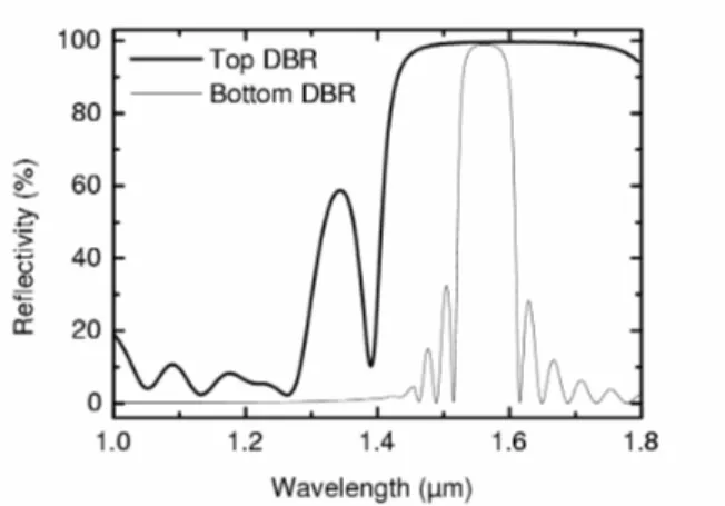
refractive index, respectively. The bottom DBR of the VCSEL is formed by 40 periods resulting in a theoretical reflectivity from cavity of 99% (Fig. 1). The thicknesses of each quarter-wavelength allow to match the resonant wavelength of the bottom mirror with the maximum optical gain of the QWs at 1.56 µ m. The high period number needed to reach this reflectivity implies to control the InP and Q1.45 layers thicknesses with an accuracy within 1%. As
illustrated in Fig. 1, the low refractive index between these two materials implies for our DBR a narrow spectral bandwidth. However, a calculated reflectance value higher than 98.5% can be hoped inside a spectral window greater than 30 nm centered around the resonant wavelength of the DBR. Thus, despite this low refractive index, the spectral window of the bottom DBR is in agreement with the tuning range targeted here.
Figure 1: Schematic cross-section of the tunable n-PDLC VCSEL. Figure 2: Measured reflectivity for the dielectric DBR deposited on glass substrate (thick line). Simulated reflectivity for semiconductor DBR (thin line).
2.2.Device assembling
A dielectric mirror is deposited on a glass substrate with an electron-beam evaporation system in order to obtain a front mirror as illustrated in Fig. 1. The use of dielectric materials for long wavelength VCSEL allows to obtain a high
reflectivity with a small number of periods.9,10 Here, we used silicon dioxide (SiO2) and titanium dioxide (TiO2)
material. The high index difference of ∆n = 0.8 between these two materials allows to reach a reflectivity of 99.5% at 1.55 µm with only 8.5 periods. Fig 2 depicts the measured reflectivity of the DBR for a normal incidence. As it is illustrated, the spectral bandwidth is larger than the semiconductor DBR and layers thicknesses used are optimized to minimize the reflectivity around 6% at 1.064 µm. Before the realization of this dielectric DBR, a thin semi-transparent electrode (ITO: Indium Tin Oxide) layer is deposited on the glass substrate in order to apply the electric field on the phase layer. The second electrode consists in a 200 nm gold layer on the back of the InP substrate. The InP substrate and the epitaxial layers are N-doped. Consequently, the major part of the electric field is applied on the n-PDLC phase layer and the dielectric DBR. Fig. 1 shows the final device where the half cavity and the front mirror are joined together thank to micrometric spacers. These micrometric spacers allow to obtain an air gap of 6 µm between the half cavity and the dielectric DBR with an accuracy to within 2%.
2.3.n-PDLC formation
At this stage, a device is realized but the electro-optic material is not introduced inside the device. Thus, the air-gap is filled with a mixture comprising nematic LC and UV-curable monomer. LC and the monomer were mixed at 30:70 wt% ratio. In order to realize photopolymerization-induced phase separation (PIPS) process,13 the mixture is UV cured through the Bragg mirror with strong UV illumination (λ = 365 nm - 350 mW/cm2) at room temperature (RT). Consequently, LC droplets are formed with a size close to 100 nm. This size is much smaller than the wavelength of the light used in optical-fiber communication systems. Therefore, the light is only slightly scattered by the droplets and the phase layer behaves as a pure refractive index modulator. Previously, the air-gap was measured to be 6 µm corresponding to an optical length of 6λ. The tuning layer and active region thicknesses were chosen in order to reach high enough gain for laser emission and a relatively large tuning range.
3.
N-PDLC INDEX MODULATOR DESCRIPTION
3.1.Refractive index variation
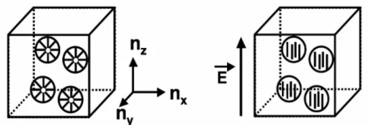
As we have seen, the tunable part of the device consists of a suspension of LC droplets in a host medium. The LC directors axes within a droplet are determined by the LC interaction at the droplet boundary and it is therefore vary nearly random from droplet to droplet in the absence of an external electric field E (Fig 3). As shown in Fig. 3, with an applied field along z, LC directors align parallel to E, causing index increase along z, whereas nx and ny decrease. For a
propagation vector k parallel to E, an incident light sees an index variation and the device operates as a pure polarisation insensitive variable phase delay.
Figure 3: Schematic representation of the n-PDLC material behaviour with and without an electric field.
For E and k collinear, the fraction of LC molecules aligned to the electric field can be estimated. Let us denote χLC the
weight fraction of LC in the cell, χAL the fraction of LC molecules aligned to E, and χPOL the weight fraction of polymer,
it is possible to express the average index as a function of the applied voltage by the following phenomenological expression:14
( )
E
LC AL( )
E
n
LC(
AL( )
E
)
n
LC POLn
POLn
=
χ
χ
⋅
0+
χ
1
−
χ
+
χ
(1)3
2
02 e2 LCn
n
n
=
+
(2)where LC birefringence ordinary index and extraordinary index are denoted n0 and ne respectively. The average
refraction index (for normally incident light) of the n-PDLC cell then changes with respect to the voltage by an amount of:
( )
E
( )(
E
n
n
0)
n
tot=
LC AL LC−
∆
χ
χ
(3)Thus, the applied bias voltage orients the droplets with respect to the induced electric field and creates a refractive index decrease.
3.2.n-PDLC absorption
n-PDLC exploits electro-optic properties of LC droplets. This approach is an interesting way to realize a tunable VCSEL because enabling more robust and compact solutions than with intra-cavity air gap modulation. However, optical losses of a such material must be weak because it is placed in a low gain high finesse VCSEL cavity. Furthermore, a large fraction of the intensity is located in the n-PDLC layer since its optical length is four times higher than the VCSEL active region. Thus, n-PDLC optical losses is a crucial parameter which implies important consequences on the lasing characteristics of the tunable VCSEL. Losses, such as scattering by the LC droplets must be minimized. The LC droplets diameter is dependant of the UV power used during PIPS process and have been estimated close to 100 nm in our case. Optical losses close to 15 cm-1 at 1.55 µm have been measured for specific samples comprising a n-PDLC layer sandwiched between two glass substrate. These optical losses are observed when LC droplets are randomly oriented without the application of the electric field.
3.3.Switching speed and driving voltage
n-PDLCs based-on LC droplets diameters close to 100 nm with respect to telecommunication wavelengths are also interesting because exhibiting faster response times than bulk LC. The switching speed is related to the droplet size, and it improves as the droplet size is reduced. In contrast, electro-optic forces needed to switch LC droplets are consequently much higher. Thus, the driving voltage is also dependant of the droplet size, and can be expressed as:15
D
C
V
d=
(4)where C is a constant and D is the droplet size. High voltage is required to switch LC directors (e.g. 20V/µm) in such a structure and this value is limited by the dielectric breakdown voltage. A decrease in droplet size reduces the response time but requires higher voltages to compensate the increase of elastic energy due strength in surface boundaries. But if an increase in droplet size decreases voltages it reduces the speed and introduces scattering losses. This is the common trade-off for such a material. If n-PDLC is polarisation insensitive and exhibits fast response times it requires high voltage values which limit its use in practice. However, various applications have been proposed using this material, such as for instance tunable Fabry-Perot filter16 or tunable focus microlens.17
4.
EXPERIMENTAL SET-UP
The photopumping experiment consists in focusing a laser beam with a microscope objective on the top mirror of the VCSEL with a spot area of 200 µm2. The laser emission is collected back by the same objective and transmitted through a beam splitter. The signal is injected in a large core diameter optical fiber connected to a spectrum analyzer. The photopumping of the active region is realized by a pulsed Q-switched YAG laser at a 1.064 µm wavelength. This laser produces 1 ns-long pulses at a repetition rate of 6.6 kHz. The pump beam propagates through an attenuating arrangement which allows pump power variations. A fraction of the incident beam is transmitted through the beam splitter in order to determine the average pump power behind the microscope objective.
Figure 4: The schematic of experimental set-up.
5.
EXPERIMENTAL RESULTS
5.1.Laser characterization and tunability
The average signal emitted by the VCSEL versus the average power of the pump for no applied voltage on the n-PDLC layer is reported in Fig. 5. A laser emission has been observed at RT with an emission wavelength of 1.56 µ m. This emission wavelength is in agreement with the maximum optical gain of the QWs and with the resonant wavelength of the bottom DBR. As it can been seen in Fig. 5, the average threshold power is close to 1 µW. The fraction of the incident pump radiation absorbed in the active region has been estimated using a transfer matrix based model of the VCSEL structure. At the pump wavelength the structure has a low reflectance but a fraction of the incident is not absorbed by the active region. Thus, we assume that only 40% of the incident pump power radiation is actually absorbed in the active region. In these conditions, the average pump power of 1 µW corresponds to a threshold power density of about 30 kW.cm-2. This threshold value is high but it can be explained by optical losses which are higher than the one expected. As mentioned above, the UV power used during PIPS process is a crucial parameter. The size of the LC droplets is dependant of the used UV power. In our case, a part of the incident UV power is absorbed by the SiO2/TiO2
dielectric Bragg mirror. Consequently the size of the LC droplets is probably higher than 100 nm which implies optical losses higher than 15 cm-1. But optical losses inside the electro-optic layer is not the only one factor. The experimental reflectance of the bottom DBR is may be lower than the one calculated and presented above.
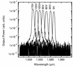
Fig. 6 shows emission spectra under constant optical pumping at different tuning voltage values. As the applied voltage between the top and bottom DBRs is increased from 0 to 170 V, the VCSEL wavelength is tuned from 1561.6 to 1551.8 nm. The increase of the applied voltage on the VCSEL reduces the refractive index of the n-PDLC layer and therefore shifts the laser emission to shorter wavelengths. A tuning range of 9.8 nm is then demonstrated with an applied voltage close to 170V. All the spectra presented in Fig. 2 have been recorded for a pump power level equal to one and a half time higher than the threshold pump power value at 0V. As illustrated in Fig. 6, we notice the good single mode operation of the VCSEL with side-modes which are rejected at more than 20dB for the whole tuning range. The free spectral range (FSR) which have been calculated is larger than 50 nm which is highly compatible with the observed tuning range of 10 nm. Consequently, the FSR is sufficient to eliminate mode hopping during wavelength tuning.
Figure 6: Wavelength shift for different tuning voltage. Tuning voltage are indicated above each peak, in volts.
Figure 7: Emission wavelength and output power of the VCSEL as a function of the applied voltage. The solid curve is the simulated wavelength variation for low tuning voltage.
The Fig. 7 depicts the wavelength tunable range as function of the voltage applied on the VCSEL structure. The wavelength decreases with a sigmoid behaviour when voltage increases and approaches saturation at around 150V. The tunability efficiency which can be defined as:
dV
d
T
eff=
λ
(5)where λ is the emission wavelength and V the applied voltage, is maximum in the middle of the sigmoid curve and is equal to 0.16 nm/V. The saturation tendency which occurs at high voltage means that the LC droplets become almost completely aligned in the direction of the electric field and the maximum index variation is reached. Considering our VCSEL structure, simulations based on transfer matrix calculations revealed that a 10 nm corresponds to a refractive index variation of ∆nmax = 1.5.10-2. This maximum refractive index variation can be expressed as:18
3
maxn
x
n
=
CL⋅
δ
∆
(6)where xCL is the fraction of LC in the polymer, δn equals here to 0.2 is the birefringence of LC. According to our
tunable range, the fraction of LC is 0.2. This concentration is lower than the one used to realize our n-PDLC material. This is because a portion of the LC material is dissolved in the polymer matrix and cannot be reoriented even in the high voltage regime. Thus, the effective LC concentration is smaller than the one expected. For weak voltage, the laser emission wavelength can be predicted with the use of the following expression:
2
E
n
=
⋅
∆
α
(7)where E is the electric field applied on the n-PDLC material (V/µ m) and α a constant of proportionality function of LC droplets size and density. As it can be seen in previous work,16 for low tuning voltage, a good agreement is obtained
between our experimental data and the laser peak wavelength calculated from this quadratic dependency of the refractive index with the electric field. The output power vs the laser emission wavelength is represented in Fig. 7. As the applied voltage between the top and bottom DBR is increased from 0 to 170V, the VCSEL output power increases of 3dB. This variation of the emitted power can be explained by the decrease of losses related to LC droplets scattering during the wavelength tuning. Experiments have been carried out with specific samples comprising a n-PDLC layer embedded between two glass substrate. A dependency of n-PDLC optical losses with the applied voltage have been revealed. When LC droplets are randomly oriented, the scattering losses inside the phase layer are higher than when the voltage is maximum and almost of the LC droplets are aligned with the applied electric field. Consequently, the estimated pump power threshold which have been determined in the above section is the highest when all the LC droplets directors are randomly oriented without voltage applied on the VCSEL.
5.2.PDL measurement
Another important factor is the polarization dependent loss (PDL). Because the polarization orientation of the emitted mode can change and the LC directors reorient as a function of the applied voltage, it is necessary to verify that the modulator does not impact significantly the polarization state, resulting in possible gain mismatch and wavelength drift. Randomly oriented LC droplets potentially prevent polarization dependence because the droplets are smaller than 100 nm, which is much smaller than the 1.55 µm wavelength. Furthermore, without electric field applied on this electro-optic material, LC droplets are randomly oriented, so a medium containing such droplets apparently becomes electro-optically isotropic to light in the infrared region. This hypothesis has been verified with the use of samples comprising a n-PDLC layer sandwiched between two glass substrate covered with ITO layers. UV power used during PIPS process and n-PDLC layer thickness are the same than the ones used for the VCSEL fabrication. Measurements have been carried out using Agilent 8509B Polarimeter. PDL introduced by the n-PDLC as a function of various applied voltages corresponding to various directors orientations is reported in Fig. 6. For all the applied voltage range, the PDL remains low, below 0.22 dB and the results presented previously on our tunable VCSEL are in agreement with this analysis.
Figure 8: Polarization dependant loss as a function of the applied voltage.
5.3.Tuning speed measurement
The VCSEL tuning response time is basically related to the electro-optic dynamics. Electro-optic response in N-PDLC are as fast as anchoring forces are strong (i.e. droplets are small). Typical switching responses of 100 µs are obtained with our material choice and LC concentration, therefore enabling wavelength shift over the whole range. However, as seen on Figure 7 only a limited voltage range close to 90 V is needed to scan 90% of the wavelength range. The response time of the transition between the no applied voltage and the steady states is greatly reduced when applying a large voltage pulse during a short laps of time prior to apply a steady state voltage.19 These pre-orientation pulses can be used to speed up significantly the material without damages. For instance, by using the addressing scheme presented in Fig 9, it is possible to speed up significantly the device. Short pre-pulses of 25 µ s are used to switch the LC rapidly, before applying the voltage value corresponding to the chosen wavelength to be addressed and so far, for another wavelength value.As it can be seen in Fig. 9, wavelengths can be tuned in less than 30µs, and the response time, for the considered voltage range, is not a function of the selected wavelength. Observation has been made possible by measuring the intensity variation at 633 nm due to scattering which depends on the proportion of oriented LC droplets
directors in our n-PDLC layer. As it was expected, the response time is speeded up by the high voltage value of the short pulse. Typical response times of 10 to 15 µs are expected with such a material choice and addressing scheme, making this solution advantageous compared to mechanical solutions.
Figure 9: Applied voltage and the measured response time of n-PDLC material.
6.
CONCLUSION
In conclusion, we demonstrated the first laser emission for a wavelength tunable 1.55 µm VCSEL in which wavelength tuning is obtained via an electric field induced index modulation of a n-PDLC layer. First characterizations have shown a tuning range equal to 10 nm under 170V applied voltage. This preliminary demonstration has been achieved with an optical pumping. The device is easy to realize and do not need complex processing as in MEMS VCSEL. The preliminary switching times measurements shown that any wavelength can be selected in less than 30 µs. The use of a more efficient bottom DBR and smaller LC droplets will improve pump power near the threshold in order to develop an electrically pumped VCSEL. Finally, the high voltage value can be reduced by employing and introducing ITO electrodes with low optical losses inside the cavity, close to the n-PDLC layer.
ACKNOWLEDGMENT
The authors wish to acknowledge the Brittany region for supporting this project and the Kerdry company for manufacturing the dielectric Bragg mirrors. The authors also wish to thank P. Gautier from Optogone for fruitful discussions about the optimization of the UV curing process.
REFERENCES
1. C. J. Chang-Hasnain, "Tunable VCSEL", IEEE J. Select. Topics in Quantum Electron., 6, pp. 978-987, 2000. 2. A. Tarraf, F. Riemenschneider, M. Strassner, J. Daleiden, S. Irmer, H. Halbritter, H. Hillmer, and P. Meissner,
"Continuously tunable 1.55-µm VCSEL implemented by precisely curved dielectric top DBR involving tailored stress", IEEE Photon. Technol. Lett., 16, pp. 720-722, 2004.
3. J. Boucart, R. Pathak, D. Zhang, M. Beaudoin, P. Kner, D. Sun, R. J. Stone, R. F. Nabiev, and W. Yuen, "Long wavelength MEMS tunable VCSEL With InP–InAlGaAs bottom DBR", IEEE Photon. Technol. Lett., 15, pp. 1186-1188, 2003.
4. K. Hsu, C. M. Miller, D. Babic, D. Houng, and Adrian Taylor, "Continuously tunable photopumped 1.3-µ m fiber fabry–perot surface-emitting lasers", IEEE Photon. Technol. Lett., 10, pp. 1199-1201, 1998.
5. F. Riemenschneider, M. Maute, H. Halbritter, G. Boehm, M.-C. Amann, and P. Meissner, "Continuously tunable long-Wavelength MEMS-VCSEL with over 40-nm tuning range", IEEE Photon. Technol. Lett., 16, pp. 2212-2214, 2004.
6. D. Vakhshoori, P. Tayebati, C.C. Lu, M. Azimi, P. Wang, J.H. Zhou and E. Canoglu, "2 mW CW singlemode operation of a tunable 1550-nm VCSEL with 50-nm tuning range", Electron. Lett., 35, pp. 900-901, 1999. 7. J. D. Berger, Y. Zhang, J. D. Grade, H. Lee, S. Hrinya, and H. Jerman, "Widely tunable external cavity diode laser
based on a MEMS electrostatic rotary actuator", Optical Fiber Communication Conference (OFC), Anaheim-California, March 2001.
8. N. K. Dutta, and D. Vakhshoori, “Article comprising a tunable semiconductor laser”, US patent n°5301201, 1994. 9. S. Matsumoto, M. Houlbert, Takayoshi, and K.-ichi Kubodera, "Fine droplets of liquid crystals in a transparent
polymer and their response to an electric field", Appl. Phys. Lett., 69, pp. 1044-1046, 1996.
10. P. J. W. Hands, A.K. Kirby, and G.D. Love, "Phase modulation with polymer-dispersed Liq. crystals" Proceedings of the SPIE, 5894, August 2005.
11. C. Levallois, A. Le Corre, S. Loualiche, O. Dehaese, H. Folliot, C. Paranthoen, F. Thoumyre, and C. Labbé, "Si wafer bonded of a-Si/a-SiNx distributed Bragg reflectors for 1.55-µm wavelength vertical cavity surface emitting
lasers", J. Appl. Phys., 98, pp. 043107, 2005.
12. J. Kinoshita, T. Miyamoto, Y. Onishi, and Fumio Koyama, "Characterization of single-wavelength optically pumped GaInAsP/InP vertical-cavity surface-emitting lasers with dielectric mirrors", Jpn. J. Appl. Phys., 43, pp. 5928-5932, 2004.
13. L. Bouteiller, and P. Le Barny, "Polymer-dispersed liquid crystals: preparation, operation and application", Liq. Cryst., 21, pp. 157-74 , 1996.
14. J. L. de Bougrenet de la Tocnaye, “Engineering liquid crystal for optimal uses in optical communication environments”, Liq. Cryst., 31, pp. 1-29, 2004.
15. H. Ren, and S.-T. Wu, "Inhomogeneous nanoscale polymer-dispersed liquid crystals with gradient refractive index", Appl. Phys. Lett., 81, pp. 3537-3539, 2002.
16. S. Matsumoto, H. Hirabayashi, S. Sakata, and T. Hayashi, “Tunable wavelength filter using nano-sized droplets of liquid crystal”, IEEE Photon. Technol. Lett., 11, pp. 441-444, 1999.
17. H. Ren, Y.-H. Fan, Y.-H. Lin, S.-T. Wu, "Tunable-focus microlens arrays using nanosized polymer-dispersed liquid crystal droplets", Optics Comm., 247, pp. 101-106, 2005.
18. V. Verbrugge, J.-L. de Bougrenet de la Tocnaye, and L. Dupont, "C-band wavelength-tunable vertical-cavity laser using a nano polymer dispersed liquid crystal material", Optics Comm., 215, pp. 353-359, 2003.