Applications des technologies mémoires MRAM appliquées aux processeurs embarqués
347
0
0
Texte intégral
(2) Délivré par UNIVERSITÉ MONTPELLIER 2. Préparée au sein de l’école doctorale. Information, Structures et Systèmes Et de l’unité de recherche LIRMM Spécialité : Systèmes Automatiques et Microélectronique. Présentée par Luís Vitório Cargnini. Applications des technologies mémoires MRAM Appliquées aux processeurs embarqués. Soutenue le 12/11/2013 devant le jury composé de. Dr. Lionel TORRES. Professeur, Université Montpellier 2. Directeur de Thèse. Dr. Gilles SASSATELLI. Directeur de Recherche CNRS, LIRMM UMR CNRS 5506. Co-Encadrant. Dr. Guy Gogniat. Professeur, Université Bretagne-Sud, Lorient. Rapporteur. Dr. Bertrand GRANADO. Professeur, Université Pierre et Marie Curie, Paris. Rapporteur. Dr. Jacques-Olivier Klein. Professeur, Université Paris Sud 11, Paris. Président. Dr. Daniel Étiemble. Professeur, Université Paris Sud 11, Paris. Examinateur. Dr. Guillaume Prenat. Ingénieur-Docteur, CEA, Laboratoire SPINTEC, Grenoble. Examinateur.
(3) Académie de Montpellier. U n i v e r s i t é M o n t p e l l i e r II. — Sciences et Techniques du Languedoc —. Thèse présentée au Laboratoire d’Informatique de Robotique et de Microélectronique de Montpellier pour obtenir le grade de. Docteur de l’Université Montpellier II Discipline. :. Génie Informatique, Automatique et Traitement du Signal. Formation Doctorale. :. Systèmes Automatiques et Microélectronique. École Doctorale. :. Information, Structures et Systèmes. MRAM APPLIED TO EMBEDDED PROCESSORS ARCHITECTURE AND MEMORY HIERARCHY NON-VOLATILE MEMORY MRAM INTO THE MEMORY HIERARCHY par. Luís Vitório Cargnini. Jury composé de : Lionel Torres. Professeur, Université Montpellier II/CNRS, Montpellier, France. Directeur de thèse. Gilles Sassatelli. Directeur de recherche/CNRS, Montpellier, France. Co-encadrant. Guy Gogniat. Professeur, Université de Bretagne Sud, Lorient, France. Rapporteur. Bertrand Granado. Professeur, Université Pierre et Marie Curie, Paris, France. Rapporteur. Jacques-Olivier Klein. Professeur, Institut d’Électronique Fondamentale, Université Paris Sud 11, Paris, France. Président. Daniel Étiemble. Professeur, Lab. de Recherche en Informatique, Université Paris Sud 11, Paris, France. Examinateur. Guillaume Prenat. Ingenieur, CEA Spintec, Grenoble, France. Examinateur.
(4)
(5) luís vitório cargnini MRAM APPLIED TO EMBEDDED PROCESSORS ARCHITECTURE A N D M E M O RY H I E R A R C H Y.
(6)
(7) MRAM APPLIED TO EMBEDDED PROCESSORS ARCHITECTURE AND M E M O RY H I E RA R C H Y luís vitório cargnini. Non-volatile Memory MRAM into the memory hierarchy Ph.D. I2S LIRMM – Laboratoire d’Informatique, de Robotique et de Microélectronique de Montpellier Université de Montpellier 2 November 12, 2013 – version 7.3.
(8) Luís Vitório Cargnini: MRAM applied to Embedded Processors architecture and Memory Hierc , November archy , Non-volatile Memory MRAM into the memory hierarchy , Ph.D., 12, 2013 supervisors: Lionel Torres Gilles Sassatelli location & time frame: Montpellier,France, November 12, 2013.
(9) To my wife, that endured, my years of Ph.D., my absences. I was lucky to have found you at our Alma Mater ! Thanks for all the trust, help and support you give me everyday, we finally can go home ! To my thesis baby: now, dad have time to play !. New ideas pass through three periods: 1) It can’t be done. 2) It probably can be done, but it’s not worth doing. 3) I knew it was a good idea all along! Arthur C. Clarke Ohana means family. Family means nobody gets left behind, or forgotten. — Lilo & Stitch. Ad Verum Ducit — Pontifícia Universidade Católica do Rio Grande do Sul (PUCRS) motto..
(10)
(11) ABSTRACT. The Semiconductors Industry with the advent of submicronic manufacturing flows below 45nm began to face new challenges to keep evolving according with the Moore’s Law. Regarding the widespread adoption of embedded systems one major constraint became power consumption of Integrated Circuit (IC). Also, memory technologies like the current standard of integrated memory technology for memory hierarchy, the SRAM, or the FLASH for non-volatile storage have extreme intricate constraints to be able to yield memory arrays at technological nodes below 45nm. One important is up until now Non-Volatile Memory weren’t adopted into the memory hierarchy, due to its density and like flash the necessity of multi-voltage operation. This thesis has the objective to work into these constraints and provide some answers. Into the thesis will be presented methods and results extracted from this methods to corroborate our goal of delineate a roadmap to adopt a new memory technology, non-volatile, low-power, low-leakage, SEU/MEU-resistant, scalable and with similar performance as the current SRAM, physically equivalent to SRAM, or even better with a area density between 4 to 8 times the area of a SRAM cell, without the necessity of multi-voltage domain like FLASH. This memory is the MRAM (Magnetic Memory), according with the ITRS one candidate to replace SRAM in the near future. MRAM instead of storing charge, they store the magnetic orientation provided by the spin-torque orientation of the free-layer alloy in the Magnetic Tunnel Junction (MTJ). Spin is a quantical state of matter, that in some metallic materials can have the orientation or its torque switched applying a polarized current in the sense of the desired field orientation. Once the magnetic field orientation is set, using a sense amplifier, and a current flow through the MTJ, the memory cell element of MRAM, it is possible to measure the orientation given the resistance variation, higher the resistance lower the passing current, the sense will identify a logic zero, lower the resistance the SA will sense a one logic. So the information is not a charge stored, instead it is a magnetic field orientation, reason why it is not affected by SEU or MEU caused due to high energy particles. Also it is not due to voltages variations to change the memory cell content, trapping charges in a floating gate. Regarding the MRAM, this thesis has by objective address the following aspects: MRAM applied to memory Hierarchy: • By describing the current state of the art in MRAM design and use into memory hierarchy; • by providing an overview of a mechanism to mitigate the latency of writing into MRAM at the cache level (Principle to composite memory bank); • By analyzing power characteristics of a system based on MRAM on CACHE L1 and L2, using a dedicated evaluation flow • by proposing a methodology to infer a system power consumption, and performance. • and for last based into the memory banks analyzing a Composite Memory Bank, a simple description on how to generate a memory bank, with some compromise in power, but equivalent latency to the SRAM, that keeps similar performance.. ix.
(12)
(13) P U B L I C AT I O N S. Some ideas and figures have appeared previously in the following publications: book chapters Weisheng Zhao, Lionel Torres, Luís Vitório Cargnini, Raphael Martins Brum, Yue Zhang, Yoann Guillemenet, Gilles Sassatelli, Yahya Lakys, Jacques-Olivier Klein, Daniel Etiemble, Dafiné Ravelosona, Claude Chappert, "High Performance SoC Design Using Magnetic Logic and Memory", VLSI-SoC: Advanced Research for Systems on Chip, IFIP Advances in Information and Communication Technology, Volume 379, 2012, pp 1033, DOI: 10.1007/978-3-642-32770-4_2, Print ISBN 978-3-642-32769-8, Online ISBN 978-3642-32770-4, ISSN 1868-4238, Springer Berlin Heidelberg, http://link.springer.com/ chapter/10.1007%2F978-3-642-32770-4_2. international conferences Torres, L.; Brum, R.M.; Cargnini, L.V.; Sassatelli, G., "Trends on the application of emerging nonvolatile memory to processors and programmable devices," Circuits and Systems (ISCAS), 2013 IEEE International Symposium on , vol., no., pp.101,104, 19-23 May 2013, doi: 10.1109/ISCAS.2013.6571792, http://ieeexplore.ieee.org/stamp/stamp.jsp? tp=&arnumber=6571792&isnumber=6571764. Torres, L.; Brum, R.M.; Guillemenet, Y.; Sassatelli, G.; Cargnini, L.V., "Evaluation of hybrid MRAM/CMOS cells for reconfigurable computing," New Circuits and Systems Conference (NEWCAS), 2013 IEEE 11th International , vol., no., pp.1,6, 16-19 June 2013, doi: 10.1109/NEWCAS.2013.6573676, http://ieeexplore.ieee.org/stamp/stamp.jsp? tp=&arnumber=6573676&isnumber=6573561. Cargnini, Luis Vitorio; Torres, Lionel; Brum, Raphael Martins; Senni, Sophiane; Sassatelli, Gilles, "Embedded memory hierarchy exploration based on magnetic RAM," Faible Tension Faible Consommation (FTFC), 2013 IEEE , vol., no., pp.1,4, 20-21 June 2013, doi: 10.1109/FTFC.2013.6577780, http://ieeexplore.ieee.org/stamp/stamp.jsp? tp=&arnumber=6577780&isnumber=6577746. Weisheng Zhao, Lionel Torres, Yoann Guillemenet, Luís Vitório Cargnini, Yahya Lakys, Jacques-Olivier Klein, Dafine Ravelosona, Gilles Sassatelli, and Claude Chappert. 2011. Design of MRAM based logic circuits and its applications. In Proceedings of the 21st edition of the great lakes symposium on Great lakes symposium on VLSI (GLSVLSI’11). ACM, New York, NY, USA, 431-436., DOI: 10.1145/1973009.1973104, http://doi.acm. org/10.1145/1973009.1973104. Zhao, W.S.; Zhang, Y.; Lakys, Y.; Klein, J-O; Etiemble, D.; Revelosona, D.; Chappert, C.; Torres, L.; Cargnini, L.V.; Brum, R. M.; Guillemenet, Y.; Sassatelli, G., "Embedded MRAM for high-speed computing," VLSI and System-on-Chip (VLSI-SoC), 2011 IEEE/IFIP 19th International Conference on , vol., no., pp.37,42, 3-5 Oct. 2011, doi: 10.1109/VLSISoC.2011.6081627, http://dx.doi.org/10.1109/VLSISoC.2011.6081627. xi.
(14) Barthe, L.; Cargnini, L.V.; Benoit, P.; Torres, L., "The SecretBlaze: A Configurable and Cost-Effective Open-Source Soft-Core Processor," Parallel and Distributed Processing Workshops and Phd Forum (IPDPSW), 2011 IEEE International Symposium on , vol., no., pp.310,313, 16-20 May 2011, doi: 10.1109/IPDPS.2011.154, http://ieeexplore.ieee. org/stamp/stamp.jsp?tp=&arnumber=6008911&isnumber=6008799. Barthe, L.; Cargnini, L.V.; Benoit, P.; Torres, L., "Optimizing an Open-Source Processor for FPGAs: A Case Study," Field Programmable Logic and Applications (FPL), 2011 International Conference on , vol., no., pp.551,556, 5-7 Sept. 2011, doi: 10.1109/FPL.2011.107, http://dx.doi.org/10.1109/FPL.2011.107 – Nominated the 6th best papers of FPL 2011 – Cargnini, L.V.; Guillemenet, Y.; Torres, L.; Sassatelli, G., "Improving the Reliability of a FPGA Using Fault-Tolerance Mechanism Based on Magnetic Memory (MRAM)," Reconfigurable Computing and FPGAs (ReConFig), 2010 International Conference on , vol., no., pp.150,155, 13-15 Dec. 2010, doi: 10.1109/ReConFig.2010.10, http://ieeexplore. ieee.org/stamp/stamp.jsp?tp=&arnumber=5695297&isnumber=5695271. national conferences Luis Vitorio Cargnini, Raphael Martins Brum, Gilles Sassatelli, Lionel Torres, "Exploration of MRAM cache memory for embedded processors", GDR SoC-SiP, 2012, June 13-15, Paris, France Luís Vitório Cargnini, Raphael Brum, Yoann Guillemenet, Lionel Torres, Gilles Sassatelli, "Improving the Reliability of a FPGA using Fault-Tolerance Mechanism Based on Magnetic Memory (MRAM)", GDR SoC-SiP, 2011, June 15-17, Lyon, France. xii.
(15) ACKNOWLEDGMENTS. The limits of the possible can only be defined by going beyond them into the Impossible. — Arthur C. Clarke To my advisor Professor Dr. Lionel Torres, who have gave me the chance and opportunity to work in a fascinating field as MRAM. Thank you for your time and patience, to advise me all this years. To my co-advisor Dr. Gilles Sassatelli for his insights during my research about the best approaches to evaluate an architecture. To the reviewers of my thesis Professor Dr. Guy Gogniat and Professor Dr. Bertrand Granado, for having the time to read my manuscript and for gently accept being part of my thesis committee. To Professor Dr. Jacques-Olivier Klein, Professor Dr. Daniel Étiemble, and Dr. Guillaume Prenat to also accept being part of my thesis committee. To my research network, which I worked and co-authored with them my many thanks for their insights to Jacques-Olivier Klein, Daniel Étiemble, Weisheng Zhao and Claude Chappert. To professor Dr. Fernando Gehm Moraes (PUCRS), by his help providing me access to the Cadence Physical Synthesis and Characterization tools, so I could fulfill and enrich my research. Also, for all the help trough this years. To Raphael Garibotti, for daily opportunity on debating, discussing, exchanging ideas regarding both researches. Also, for the help on how to conduct the Integrated Circuit experiments, aggregating ideas to my research. To Raphael Brum, for all the help during this last years at LIRMM writing a paper with tight dead-lines or discussing about the MTJ technology base in our researches. To Marcelo Mandelli, to have saved me in the last minute when I needed a Mac to finish one the images of my thesis. To Agence Nationale de Recherche (ANR) through SPIN,MARS and European Union (MODERN) for funding my research. To Lorival Regis, who promptly and efficiently provided me all the technical resources that allowed me to conduct my research. To Cécile Lukasik , for always so kindly help and solve the administrative related issues. To God, that gave me strength, wisdom and perseverance all this years to conclude my Ph.D... xiii.
(16)
(17) CONTENTS. i introduction 1 introduction ii 2. state of the art, drafted methodologies and materials current state of memory technology 2.1 Memory Taxonomy . . . . . . . . . . . . . . . . . . . . . . . . . . . . . . . 2.2 Memory Devices . . . . . . . . . . . . . . . . . . . . . . . . . . . . . . . . . 2.2.1 Ferroelectric Memory . . . . . . . . . . . . . . . . . . . . . . . . . 2.2.1.1 Ferroelectric FET . . . . . . . . . . . . . . . . . . . . . . . 2.2.1.2 Ferroelectric Polarization ReRAM . . . . . . . . . . . . . 2.2.2 Nanoelectromechanical memory (NEMM) . . . . . . . . . . . . . 2.2.3 Redox Memory . . . . . . . . . . . . . . . . . . . . . . . . . . . . . 2.2.4 Mott Memory . . . . . . . . . . . . . . . . . . . . . . . . . . . . . . 2.2.5 Macromolecular Memory . . . . . . . . . . . . . . . . . . . . . . . 2.2.6 Molecular Memory . . . . . . . . . . . . . . . . . . . . . . . . . . . 2.2.6.1 Vertical Transistors . . . . . . . . . . . . . . . . . . . . . . 2.2.6.2 Two-terminal select devices (resistance-based memories) 2.2.6.3 Diode-type select devices . . . . . . . . . . . . . . . . . . 2.2.7 Resistive-Switch-type select devices . . . . . . . . . . . . . . . . . 2.2.7.1 MIT switch . . . . . . . . . . . . . . . . . . . . . . . . . . . 2.2.7.2 Threshold switch . . . . . . . . . . . . . . . . . . . . . . . 2.2.7.3 MIEC switch . . . . . . . . . . . . . . . . . . . . . . . . . . 2.2.7.4 2 Terminal Switches . . . . . . . . . . . . . . . . . . . . . 2.3 Magnetic Tunneling Junction (MTJ) . . . . . . . . . . . . . . . . . . . . . . 2.3.1 Tunnel Magnetoresistance (TMR) . . . . . . . . . . . . . . . . . . 2.3.2 Field Induced Magnetic Switching (FIMS) MRAMs . . . . . . . . 2.3.3 Thermally Assisted Switching (TAS) MRAMs . . . . . . . . . . . 2.3.4 Spin Transfer Torque (STT) RAMs . . . . . . . . . . . . . . . . . . 2.3.5 STT based Magnetic Tunnel Junction (STT-MTJ) . . . . . . . . . . 2.3.6 Planar and Perpendicular STT . . . . . . . . . . . . . . . . . . . . 2.4 Current state compared to the memory state of the art . . . . . . . . . . 2.5 Computer Architecture and Memory Hierarchy . . . . . . . . . . . . . . 2.5.1 Working Principles of the Memory Hierarchy . . . . . . . . . . . 2.6 CACHE Memories . . . . . . . . . . . . . . . . . . . . . . . . . . . . . . . . 2.6.1 Larger block size to reduce MISS rate . . . . . . . . . . . . . . . . 2.6.2 Bigger caches to reduce MISS rate . . . . . . . . . . . . . . . . . . 2.6.3 Higher associativity to reduce MISS rate . . . . . . . . . . . . . . 2.6.4 Multilevel caches to reduce MISS penalty . . . . . . . . . . . . . . 2.6.5 Giving priority to read misses over writes to reduce MISS penalty 2.6.6 Avoiding address translation during indexing of the cache to reduce HIT time . . . . . . . . . . . . . . . . . . . . . . . . . . . . 2.7 MRAM applied into Memory Hierarchy . . . . . . . . . . . . . . . . . . .. 1 3 9 11 17 19 19 19 19 20 20 21 22 22 23 24 24 25 25 25 25 26 27 29 29 32 32 33 33 36 37 38 40 41 41 41 41 41 42 42. xv.
(18) xvi. contents. iii analytical methodology flow 3 analytical methodology flow 3.1 CACTI: Integrated Memory Simulator . . . . . . . . . . . . . . . . . . . . 3.1.1 CACTI background . . . . . . . . . . . . . . . . . . . . . . . . . . 3.1.2 CACTI Thesaurus . . . . . . . . . . . . . . . . . . . . . . . . . . . 3.1.3 NUCA Modeling . . . . . . . . . . . . . . . . . . . . . . . . . . . . 3.2 NVSim . . . . . . . . . . . . . . . . . . . . . . . . . . . . . . . . . . . . . . 3.2.1 NVSim Non-Volatile Memory (NVM) Physical Mechanisms and Write Operations . . . . . . . . . . . . . . . . . . . . . . . . . . . . 3.2.2 NAND Flash . . . . . . . . . . . . . . . . . . . . . . . . . . . . . . 3.2.3 STT-RAM . . . . . . . . . . . . . . . . . . . . . . . . . . . . . . . . 3.2.4 PCRAM . . . . . . . . . . . . . . . . . . . . . . . . . . . . . . . . . 3.2.5 ReRAM . . . . . . . . . . . . . . . . . . . . . . . . . . . . . . . . . 3.2.6 Charge Pump . . . . . . . . . . . . . . . . . . . . . . . . . . . . . . 3.2.7 Write Endurance Issue . . . . . . . . . . . . . . . . . . . . . . . . . 3.2.8 Retention Time Issue . . . . . . . . . . . . . . . . . . . . . . . . . . 3.2.9 MOS-Accessed Structure Versus Cross-Point Structure . . . . . . 3.3 Comparison of NVSim to CACTI . . . . . . . . . . . . . . . . . . . . . . . 3.4 Reliability of the methodology base-line models . . . . . . . . . . . . . . 3.5 Methodology to Evaluate the Intrinsic aspects of MRAM compared to SRAM memories . . . . . . . . . . . . . . . . . . . . . . . . . . . . . . . . . 3.5.1 Memory models used in NVSim for analyses . . . . . . . . . . . 3.5.2 Intrinsic Analyses . . . . . . . . . . . . . . . . . . . . . . . . . . . 3.5.3 Intrinsic Analyses - Results . . . . . . . . . . . . . . . . . . . . . . 3.5.3.1 Memory banks of 45nm . . . . . . . . . . . . . . . . . . . 3.6 Methodology to Evaluate the aspects of MRAM into Memory Hierarchy 3.7 SimpleScalar . . . . . . . . . . . . . . . . . . . . . . . . . . . . . . . . . . . 3.8 Gem5 . . . . . . . . . . . . . . . . . . . . . . . . . . . . . . . . . . . . . . . 3.8.1 Simulation Capabilities . . . . . . . . . . . . . . . . . . . . . . . . 3.8.2 ISAs . . . . . . . . . . . . . . . . . . . . . . . . . . . . . . . . . . . 3.8.3 Execution Modes . . . . . . . . . . . . . . . . . . . . . . . . . . . . 3.8.4 CPU Models . . . . . . . . . . . . . . . . . . . . . . . . . . . . . . . 3.8.5 Interconnection Networks . . . . . . . . . . . . . . . . . . . . . . . 3.8.6 Devices . . . . . . . . . . . . . . . . . . . . . . . . . . . . . . . . . .. 47 49 49 50 51 52 52. iv analyses of embedded memory hierarchy 4 analyses of embedded memory hierarchy 4.1 Embedded MRAM for Processor Applications . . . . . . . . . . . . . . . 4.1.1 MRAM applications for the processor memory hierarchy . . . . 4.1.2 In-Depth Analysis: Case Study CJPEG . . . . . . . . . . . . . . . 4.2 Using Gem5 to evaluate the implications into memory hierarchy of L2 CACHE banks of significant sizes from 2GB down to 256KB. . . . . . . . 4.2.1 Recalibrating the Gem5 using the NVSim bank details. . . . . . . 4.2.2 Power Analysis based into the memory banks generated after the NVSim. . . . . . . . . . . . . . . . . . . . . . . . . . . . . . . . 4.3 Benchmarks used for evaluations . . . . . . . . . . . . . . . . . . . . . . .. 93 95 96 96 98. 53 53 53 53 54 54 54 55 55 55 56 57 58 58 62 62 87 89 90 90 90 90 90 91 91. 102 106 114 115.
(19) contents. 4.4. 4.5 v 5. Comparing a Microprocessor memory hierarchy, synthesized with MRAM and SRAM at 28nm . . . . . . . . . . . . . . . . . . . . . . . . . . . . . . . 116 4.4.1 OpenRISC Architecture . . . . . . . . . . . . . . . . . . . . . . . . 119 4.4.1.1 Memory Model . . . . . . . . . . . . . . . . . . . . . . . . 120 4.4.1.2 Memory Synchronize Instruction . . . . . . . . . . . . . . 121 4.4.1.3 Memory Management . . . . . . . . . . . . . . . . . . . . 121 4.4.2 MRAM Characterization using Liberty . . . . . . . . . . . . . . . 122 4.4.3 Synthesis Results . . . . . . . . . . . . . . . . . . . . . . . . . . . . 123 4.4.4 MRAM and Static Random Access Memory (SRAM) synthesis results . . . . . . . . . . . . . . . . . . . . . . . . . . . . . . . . . . 124 4.4.5 Assessments comparing the synthesis results of the two technolgies . . . . . . . . . . . . . . . . . . . . . . . . . . . . . . . . . . . . 125 The Composite Bank . . . . . . . . . . . . . . . . . . . . . . . . . . . . . . 127 4.5.1 Composite Memory banks of 45nm . . . . . . . . . . . . . . . . . 127. conclusions & future insights conclusions & future insights. vi appendix a mram terminology a.1 Anisotropy . . . . . . . . . . . . . . . . . . . . . . . . . . . . . . . . . . . . a.2 Magnetic anisotropy . . . . . . . . . . . . . . . . . . . . . . . . . . . . . . . a.3 Superparamagnetism . . . . . . . . . . . . . . . . . . . . . . . . . . . . . . a.4 Magnetic Permeability . . . . . . . . . . . . . . . . . . . . . . . . . . . . . a.5 Isotropy . . . . . . . . . . . . . . . . . . . . . . . . . . . . . . . . . . . . . . a.6 Magnetic moment . . . . . . . . . . . . . . . . . . . . . . . . . . . . . . . . a.7 Magnetic moment and angular momentum . . . . . . . . . . . . . . . . . a.8 Exchange bias . . . . . . . . . . . . . . . . . . . . . . . . . . . . . . . . . . a.9 Antiferromagnetism . . . . . . . . . . . . . . . . . . . . . . . . . . . . . . . a.9.1 Measurement . . . . . . . . . . . . . . . . . . . . . . . . . . . . . . a.9.2 Antiferromagnetic materials . . . . . . . . . . . . . . . . . . . . . a.9.3 Geometric frustration . . . . . . . . . . . . . . . . . . . . . . . . . b improving the reliability of a fpga using fault-tolerance mechanism based on mram b.1 Reliability . . . . . . . . . . . . . . . . . . . . . . . . . . . . . . . . . . . . . b.2 Mechanism to improve reliability regarding SEU events . . . . . . . . . . b.3 Scrubbing Mechanism - Refresh the configuration bits . . . . . . . . . . . b.4 General approach . . . . . . . . . . . . . . . . . . . . . . . . . . . . . . . . b.5 Error Detection Code . . . . . . . . . . . . . . . . . . . . . . . . . . . . . . b.6 Experimental Results . . . . . . . . . . . . . . . . . . . . . . . . . . . . . . b.7 Hamming results . . . . . . . . . . . . . . . . . . . . . . . . . . . . . . . . b.8 BCH Results . . . . . . . . . . . . . . . . . . . . . . . . . . . . . . . . . . . b.9 Assessments on MRAM applied to FPGA to improve reliability . . . . . c intrinsic analyses - additional results d cacti analytical models - relevant details d.1 CACTI Analytical Models . . . . . . . . . . . . . . . . . . . . . . . . . . . d.2 Wire Parasitics . . . . . . . . . . . . . . . . . . . . . . . . . . . . . . . . . .. 149 151 155 157 157 157 158 158 158 159 159 160 160 160 160 161 163 164 165 167 167 169 170 170 171 171 173 181 181 181. xvii.
(20) xviii. contents. e f. d.3 Global Wires . . . . . . . . . . . . . . . . . . . . d.4 Low-swing Wires . . . . . . . . . . . . . . . . . d.5 Transmitter . . . . . . . . . . . . . . . . . . . . . d.6 Sense Amplifier . . . . . . . . . . . . . . . . . . intrinsic analyses - memory banks of 28nm the composite bank - additional results f.1 LOP 45nm . . . . . . . . . . . . . . . . . . . . . f.2 Composite Baank 28nm . . . . . . . . . . . . . . f.3 LOP 28nm . . . . . . . . . . . . . . . . . . . . .. bibliography. . . . .. . . . .. . . . .. . . . .. . . . .. . . . .. . . . .. . . . .. . . . .. . . . .. . . . .. . . . .. . . . .. . . . .. . . . .. 181 183 183 184 185 205 . . . . . . . . . . . . . . . 205 . . . . . . . . . . . . . . . 225 . . . . . . . . . . . . . . . 245 265.
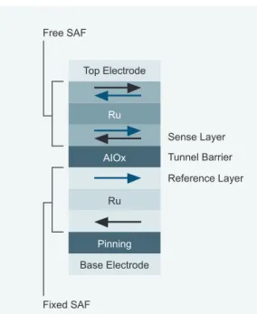
(21) LIST OF FIGURES. Figure 1.1 Figure 1.2 Figure 2.1 Figure 2.2. Figure 2.3. Figure 2.4. Figure 2.5. Figure 2.6 Figure 2.7 Figure 2.8 Figure 2.9. Figure 2.10 Figure 2.11. Figure 3.1 Figure 3.2 Figure 3.3. Relationship among More Moore, More-than-Moore, and Beyond CMOS [ITRS, 2012a]. . . . . . . . . . . . . . . . . . . . . . . . . . . . A Taxonomy for Emerging Research Information Processing Devices found in [ITRS, 2012a]. . . . . . . . . . . . . . . . . . . . . . . Physical difference between a vertical and a planar transistor, extracted from [Ou et al., 2010]. . . . . . . . . . . . . . . . . . . . . . . (a) MTJ structure and interconnection with the CMOS circuit and the relation of the MTJ according with the technology of anisotropy, (b) Planar MTJ, (c) Perpendicular MTJ. . . . . . . . . . . . . . . . . Schematic of a 1-transistor, 1-MTJ memory cell showing the write lines above and below the bit and the read current path [Everspin Technologies Inc., 2010]. . . . . . . . . . . . . . . . . . . . . . . . . . The magnetic tunnel junction (MTJ) material stack used for Toggle MRAM. The Free SAF magnetic moments switch between two states when the proper magnetic field sequence is applied. Electrons tunnel across the alumina (AlOx) tunnel barrier, resulting in a magnetoresistance that is sensitive to the magnetic moment direction of the sense layer [Everspin Technologies Inc., 2010]. . . Schematic of a toggle Magnetic Random Access Memory (MRAM) bit with the field sequence used to switch the free layer from one state to the other. The fields, H1, H1+H2 and H2 are produced by passing currents, i1 and i2, through the write lines [Everspin Technologies Inc., 2010]. . . . . . . . . . . . . . . . . . . . . . . . . . MTJ process to switch the electromagnetic thin-layer field and store the logic value into the MTJ passing from the electrical layer. High performance perpendicular MTJ with φ 40nm . . . . . . . . Microprocessor Datapath [Hennessy and Patterson, 2007b; Patterson and Hennessy, 2012]. . . . . . . . . . . . . . . . . . . . . . . . . The levels in a typical memory hierarchy in embedded and server computers. As we move further away from the processor, the memory in the lower level increases in latency and density. Note that the time units change by factors of 10, from picoseconds to milliseconds, and that the size units change by factors of 1000, from bytes to terabytes. . . . . . . . . . . . . . . . . . . . . . . . . . An example of a possible Set-Associative Cache Organization [Patterson and Hennessy, 2012]. . . . . . . . . . . . . . . . . . . . . . . A general overview of a hypothetical memory hierarchy going from virtual address to L2 cache access. [Hennessy and patterson, 2006] . . . . . . . . . . . . . . . . . . . . . . . . . . . . . . . . . . . . CACHE bank memory physical organization [Tarjan et al., 2006] . Evaluation Methodology depicted. . . . . . . . . . . . . . . . . . . Total Area. . . . . . . . . . . . . . . . . . . . . . . . . . . . . . . . . .. 4 7 23. 28. 30. 31. 31 32 35 38. 38 39. 42 50 57 67. xix.
(22) xx. List of Figures. Figure 3.4 Figure 3.5 Figure 3.6 Figure 3.7 Figure 3.8 Figure 3.9 Figure 3.10 Figure 3.11 Figure 3.12 Figure 3.13 Figure 3.14 Figure 3.15 Figure 3.16 Figure 3.17 Figure 3.18 Figure 3.19 Figure 3.20 Figure 3.21 Figure 3.22 Figure 3.23 Figure 4.1 Figure 4.2 Figure 4.3 Figure 4.4 Figure 4.5 Figure 4.6 Figure 4.7 Figure 4.8 Figure 4.9 Figure 4.10 Figure 4.11 Figure 4.12 Figure 4.13 Figure 4.14 Figure 4.15 Figure 4.16 Figure 4.17 Figure 4.18. CACHE Total Write Latency. . . . . . . . . . . . . . . . . . . . . . . CACHE DATA Array Leakage Power. . . . . . . . . . . . . . . . . . CACHE TAG Leakage Power. . . . . . . . . . . . . . . . . . . . . . Leakage Power. . . . . . . . . . . . . . . . . . . . . . . . . . . . . . . Low-Power (LOP) Total Leakage, observe only the Low Power Performance (LOP) banks observed in Figure 3.7. . . . . . . . . . . Hit Dynamic Energy. . . . . . . . . . . . . . . . . . . . . . . . . . . . Hit Latency. . . . . . . . . . . . . . . . . . . . . . . . . . . . . . . . . Miss Dynamic Energy. . . . . . . . . . . . . . . . . . . . . . . . . . . Miss Latency. . . . . . . . . . . . . . . . . . . . . . . . . . . . . . . . Data Read Latency. . . . . . . . . . . . . . . . . . . . . . . . . . . . . TAG Read Latency. . . . . . . . . . . . . . . . . . . . . . . . . . . . . DATA Write Latency. . . . . . . . . . . . . . . . . . . . . . . . . . . TAG Write Latency. . . . . . . . . . . . . . . . . . . . . . . . . . . . CACHE Write Dynamic Energy . . . . . . . . . . . . . . . . . . . . TAG Dynamic Energy . . . . . . . . . . . . . . . . . . . . . . . . . . TAG Write Latency . . . . . . . . . . . . . . . . . . . . . . . . . . . . Data Write Latency . . . . . . . . . . . . . . . . . . . . . . . . . . . . Write Bandwidth. . . . . . . . . . . . . . . . . . . . . . . . . . . . . Write Bandwidth. . . . . . . . . . . . . . . . . . . . . . . . . . . . . Evaluation Methodology depicted. . . . . . . . . . . . . . . . . . . Overview of the processor performance using low-capacity L1 caches. . . . . . . . . . . . . . . . . . . . . . . . . . . . . . . . . . . . Overview of the processor performance using high-capacity L1 caches. . . . . . . . . . . . . . . . . . . . . . . . . . . . . . . . . . . . Overview of Cycles Per Instruction (CPI) Penalty: best-case, worstcase and average of the Mediabench benchmarks’ performance. . Simulation results for 1000 cycles and 1 cycle of delay for each subsequent word in burst mode. . . . . . . . . . . . . . . . . . . . Simulation results for 1000 cycles and 10 cycles of delay for each subsequent word in burst mode. . . . . . . . . . . . . . . . . . . . % Miss Latency Encoder. . . . . . . . . . . . . . . . . . . . . . . . . % Miss Latency Decoder. . . . . . . . . . . . . . . . . . . . . . . . . Overall Miss Rate Encoder. . . . . . . . . . . . . . . . . . . . . . . . encoder L2 replacements. . . . . . . . . . . . . . . . . . . . . . . . . decoder L2 replacements. . . . . . . . . . . . . . . . . . . . . . . . . X.264 Execution time. . . . . . . . . . . . . . . . . . . . . . . . . . . X.264 Clock cycles. . . . . . . . . . . . . . . . . . . . . . . . . . . . . L2 Replacements. . . . . . . . . . . . . . . . . . . . . . . . . . . . . . L2 Overall Access Total. . . . . . . . . . . . . . . . . . . . . . . . . . L2 Overall Miss Latency. . . . . . . . . . . . . . . . . . . . . . . . . L2 ReadReq Access total. . . . . . . . . . . . . . . . . . . . . . . . . L2 Write Access Total. . . . . . . . . . . . . . . . . . . . . . . . . . . The OR1200 is a 32-bit scalar RISC with Harvard microarchitecture, 5 stage integer pipeline, virtual memory support (Memory Management Unit (MMU)) and basic Digital Signal Processing (DSP) capabilities. . . . . . . . . . . . . . . . . . . . . . . . . . . . .. 68 69 70 71 72 73 74 75 76 77 78 79 80 81 82 83 84 85 86 87 98 98 99 100 101 103 103 104 104 105 108 110 111 111 112 112 113. 119.
(23) List of Figures. Figure 4.19 Figure 4.20 Figure 4.21. Figure 4.22 Figure 4.23 Figure 4.24 Figure 4.25 Figure 4.26 Figure 4.27 Figure 4.28 Figure 4.29 Figure 4.30 Figure 4.31 Figure 4.32 Figure 4.33 Figure 4.34 Figure 4.35 Figure 4.36 Figure 4.37 Figure 4.38 Figure B.1 Figure B.2 Figure B.3. Figure B.4. Figure B.5 Figure D.1 Figure D.2 Figure E.1 Figure E.2 Figure E.3 Figure E.4 Figure E.5 Figure E.6 Figure E.7. Translation of Effective to Physical Address. Simplified block diagram for 32-bit processor implementations . . . . . . . . . . . . . . Synthesized OpenRISC architecture organization. . . . . . . . . . . Composite CACHE set bank architecture, built with two heterogeneous memory technologies. In the Figure the TAG(green matrix, left) is built using SRAM, while the DATA (blue matrix, right) is built using Spin Transfer Torque MRAM (STT-MRAM). . . . . . . Total Area. . . . . . . . . . . . . . . . . . . . . . . . . . . . . . . . . . Total Write Latency. . . . . . . . . . . . . . . . . . . . . . . . . . . . Composite Leakage Power. . . . . . . . . . . . . . . . . . . . . . . . Low-Power (LOP) Total Leakage, magnification on the LOP banks observed in Figure 4.24. . . . . . . . . . . . . . . . . . . . . . . . . . Hit Dynamic Energy. . . . . . . . . . . . . . . . . . . . . . . . . . . . Hit Latency. . . . . . . . . . . . . . . . . . . . . . . . . . . . . . . . . Miss Dynamic Energy. . . . . . . . . . . . . . . . . . . . . . . . . . . Miss Latency. . . . . . . . . . . . . . . . . . . . . . . . . . . . . . . . Data Read Latency. . . . . . . . . . . . . . . . . . . . . . . . . . . . . TAG Read Latency. . . . . . . . . . . . . . . . . . . . . . . . . . . . . Data array matrix Write Latency. . . . . . . . . . . . . . . . . . . . . TAG Write Latency. . . . . . . . . . . . . . . . . . . . . . . . . . . . TAG Dynamic Energy . . . . . . . . . . . . . . . . . . . . . . . . . . CACHE Write Dynamic Energy . . . . . . . . . . . . . . . . . . . . Data Dynamic Energy . . . . . . . . . . . . . . . . . . . . . . . . . . Write Bandwidth. . . . . . . . . . . . . . . . . . . . . . . . . . . . . Write Bandwidth. . . . . . . . . . . . . . . . . . . . . . . . . . . . . MTJ process to switch the electromagnetic thin-layer field and store the logic value into the MTJ passing from the electrical layer. TAS-MRAM non-volatile memory cell, with two complimentary MTJs. . . . . . . . . . . . . . . . . . . . . . . . . . . . . . . . . . . . . The joint reliability of corrosion and Single Event Upset (SEU) in green (A) and in blue (B) the reliability applying the scrubbing technique, improving the reliability regarding SEU in 2x. . . . . . The joint reliability of corrosion and SEU in green and in blue the reliability applying the refresh technique, improving the reliability regarding SEU over the joint reliability distribution in 2x. . . . An overview of our general approach. . . . . . . . . . . . . . . . . Low-swing transmitter (actual transmitter has two such circuits to feed the differential wires). . . . . . . . . . . . . . . . . . . . . . . . Sense Amplifier model adopted by CACTI. . . . . . . . . . . . . . Total Area. . . . . . . . . . . . . . . . . . . . . . . . . . . . . . . . . . Total Write Latency. . . . . . . . . . . . . . . . . . . . . . . . . . . . Total Write Dynamic Energy. . . . . . . . . . . . . . . . . . . . . . . CACHE Data Array Leakage Power. . . . . . . . . . . . . . . . . . . TAG Leakage Power. . . . . . . . . . . . . . . . . . . . . . . . . . . . Leakage Power. . . . . . . . . . . . . . . . . . . . . . . . . . . . . . . Low-Power (LOP) Total Leakage, zoom into it to observe only the LOP banks observed in Figure E.6. . . . . . . . . . . . . . . . . . .. 122 123. 128 128 130 131 132 133 134 135 136 137 138 139 141 142 143 145 146 147 166 166. 168. 169 170 182 184 185 186 187 188 189 190 191. xxi.
(24) xxii. List of Figures. Figure E.8 Figure E.9 Figure E.10 Figure E.11 Figure E.12 Figure E.13 Figure E.14 Figure E.15 Figure E.16 Figure E.17 Figure E.18 Figure F.1 Figure F.2 Figure F.3 Figure F.4 Figure F.5 Figure F.6 Figure F.7 Figure F.8 Figure F.9 Figure F.10 Figure F.11 Figure F.12 Figure F.13 Figure F.14 Figure F.15 Figure F.16 Figure F.17 Figure F.18 Figure F.19 Figure F.20 Figure F.21 Figure F.22 Figure F.23 Figure F.24 Figure F.25 Figure F.26 Figure F.27 Figure F.28 Figure F.29 Figure F.30 Figure F.31 Figure F.32 Figure F.33 Figure F.34. Miss Dynamic Energy. . . . . . . . . . . . . . . . . . . . . . . . . . . Hit Dynamic Energy. . . . . . . . . . . . . . . . . . . . . . . . . . . . Hit Latency. . . . . . . . . . . . . . . . . . . . . . . . . . . . . . . . . Hit Latency. . . . . . . . . . . . . . . . . . . . . . . . . . . . . . . . . Miss Dynamic Energy. . . . . . . . . . . . . . . . . . . . . . . . . . . Miss Latency . . . . . . . . . . . . . . . . . . . . . . . . . . . . . . . Data Read Latency. . . . . . . . . . . . . . . . . . . . . . . . . . . . . TAG Read Latency. . . . . . . . . . . . . . . . . . . . . . . . . . . . . Write Dynamic Energy . . . . . . . . . . . . . . . . . . . . . . . . . Write Bandwidth. . . . . . . . . . . . . . . . . . . . . . . . . . . . . Write Bandwidth. . . . . . . . . . . . . . . . . . . . . . . . . . . . . Total Area. . . . . . . . . . . . . . . . . . . . . . . . . . . . . . . . . . Total Write Latency. . . . . . . . . . . . . . . . . . . . . . . . . . . . CACHE Data Array Leakage Power. . . . . . . . . . . . . . . . . . . TAG Leakage Power. . . . . . . . . . . . . . . . . . . . . . . . . . . . Leakage Power. . . . . . . . . . . . . . . . . . . . . . . . . . . . . . . Low-Power (LOP) Total Leakage, zoom into it to observe only the LOP banks observed in Figure F.5. . . . . . . . . . . . . . . . . . . . Hit Dynamic Energy. . . . . . . . . . . . . . . . . . . . . . . . . . . . Hit Latency. . . . . . . . . . . . . . . . . . . . . . . . . . . . . . . . . Miss Latency. . . . . . . . . . . . . . . . . . . . . . . . . . . . . . . . DATA Read Latency. . . . . . . . . . . . . . . . . . . . . . . . . . . . TAG Read Latency. . . . . . . . . . . . . . . . . . . . . . . . . . . . . DATA Write Latency. . . . . . . . . . . . . . . . . . . . . . . . . . . TAG Write Latency. . . . . . . . . . . . . . . . . . . . . . . . . . . . Write Dynamic Energy . . . . . . . . . . . . . . . . . . . . . . . . . DATA Dynamic Energy . . . . . . . . . . . . . . . . . . . . . . . . . TAG Dynamic Energy . . . . . . . . . . . . . . . . . . . . . . . . . . TAG Dynamic Energy . . . . . . . . . . . . . . . . . . . . . . . . . . DATA Write Latency . . . . . . . . . . . . . . . . . . . . . . . . . . . Write Bandwidth. . . . . . . . . . . . . . . . . . . . . . . . . . . . . Write Bandwidth. . . . . . . . . . . . . . . . . . . . . . . . . . . . . Total Area. . . . . . . . . . . . . . . . . . . . . . . . . . . . . . . . . . Total Write Latency. . . . . . . . . . . . . . . . . . . . . . . . . . . . Leakage Power. . . . . . . . . . . . . . . . . . . . . . . . . . . . . . . Low-Power (LOP) Total Leakage, close-up into only the LOP banks observed in Figure F.23. . . . . . . . . . . . . . . . . . . . . . . . . . Hit Dynamic Energy. . . . . . . . . . . . . . . . . . . . . . . . . . . . Hit Latency. . . . . . . . . . . . . . . . . . . . . . . . . . . . . . . . . Miss Dynamic Energy. . . . . . . . . . . . . . . . . . . . . . . . . . . Miss Latency. . . . . . . . . . . . . . . . . . . . . . . . . . . . . . . . DATA Read Latency. . . . . . . . . . . . . . . . . . . . . . . . . . . . TAG Read Latency. . . . . . . . . . . . . . . . . . . . . . . . . . . . . DATA array matrix Write Latency. . . . . . . . . . . . . . . . . . . . TAG Write Latency. . . . . . . . . . . . . . . . . . . . . . . . . . . . CACHE Write Dynamic Energy . . . . . . . . . . . . . . . . . . . . DATA Dynamic Energy . . . . . . . . . . . . . . . . . . . . . . . . .. 192 193 194 195 196 197 198 199 201 202 203 205 206 207 208 209 210 211 212 213 214 215 216 217 218 219 220 221 222 223 224 225 226 227 228 229 230 231 232 233 234 235 236 237 238.
(25) Figure F.35 Figure F.36 Figure F.37 Figure F.38 Figure F.39 Figure F.40 Figure F.41 Figure F.42 Figure F.43 Figure F.44 Figure F.45 Figure F.46 Figure F.47 Figure F.48 Figure F.49 Figure F.50 Figure F.51 Figure F.52 Figure F.53 Figure F.54 Figure F.55 Figure F.56 Figure F.57 Figure F.58 Figure F.59. TAG Dynamic Energy . . . . . . . . . . . . . . . . . . . . . . . . . . TAG Dynamic Energy . . . . . . . . . . . . . . . . . . . . . . . . . . DATA Write Latency . . . . . . . . . . . . . . . . . . . . . . . . . . . Write Bandwidth. . . . . . . . . . . . . . . . . . . . . . . . . . . . . Write Bandwidth. . . . . . . . . . . . . . . . . . . . . . . . . . . . . Total Area. . . . . . . . . . . . . . . . . . . . . . . . . . . . . . . . . . Total Write Latency. . . . . . . . . . . . . . . . . . . . . . . . . . . . CACHE Data Array Leakage Power. . . . . . . . . . . . . . . . . . . TAG Leakage Power. . . . . . . . . . . . . . . . . . . . . . . . . . . . Leakage Power. . . . . . . . . . . . . . . . . . . . . . . . . . . . . . . Low-Power (LOP) Total Leakage, zoom into it to observe only the LOP banks observed in Figure F.44. . . . . . . . . . . . . . . . . . . CACHE Hit Dynamic Energy. . . . . . . . . . . . . . . . . . . . . . CACHE LOP Hit Latency. . . . . . . . . . . . . . . . . . . . . . . . . CACHE LOP Miss Latency. . . . . . . . . . . . . . . . . . . . . . . . DATA Read Latency. . . . . . . . . . . . . . . . . . . . . . . . . . . . TAG Read Latency. . . . . . . . . . . . . . . . . . . . . . . . . . . . . DATA Write Latency. . . . . . . . . . . . . . . . . . . . . . . . . . . TAG Write Latency. . . . . . . . . . . . . . . . . . . . . . . . . . . . CACHE Write Dynamic Energy . . . . . . . . . . . . . . . . . . . . DATA Write Dynamic Energy . . . . . . . . . . . . . . . . . . . . . TAG Write Dynamic Energy . . . . . . . . . . . . . . . . . . . . . . TAG Write Latency . . . . . . . . . . . . . . . . . . . . . . . . . . . . DATA Write Latency . . . . . . . . . . . . . . . . . . . . . . . . . . . DATA Write Bandwidth. . . . . . . . . . . . . . . . . . . . . . . . . TAG Write Bandwidth. . . . . . . . . . . . . . . . . . . . . . . . . .. 239 240 241 242 243 245 246 247 248 249 250 251 252 253 254 255 256 257 258 259 260 261 262 263 264. L I S T O F TA B L E S. Table 1.1 Table 2.1 Table 2.2 Table 2.3. Table 2.4. Table 2.5 Table 2.6. Semiconductors Constraints and challenges as defined by ITRS in [ITRS, 2012a] . . . . . . . . . . . . . . . . . . . . . . . . . . . . . . . Memory Taxonomy, according last assessment of ITRS [ITRS, 2012a]. Current Baseline and Prototypical Memory Technologies according [ITRS, 2012a] . . . . . . . . . . . . . . . . . . . . . . . . . . . . . Emerging Research Memory Devices—Demonstrated and Projected Parameters for the next generation of memory technologies beyond 2020 [ITRS, 2012a]. . . . . . . . . . . . . . . . . . . . . . . . . Potential of the Current Prototypical and Emerging Research Memory Candidates for Storage Class Memory (SCM) Applications [ITRS, 2012a] . . . . . . . . . . . . . . . . . . . . . . . . . . . . . . . Labels detail for Table 2.4 . . . . . . . . . . . . . . . . . . . . . . . . Experimental demonstrations according with [ITRS, 2012a] of vertical transistors in memory arrays. . . . . . . . . . . . . . . . . . . .. 5 12 13. 15. 18 18 23. xxiii.
(26) xxiv. List of Tables. Table 2.7 Table 2.8 Table 2.9 Table 2.10 Table 3.1 Table 3.2. Table 3.3. Table 3.4 Table 3.5 Table 3.6 Table 3.7 Table 3.8 Table 3.9 Table 3.10 Table 3.11 Table 3.12 Table 3.13 Table 3.14 Table 3.15 Table 3.16 Table 3.17 Table 3.18 Table 3.19 Table 3.20 Table 3.21 Table 3.22 Table 3.23 Table 3.24 Table 3.25 Table 3.26 Table 4.1 Table 4.2 Table 4.3. Benchmark Select Device Parameters, according ITRS report [ITRS, 2012a] . . . . . . . . . . . . . . . . . . . . . . . . . . . . . . . . . . . 24 2-Terminals Select Devices demonstrated experimentally [ITRS, 2012a] . . . . . . . . . . . . . . . . . . . . . . . . . . . . . . . . . . . 26 Comparison of NVM technologies [itr, 2011; Kim et al., 2011a; Yoda et al., 2012c] . . . . . . . . . . . . . . . . . . . . . . . . . . . . 36 Timeline of the MTJ current power, according with technology. . . 37 Memory Cell characterization models, employed to simulate the electrical and physical resulting bank. . . . . . . . . . . . . . . . . . 58 Details about SRAM and MRAM memory banks, generated using NVSim, this table comprises the 45nm results of the memory banks for LOP . . . . . . . . . . . . . . . . . . . . . . . . . . . . . . 60 Details about SRAM and MRAM memory banks, generated using NVSim, this table comprises the 28nm results of the memory banks for LOP . . . . . . . . . . . . . . . . . . . . . . . . . . . . . . 61 Details about SRAM and MRAM DATA memory arrays,this table comprises the 45nm LOP . . . . . . . . . . . . . . . . . . . . . . . . 63 Details about SRAM and MRAM DATA memory arrays,this table comprises the 28nm LOP . . . . . . . . . . . . . . . . . . . . . . . . 64 Details about SRAM and MRAM TAG memory arrays,this table comprises the 45nm LOP . . . . . . . . . . . . . . . . . . . . . . . . 65 Details about SRAM and MRAM TAG memory arrays,this table comprises the 28nm LOP . . . . . . . . . . . . . . . . . . . . . . . . 66 Total Area (mm2 ). . . . . . . . . . . . . . . . . . . . . . . . . . . . . 67 Cache Total Write Latency (ns). . . . . . . . . . . . . . . . . . . . . 68 Cache Data Array Leakage Power (nW). . . . . . . . . . . . . . . . 69 Cache TAG Array Leakage Power (nW). . . . . . . . . . . . . . . . 70 Cache Total Leakage Power (mW). . . . . . . . . . . . . . . . . . . . 71 Cache Hit Dynamic Energy (nJ). . . . . . . . . . . . . . . . . . . . . 73 Cache Hit Latency (ns). . . . . . . . . . . . . . . . . . . . . . . . . . 74 Cache Miss Dynamic Energy (nJ). . . . . . . . . . . . . . . . . . . . 75 Cache Miss Latency (ns). . . . . . . . . . . . . . . . . . . . . . . . . 76 Data Read Latency (ns). . . . . . . . . . . . . . . . . . . . . . . . . . 77 TAG Read Latency (ns). . . . . . . . . . . . . . . . . . . . . . . . . . 78 DATA Write Latency (ns). . . . . . . . . . . . . . . . . . . . . . . . . 79 Read Latency (ns). . . . . . . . . . . . . . . . . . . . . . . . . . . . . 80 CACHE Write Dynamic Energy (nJ). . . . . . . . . . . . . . . . . . 81 TAG Write Dynamic Energy (nJ). . . . . . . . . . . . . . . . . . . . 82 TAG Write Latency (ns). . . . . . . . . . . . . . . . . . . . . . . . . . 83 Data Write Latency (ns). . . . . . . . . . . . . . . . . . . . . . . . . . 84 Write Bandwidth (GB/s) . . . . . . . . . . . . . . . . . . . . . . . . 85 Write Bandwidth (GB/s) . . . . . . . . . . . . . . . . . . . . . . . . 86 SimpleScalar baseline configuration used in all experiments . . . . 97 SimpleScalar configuration used in Figures 4.1-4.3 . . . . . . . . . 97 The Simulation Results of x264 encoder, for same system, only with different L2 CACHE memory bank, and Gem5 re-calibrated with NVSim latency details of the memory banks. . . . . . . . . . 107.
(27) List of Tables. Table 4.4 Table 4.5 Table 4.6 Table 4.7 Table 4.8 Table 4.9 Table 4.10 Table 4.11 Table 4.12 Table 4.13 Table 4.14 Table 4.15 Table 4.16 Table 4.17 Table 4.18 Table 4.19 Table 4.20 Table 4.21 Table 4.22 Table 4.23 Table 4.24 Table 4.25 Table 4.26 Table 4.27 Table 4.28 Table B.1 Table C.1. Table C.2. Table C.3 Table C.4 Table C.5 Table C.6 Table E.1 Table E.2 Table E.3 Table E.4 Table E.5. Memory banks characteristics . . . . . . . . . . . . . . . . . . . . . Power Consumption estimation regarding the Leakage current. . Power Consumption estimation number of WriteBack Total, and the data about the memory bank technology Table 4.4. . . . . . . . Summary of instances and area for SRAM banks . . . . . . . . . . Summary of instances and area for MRAM banks . . . . . . . . . . MRAM area summary, regarding logic and memory. . . . . . . . . MRAM synthesis summary . . . . . . . . . . . . . . . . . . . . . . . SRAM area summary, regarding logic and memory. . . . . . . . . SRAM synthesis summary . . . . . . . . . . . . . . . . . . . . . . . Total Area (µm2 ). . . . . . . . . . . . . . . . . . . . . . . . . . . . . . Cache Write Latency (ns). . . . . . . . . . . . . . . . . . . . . . . . . Cache Total Leakage Power (mW). . . . . . . . . . . . . . . . . . . . Cache Hit Dynamic Energy (nJ). . . . . . . . . . . . . . . . . . . . . Cache Hit Latency (ns). . . . . . . . . . . . . . . . . . . . . . . . . . Cache Miss Dynamic Energy (nJ). . . . . . . . . . . . . . . . . . . . Cache Miss Latency (ns). . . . . . . . . . . . . . . . . . . . . . . . . Data Read Latency (ns). . . . . . . . . . . . . . . . . . . . . . . . . . TAG Read Latency (ns). . . . . . . . . . . . . . . . . . . . . . . . . . DATA array matrix Write Latency (ns). . . . . . . . . . . . . . . . . TAG Write Latency (ns). . . . . . . . . . . . . . . . . . . . . . . . . . TAG Write Dynamic Energy (nJ). . . . . . . . . . . . . . . . . . . . Cache Write Dynamic Energy (nJ). . . . . . . . . . . . . . . . . . . . Data Write Dynamic Energy (nJ). . . . . . . . . . . . . . . . . . . . Write Bandwidth (GB/s) . . . . . . . . . . . . . . . . . . . . . . . . Write Bandwidth (GB/s) . . . . . . . . . . . . . . . . . . . . . . . . Summary of the ECC synthesis results using CMOS ST 65nm standard cell library. . . . . . . . . . . . . . . . . . . . . . . . . . . . . . Details about SRAM and MRAM memory banks, generated using the NVSim, this table comprises the 45nm results of the memory banks for High Performance (HP) . . . . . . . . . . . . . . . . . . . Details about SRAM and MRAM memory banks, generated using the NVSim, this table comprises the 28nm results of the memory banks for HP . . . . . . . . . . . . . . . . . . . . . . . . . . . . . . . Details about SRAM and MRAM DATA memory arrays,this table comprises the 45nm HP . . . . . . . . . . . . . . . . . . . . . . . . . Details about SRAM and MRAM DATA memory arrays,this table comprises the 28nm HP . . . . . . . . . . . . . . . . . . . . . . . . . Details about SRAM and MRAM TAG memory arrays,this table comprises the 45nm HP . . . . . . . . . . . . . . . . . . . . . . . . . Details about SRAM and MRAM TAG memory arrays,this table comprises the 28nm HP . . . . . . . . . . . . . . . . . . . . . . . . . Total Area (µm2 ). . . . . . . . . . . . . . . . . . . . . . . . . . . . . . Cache Write Latency (ns). . . . . . . . . . . . . . . . . . . . . . . . . Cache Write Dynamic Energy (nJ). . . . . . . . . . . . . . . . . . . . Cache Data Array Leakage Power (nW). . . . . . . . . . . . . . . . Cache Tag Array Leakage Power (nW). . . . . . . . . . . . . . . . .. 109 114 114 124 124 125 125 125 125 129 130 132 133 134 135 137 138 139 140 141 142 144 145 146 147 171. 174. 175 176 177 178 179 186 187 188 189 190. xxv.
(28) xxvi. List of Tables. Table E.6 Table E.7 Table E.8 Table E.9 Table E.10 Table E.11 Table E.12 Table E.13 Table E.14 Table E.15 Table E.16 Table E.17 Table E.18 Table F.1 Table F.2 Table F.3 Table F.4 Table F.5 Table F.6 Table F.7 Table F.8 Table F.9 Table F.10 Table F.11 Table F.12 Table F.13 Table F.14 Table F.15 Table F.16 Table F.17 Table F.18 Table F.19 Table F.20 Table F.21 Table F.22 Table F.23 Table F.24 Table F.25 Table F.26 Table F.27 Table F.28 Table F.29 Table F.30 Table F.31 Table F.32 Table F.33 Table F.34. Cache Total Leakage Power (mW). . . . . LOP Cache Total Leakage Power (mW). . Cache Miss Dynamic Energy (nJ). . . . . Cache Hit Dynamic Energy (nJ). . . . . . Cache Hit Latency (ns). . . . . . . . . . . Cache Hit Latency (ns). . . . . . . . . . . Cache Miss Dynamic Energy (nJ). . . . . Cache Miss Latency (ns). . . . . . . . . . Read Latency (ns). . . . . . . . . . . . . . Read Latency (ns). . . . . . . . . . . . . . Cache Write Dynamic Energy (nJ). . . . . Write Bandwidth (B/s) . . . . . . . . . . Write Bandwidth (B/s) . . . . . . . . . . Total Area (µm2 ). . . . . . . . . . . . . . . Cache Write Latency (ns). . . . . . . . . . Cache Data Array Leakage Power (nW). Cache Tag Array Leakage Power (nW). . Cache Total Leakage Power (mW). . . . . Cache Hit Dynamic Energy (nJ). . . . . . Cache Hit Latency (ns). . . . . . . . . . . Cache Miss Latency (ns). . . . . . . . . . DATA Read Latency (ns). . . . . . . . . . TAG Read Latency (ns). . . . . . . . . . . Write Latency (ns). . . . . . . . . . . . . . Read Latency (ns). . . . . . . . . . . . . . Cache Write Dynamic Energy (nJ). . . . . DATA Write Dynamic Energy (nJ). . . . TAG Write Dynamic Energy (nJ). . . . . TAG Write Latency (ns). . . . . . . . . . . DATA Write Latency (ns). . . . . . . . . . Write Bandwidth (B/s) . . . . . . . . . . Write Bandwidth (GB/s) . . . . . . . . . Total Area (µm2 ). . . . . . . . . . . . . . . Cache Write Latency (ns). . . . . . . . . . Cache Total Leakage Power (mW). . . . . Cache Hit Dynamic Energy (nJ). . . . . . Cache Hit Latency (ns). . . . . . . . . . . Cache Miss Dynamic Energy (nJ). . . . . Cache Miss Latency (ns). . . . . . . . . . DATA Read Latency (ns). . . . . . . . . . TAG Read Latency (ns). . . . . . . . . . . DATA array matrix Write Latency (ns). . TAG Write Latency (ns). . . . . . . . . . . Cache Write Dynamic Energy (nJ). . . . . DATA Write Dynamic Energy (nJ). . . . TAG Write Dynamic Energy (nJ). . . . . TAG Write Latency (ns). . . . . . . . . . .. . . . . . . . . . . . . . . . . . . . . . . . . . . . . . . . . . . . . . . . . . . . . . . .. . . . . . . . . . . . . . . . . . . . . . . . . . . . . . . . . . . . . . . . . . . . . . . .. . . . . . . . . . . . . . . . . . . . . . . . . . . . . . . . . . . . . . . . . . . . . . . .. . . . . . . . . . . . . . . . . . . . . . . . . . . . . . . . . . . . . . . . . . . . . . . .. . . . . . . . . . . . . . . . . . . . . . . . . . . . . . . . . . . . . . . . . . . . . . . .. . . . . . . . . . . . . . . . . . . . . . . . . . . . . . . . . . . . . . . . . . . . . . . .. . . . . . . . . . . . . . . . . . . . . . . . . . . . . . . . . . . . . . . . . . . . . . . .. . . . . . . . . . . . . . . . . . . . . . . . . . . . . . . . . . . . . . . . . . . . . . . .. . . . . . . . . . . . . . . . . . . . . . . . . . . . . . . . . . . . . . . . . . . . . . . .. . . . . . . . . . . . . . . . . . . . . . . . . . . . . . . . . . . . . . . . . . . . . . . .. . . . . . . . . . . . . . . . . . . . . . . . . . . . . . . . . . . . . . . . . . . . . . . .. . . . . . . . . . . . . . . . . . . . . . . . . . . . . . . . . . . . . . . . . . . . . . . .. . . . . . . . . . . . . . . . . . . . . . . . . . . . . . . . . . . . . . . . . . . . . . . .. . . . . . . . . . . . . . . . . . . . . . . . . . . . . . . . . . . . . . . . . . . . . . . .. . . . . . . . . . . . . . . . . . . . . . . . . . . . . . . . . . . . . . . . . . . . . . . .. 191 192 193 194 195 196 197 198 199 200 201 202 204 206 207 208 209 210 211 212 213 214 215 216 217 218 219 220 221 222 223 224 225 226 227 229 230 231 232 233 234 235 236 237 238 239 240.
(29) Table F.35 Table F.36 Table F.37 Table F.38 Table F.39 Table F.40 Table F.41 Table F.42 Table F.43 Table F.44 Table F.45 Table F.46 Table F.47 Table F.48 Table F.49 Table F.50 Table F.51 Table F.52 Table F.53 Table F.54 Table F.55 Table F.56. DATA Write Latency (ns). . . . . . . . . . Write Bandwidth (GB/s) . . . . . . . . . Write Bandwidth (GB/s) . . . . . . . . . Total Area (µm2 ). . . . . . . . . . . . . . . Cache Write Latency (ns). . . . . . . . . . Cache Data Array Leakage Power (nW). Cache Tag Array Leakage Power (nW). . Cache Total Leakage Power (mW). . . . . Cache Hit Dynamic Energy (nJ). . . . . . Cache Hit Latency - LOP (ns). . . . . . . Cache Miss Latency LOP (ns). . . . . . . DATA Read Latency (ns). . . . . . . . . . TAG Read Latency (ns). . . . . . . . . . . DATA Write Latency (ns). . . . . . . . . . TAG Read Latency (ns). . . . . . . . . . . Cache Write Dynamic Energy - LOP (nJ). DATA Write Dynamic Energy (nJ). . . . TAG Write Dynamic Energy (nJ). . . . . TAG Write Latency (ns). . . . . . . . . . . DATA Write Latency (ns). . . . . . . . . . DATA Write Bandwidth (B/s) . . . . . . TAG Write Bandwidth (GB/s) . . . . . .. . . . . . . . . . . . . . . . . . . . . . .. . . . . . . . . . . . . . . . . . . . . . .. . . . . . . . . . . . . . . . . . . . . . .. . . . . . . . . . . . . . . . . . . . . . .. . . . . . . . . . . . . . . . . . . . . . .. . . . . . . . . . . . . . . . . . . . . . .. . . . . . . . . . . . . . . . . . . . . . .. . . . . . . . . . . . . . . . . . . . . . .. . . . . . . . . . . . . . . . . . . . . . .. . . . . . . . . . . . . . . . . . . . . . .. . . . . . . . . . . . . . . . . . . . . . .. . . . . . . . . . . . . . . . . . . . . . .. . . . . . . . . . . . . . . . . . . . . . .. . . . . . . . . . . . . . . . . . . . . . .. . . . . . . . . . . . . . . . . . . . . . .. 241 242 244 245 246 247 248 249 250 252 253 254 255 256 257 258 259 260 261 262 263 264. 1. Stretch of the automated script. . . . . . . . . . . . . . . . . . . . . . . . . .. 88. 2. Fragment of a TCL file to demonstrate how to characterize a memory library using Liberate MX. . . . . . . . . . . . . . . . . . . . . . . . . . . . . . 118. LIST OF ALGORITHMS. ACRONYMS. ASIC. Application Specific Integrated Circuit. BCH. Bose-Chaudhuri-Hocquenghem . . . . . . . . . . . . . . . . . . . . . . . . . . . . . . . . . . . . . . . . . . . 168. CMOS. Complementary Metal Oxide Semiconductor . . . . . . . . . . . . . . . . . . . . . . . . . . . . . . . 3. CCS. Composite Current Source . . . . . . . . . . . . . . . . . . . . . . . . . . . . . . . . . . . . . . . . . . . . . . . . 117. xxvii.
(30) xxviii. acronyms. CMB. Composite Memory Bank . . . . . . . . . . . . . . . . . . . . . . . . . . . . . . . . . . . . . . . . . . . . . . . . . . 79. CPU. Central Processing Unit . . . . . . . . . . . . . . . . . . . . . . . . . . . . . . . . . . . . . . . . . . . . . . . . . . . . 90. CNN. Cellular Nonlinear Network . . . . . . . . . . . . . . . . . . . . . . . . . . . . . . . . . . . . . . . . . . . . . . . . 6. CNT. Carbon Nano Tubes . . . . . . . . . . . . . . . . . . . . . . . . . . . . . . . . . . . . . . . . . . . . . . . . . . . . . . . . 20. CeRAM Correlated Electron Random Access Memory . . . . . . . . . . . . . . . . . . . . . . . . . . . . . . 21 CIMS. Current induced magnetic switching . . . . . . . . . . . . . . . . . . . . . . . . . . . . . . . . . . . . . . . 33. CPI. Cycles Per Instruction . . . . . . . . . . . . . . . . . . . . . . . . . . . . . . . . . . . . . . . . . . . . . . . . . . . . . . xx. DFM. Design For Manufacturing . . . . . . . . . . . . . . . . . . . . . . . . . . . . . . . . . . . . . . . . . . . . . . . . 116. DRAM. Dynamic Random Access Memory . . . . . . . . . . . . . . . . . . . . . . . . . . . . . . . . . . . . . . . . . . 3. DNUCA Dynamic Non-Uniform CACHE Access . . . . . . . . . . . . . . . . . . . . . . . . . . . . . . . . . . . 44 DSP. Digital Signal Processing . . . . . . . . . . . . . . . . . . . . . . . . . . . . . . . . . . . . . . . . . . . . . . . . . . . xx. EDA. Electronic Design Automation . . . . . . . . . . . . . . . . . . . . . . . . . . . . . . . . . . . . . . . . . . . . 118. ECC. Error Correcting Code . . . . . . . . . . . . . . . . . . . . . . . . . . . . . . . . . . . . . . . . . . . . . . . . . . . . 163. FPGA. Field Programmable Gate Arrays . . . . . . . . . . . . . . . . . . . . . . . . . . . . . . . . . . . . . . . . . . 36. FeM. Ferromagnetic . . . . . . . . . . . . . . . . . . . . . . . . . . . . . . . . . . . . . . . . . . . . . . . . . . . . . . . . . . . . . 33. FLASH Floating-gate transistor NAND or NOR . . . . . . . . . . . . . . . . . . . . . . . . . . . . . . . . . . . . . 4 FIMS. Field Induced Magnetization Switching . . . . . . . . . . . . . . . . . . . . . . . . . . . . . . . . . . . . 29. FeFET. Ferroelectric Field Effect Transistor . . . . . . . . . . . . . . . . . . . . . . . . . . . . . . . . . . . . . . . . . 19. FL. Free-Layer . . . . . . . . . . . . . . . . . . . . . . . . . . . . . . . . . . . . . . . . . . . . . . . . . . . . . . . . . . . . . . . . . 27. GMR. Giant Magnetoresistance . . . . . . . . . . . . . . . . . . . . . . . . . . . . . . . . . . . . . . . . . . . . . . . . . . . 29. HDD. Hard Disk Drive . . . . . . . . . . . . . . . . . . . . . . . . . . . . . . . . . . . . . . . . . . . . . . . . . . . . . . . . . . . 17. HP. High Performance . . . . . . . . . . . . . . . . . . . . . . . . . . . . . . . . . . . . . . . . . . . . . . . . . . . . . . . . xxv. HPC. High Performance Computing . . . . . . . . . . . . . . . . . . . . . . . . . . . . . . . . . . . . . . . . . . . . 117. HRS. High Resistance State . . . . . . . . . . . . . . . . . . . . . . . . . . . . . . . . . . . . . . . . . . . . . . . . . . . . . . 24. IC. Integrated Circuit . . . . . . . . . . . . . . . . . . . . . . . . . . . . . . . . . . . . . . . . . . . . . . . . . . . . . . . . . . ix. ITRS. International Technology Roadmap for Semiconductors . . . . . . . . . . . . . . . . . . . . 11. iMTJ. in-Plane or Parallel Magnetic Tunnel Junction . . . . . . . . . . . . . . . . . . . . . . . . . . . . . . 33. ISA. Instruction Set Architecture . . . . . . . . . . . . . . . . . . . . . . . . . . . . . . . . . . . . . . . . . . . . . . . . 89. LOP. Low Power Performance . . . . . . . . . . . . . . . . . . . . . . . . . . . . . . . . . . . . . . . . . . . . . . . . . . . xx. MTJ. Magnetic Tunnel Junction . . . . . . . . . . . . . . . . . . . . . . . . . . . . . . . . . . . . . . . . . . . . . . . . . . ix. MRAM Magnetic Random Access Memory . . . . . . . . . . . . . . . . . . . . . . . . . . . . . . . . . . . . . . . . xix MMU. Memory Management Unit . . . . . . . . . . . . . . . . . . . . . . . . . . . . . . . . . . . . . . . . . . . . . . . . xx. MtM. More than Moore . . . . . . . . . . . . . . . . . . . . . . . . . . . . . . . . . . . . . . . . . . . . . . . . . . . . . . . . . . . 4. MLC. Multi-Level Cell. . . . . . . . . . . . . . . . . . . . . . . . . . . . . . . . . . . . . . . . . . . . . . . . . . . . . . . . . . . .17. MIEC. Mixed Ionic and Electronic Conduction Materials . . . . . . . . . . . . . . . . . . . . . . . . . . 25. MIM. Metal-Insulator-Metal . . . . . . . . . . . . . . . . . . . . . . . . . . . . . . . . . . . . . . . . . . . . . . . . . . . . . . 20. MIT. Metal Insulator Transition . . . . . . . . . . . . . . . . . . . . . . . . . . . . . . . . . . . . . . . . . . . . . . . . . . 25.
(31) acronyms. MEU. Multiple Event Upset. NVM. Non-Volatile Memory . . . . . . . . . . . . . . . . . . . . . . . . . . . . . . . . . . . . . . . . . . . . . . . . . . . . . xvi. NUCA. Non-Uniform CACHE Access . . . . . . . . . . . . . . . . . . . . . . . . . . . . . . . . . . . . . . . . . . . . . . 51. NEMM Nanoelectromechanical Memory . . . . . . . . . . . . . . . . . . . . . . . . . . . . . . . . . . . . . . . . . . . 20 NoC. Network-on-Chip . . . . . . . . . . . . . . . . . . . . . . . . . . . . . . . . . . . . . . . . . . . . . . . . . . . . . . . . . 154. PCRAM Phase Change Random Access Memory . . . . . . . . . . . . . . . . . . . . . . . . . . . . . . . . . . . . . 4 PMA. Perpendicular Magnetic Anisotropy. . . . . . . . . . . . . . . . . . . . . . . . . . . . . . . . . . . . . . . . 34. PLL. Phase Locked Loop . . . . . . . . . . . . . . . . . . . . . . . . . . . . . . . . . . . . . . . . . . . . . . . . . . . . . . . 116. PL. Pinned Layer . . . . . . . . . . . . . . . . . . . . . . . . . . . . . . . . . . . . . . . . . . . . . . . . . . . . . . . . . . . . . . 33. PCM. Phase-Change Memory . . . . . . . . . . . . . . . . . . . . . . . . . . . . . . . . . . . . . . . . . . . . . . . . . . . . 36. pMTJ. Perpendicular Magnetic Tunnel Junction . . . . . . . . . . . . . . . . . . . . . . . . . . . . . . . . . . . 34. RRAM. Resistive Random Access Memory . . . . . . . . . . . . . . . . . . . . . . . . . . . . . . . . . . . . . . . . . . 4. ReRAM Redox Resistive Random Access Memory . . . . . . . . . . . . . . . . . . . . . . . . . . . . . . . . . . . 4 RTL. Register Transfer Level. RL. Reference-Layer . . . . . . . . . . . . . . . . . . . . . . . . . . . . . . . . . . . . . . . . . . . . . . . . . . . . . . . . . . . . 27. RISC. Reduced Instruction Set Computing . . . . . . . . . . . . . . . . . . . . . . . . . . . . . . . . . . . . . . 119. STT. Spin Transfer Torque . . . . . . . . . . . . . . . . . . . . . . . . . . . . . . . . . . . . . . . . . . . . . . . . . . . . . . . . 7. STT-MRAM Spin Transfer Torque MRAM . . . . . . . . . . . . . . . . . . . . . . . . . . . . . . . . . . . . . . . . . . xxi SEU. Single Event Upset . . . . . . . . . . . . . . . . . . . . . . . . . . . . . . . . . . . . . . . . . . . . . . . . . . . . . . . . xxi. SRAM. Static Random Access Memory . . . . . . . . . . . . . . . . . . . . . . . . . . . . . . . . . . . . . . . . . . . xvii. SCM. Storage Class Memory . . . . . . . . . . . . . . . . . . . . . . . . . . . . . . . . . . . . . . . . . . . . . . . . . . . xxiii. SSD. Solid State Drive . . . . . . . . . . . . . . . . . . . . . . . . . . . . . . . . . . . . . . . . . . . . . . . . . . . . . . . . . . . 17. SoC. System-on-Chip . . . . . . . . . . . . . . . . . . . . . . . . . . . . . . . . . . . . . . . . . . . . . . . . . . . . . . . . . . . . 40. SAF. Synthetic Antiferromagnet . . . . . . . . . . . . . . . . . . . . . . . . . . . . . . . . . . . . . . . . . . . . . . . . . 29. SMT. Simultaneous Multi-Threading . . . . . . . . . . . . . . . . . . . . . . . . . . . . . . . . . . . . . . . . . . . . . 91. SMP. Symmetric Multi-Processing . . . . . . . . . . . . . . . . . . . . . . . . . . . . . . . . . . . . . . . . . . . . . . 119. TAS-MRAM Thermally Assisted Switching MRAM . . . . . . . . . . . . . . . . . . . . . . . . . . . . . . . . . 32 TMR. Tunneling Magnetoresistance . . . . . . . . . . . . . . . . . . . . . . . . . . . . . . . . . . . . . . . . . . . . . . 29. TLB. Translation Lookaside Buffer . . . . . . . . . . . . . . . . . . . . . . . . . . . . . . . . . . . . . . . . . . . . . . . 42. UCA. Uniform CACHE Access . . . . . . . . . . . . . . . . . . . . . . . . . . . . . . . . . . . . . . . . . . . . . . . . . . . 50. VLSI. Very Large Scale Integration . . . . . . . . . . . . . . . . . . . . . . . . . . . . . . . . . . . . . . . . . . . . . . . . 7. VCM. valence change mechanism . . . . . . . . . . . . . . . . . . . . . . . . . . . . . . . . . . . . . . . . . . . . . . . . 20. WORM Write Once Read Many . . . . . . . . . . . . . . . . . . . . . . . . . . . . . . . . . . . . . . . . . . . . . . . . . . . 114. xxix.
(32)
(33) Part I INTRODUCTION From approximately 1.8 million years ago (Homo Ergaster appearance) to the current state, the mankind evolved and, since the advent of the CMOS circuits, the human knowledge is shifting exponentially at the speed of the Semiconductors industry. Such is the influence of Semiconductors in the society daily life that the advent of new memory technologies will, again, create a huge impact in the society. This thesis is just a fragment of this evolutional cycle and will be another forgotten milestone in the years to come..
(34)
(35) 1 INTRODUCTION. Any sufficiently advanced technology is indistinguishable from magic. — Arthur C. Clarke This research work began sixty years ago with the advent of the Semiconductors [Museum, a,b]. There are two great milestones that made this thesis possible: the first one is the Williams tube, that won the race for a practical random-access memory [Williams and Kilburn, 1949]. The second one was the Core-Memory [Forrester, 1951] by Jay W. Forrester, who to put it simply, invented the magnetic memory applied to computing machines, long before the advent of pipelines, memory hierarchy or cache memories [Evans]. The magnetic memories were already experimented and debunked by integrated MOS memory [Moore, 1970; Vadasz et al., 1969]. So why try it again ? Well, the answer is quite simple: when Forrester first experimented with it, the materials and technology available where completely different. Currently we have sub-micronic nodes below 32nm. The planar manufacturing process did not have been invented yet or, at least, Fairchild Semiconductors did not made it public at the time. Also, the current state-ofthe-art for the next generation is around the 10 „ 14nm, therefore in the existing memory technologies like SRAM, FLASH and Dynamic Random Access Memory (DRAM), the memory cells cannot scale down below 28nm without major problems. Due to the Moore’s law [Moore, 2006], the downscaling of Semiconductors is driving information processing technology into a broadening spectrum of new applications. Many of these applications are enabled by performance gains and increased complexity. Since dimensional scaling of Complementary Metal Oxide Semiconductor (CMOS) eventually will reach fundamental limits, several new alternatives in micro/nano electronics and microarchitectures are being explored to sustain the historical integrated circuit evolution into the years to come. This is generating interest in new devices for information processing and memory, new technologies for heterogeneous integration of multiple functions (a.k.a. More than Moore) [Bergeron, 2008; ITRS, 2012a; Jammy, 2010; Kahng, 2010; Loke and Lai, 2008; Roy et al., 2013; van Roosmalen, 2004; Vigna, 2005; Wang et al., 2007; Zhang, 2007; Zhang et al., 2006a,b], and new paradigms for systems architecture. To address this world beyond the Moore’s law [Moore, 2006] it is necessary extend to the functionality of CMOS, via heterogeneous integration of new technologies, and new information processing paradigms. The relationship between these domains is schematically illustrated in Figure 1.1. The expansion of the CMOS platform by conventional dimensional and functional scaling has been denominated More Moore. The CMOS platform can be further extended by the More-than-Moore approach, which is a new sub-. 3.
(36) 4. introduction. ject. On the other hand, new information processing devices and architectures have been classified as Beyond CMOS technologies. Owing to the fact that the Memory technologies like the NVM as the MRAM, Phase Change Random Access Memory (PCRAM), Resistive Random Access Memory (RRAM) can be categorized into this context, we can classify this thesis fundamentally as a Beyond CMOS thesis having its main approach on how to integrate such technology into existing platform. The heterogeneous integration of Beyond CMOS, as well as More-than-Moore, into More Moore will extend the CMOS platform functionality to form ultimately the Extended CMOS [ITRS, 2012a].. Figure 1.1: Relationship among More Moore, More-than-Moore, and Beyond CMOS [ITRS, 2012a].. According to [ITRS, 2012a], two emerging memory technologies: STT-MRAM and Redox Resistive Random Access Memory (ReRAM), exhibit potential to likely be ready for production within a decade at most. Also, the ITRS suggests that these technologies are attractive candidates for accelerated development and replacement of SRAM and Floating-gate transistor NAND or NOR (FLASH) [Masuoka et al.]. The semiconductor industry currently faces three major issues into extends the integrated circuit technology for new applications and beyond CMOS dimensional scaling. First is to propel CMOS to its ultimate density limits integrating a new memory technology that possesses performance, density and low-power on CMOS platform. Second, find alternative solutions to technologies that address existing More than Moore (MtM). For last, how to extend information processing beyond CMOS, combining on new devices, interconnection and architectural approaches to extend CMOS, developing a new information processing platform technology. These drawbacks, addressing the long term period of 2018 – 2026, are presented in Table 1.1 and more detailed in [ITRS, 2012a]..
(37) introduction. Table 1.1: Semiconductors Constraints and challenges as defined by ITRS in [ITRS, 2012a]. Challenges 2018 – 2026. Summary of Issues and opportunities. Scale performance, density, integrability, volatility, and nonvolatile memory technologies to replace SRAM and FLASH for manufacture by 2018.. SRAM and FLASH scaling in 2D will reach definite limits in coming years[ITRS, 2012a]. These limits are driving the need for new memory technologies to replace SRAM and FLASH memories by 2018.. Scale CMOS to and beyond 2018 – 2026. Research and develop the next generation of materials to replace silicon, as an alternate channel and source/drain to increase the velocity and to further reduce Vdd and power dissipation in MOSFETs, while minimizing leakage currents.. Extend scaled CMOS as a plat- Discover and improve, new device technologies and lowform technology into new do- level architecture, providing special purpose optimized Application Specific Integrated Circuit (ASIC) cores (e. g., mains of application. accelerator functions, microfluidics analyzes chips) heterogeneously integrable with CMOS. Research a technology capable of replacing CMOS. Ensure that a new information processing technology is compatible with any new memory technology. Such logic technology must also provide the access function in a new memory technology. Research and reduce long term alternative solutions to technologies that address existing MtM, according with ITRS in wireless/analog and eventually in power devices, MEMS and image sensors. The industry is now faced with the increasing importance of a new trend, MtM, where added value to devices is provided by incorporating functionalities that do not necessarily scale according to Moore’s Law. Heterogeneous integration of digital and non-digital functionalities into compact systems that will be the key driver for a variety of application fields, such as communication, automotive, environmental control, health care, security and entertainment.. The drawbacks and issues driving development of emerging research devices are divided into those related to memory technologies, those related to information processing or logic devices, and those related to heterogeneous integration of multi-functional components (a.k.a. MtM) or Functional Diversification like denoted in Table 1.1 [ITRS, 2012a]. The current concern of Semiconductors industry is the need for a new memory technology that combines the best features of current memories in a fabrication technology compatible with CMOS process flow scaled beyond the present limits of SRAM and FLASH. This would provide a memory device technology required for both, off-the-chip and embedded memory applications. Information processing to accomplish a specific system function, in general, requires several different interactive layers of technology. An objective in this section is to carefully delineate a taxonomy of these layers to further distinguish the scope of this thesis from that of other research thesis, delineating the current Semiconductors scenario and contextualizing this thesis into this taxonomy.. 5.
Figure
![Figure 1 . 1 : Relationship among More Moore, More-than-Moore, and Beyond CMOS [ITRS, 2012 a].](https://thumb-eu.123doks.com/thumbv2/123doknet/7719212.248200/36.892.246.696.295.612/figure-relationship-moore-moore-cmos-itrs.webp)
![Figure 1.2: A Taxonomy for Emerging Research Information Processing Devices found in [ITRS, 2012a].](https://thumb-eu.123doks.com/thumbv2/123doknet/7719212.248200/39.892.163.672.93.418/figure-taxonomy-emerging-research-information-processing-devices-itrs.webp)
![Table 2.1: Memory Taxonomy, according last assessment of ITRS [ITRS, 2012a].](https://thumb-eu.123doks.com/thumbv2/123doknet/7719212.248200/44.892.155.825.132.500/table-memory-taxonomy-according-assessment-itrs-itrs-a.webp)
![Table 2.4: Potential of the Current Prototypical and Emerging Research Memory Candidates for SCM Applications [ITRS, 2012a]](https://thumb-eu.123doks.com/thumbv2/123doknet/7719212.248200/50.892.161.892.195.507/potential-current-prototypical-emerging-research-memory-candidates-applications.webp)
+7
![Figure 2.1: Physical difference between a vertical and a planar transistor, extracted from [Ou et al., 2010 ].](https://thumb-eu.123doks.com/thumbv2/123doknet/7719212.248200/55.892.101.836.501.782/figure-physical-difference-vertical-planar-transistor-extracted-ou.webp)
![Table 2.8: 2-Terminals Select Devices demonstrated experimentally [ITRS, 2012a]](https://thumb-eu.123doks.com/thumbv2/123doknet/7719212.248200/58.892.162.866.437.1061/table-terminals-select-devices-demonstrated-experimentally-itrs-a.webp)
![Figure 2.3: Schematic of a 1-transistor, 1-MTJ memory cell showing the write lines above and below the bit and the read current path [Everspin Technologies Inc., 2010 ].](https://thumb-eu.123doks.com/thumbv2/123doknet/7719212.248200/62.892.236.713.96.553/figure-schematic-transistor-memory-showing-current-everspin-technologies.webp)
![Figure 2 . 8 : Microprocessor Datapath [Hennessy and Patterson, 2007 b; Patterson and Hennessy, 2012].](https://thumb-eu.123doks.com/thumbv2/123doknet/7719212.248200/70.892.198.750.113.369/figure-microprocessor-datapath-hennessy-patterson-b-patterson-hennessy.webp)
Documents relatifs
L’accès à ce site Web et l’utilisation de son contenu sont assujettis aux conditions présentées dans le site LISEZ CES CONDITIONS ATTENTIVEMENT AVANT D’UTILISER CE SITE WEB.
L’archive ouverte pluridisciplinaire HAL, est destinée au dépôt et à la diffusion de documents scientifiques de niveau recherche, publiés ou non, émanant des
Before injection of a complex biological sample made of two different cell types, a pure B-type cell sample was loaded on the biochip to gauge a possible increase in non-specific
9- Dowling, Grahame, « Customer Relationship Management », California Management Review, vol 44, № 3, Spring 2002 1 -Werner j , Reinartz and V, Kumar, « on the profitability of
3 Quelques Objets de Access (en bref) Structure de Access Base de Donn´ee Ensemble d’enregistrements Champ 4 Devoir maison Composition
Au final, le paysage visible peut être défini à la fois comme la fraction visible de l’espace géographique à partir d’un site précis (dans la limite de la portée du
The output sentence is gen- erated left-to-right in the form of partial translations which are formed using a beam- search algorithm including scores for the phrase
