N A N O E X P R E S S
Open Access
Chemical Composition of Nanoporous
Layer Formed by Electrochemical Etching
of p-Type GaAs
Youcef A. Bioud , Abderraouf Boucherif, Ali Belarouci, Etienne Paradis, Dominique Drouin and Richard Arès
*Abstract
We have performed a detailed characterization study of electrochemically etched p-type GaAs in a hydrofluoric acid-based electrolyte. The samples were investigated and characterized through cathodoluminescence (CL), X-ray diffraction (XRD), energy-dispersive X-ray spectroscopy (EDX), and X-ray photoelectron spectroscopy (XPS). It was found that after electrochemical etching, the porous layer showed a major decrease in the CL intensity and a change in chemical composition and in the crystalline phase. Contrary to previous reports on p-GaAs porosification, which stated that the formed layer is composed of porous GaAs, we report evidence that the porous layer is in fact mainly constituted of porous As2O3. Finally, a qualitative model is proposed to explain the porous As2O3layer formation on p-GaAs substrate.
Keywords: GaAs nanostructures, Porous GaAs, Electrochemical etching, Cathodoluminescence Background
GaAs nanostructures are becoming more widespread in many applications including optoelectronic devices [1], solar cells [2], light-emitting diodes (LEDs) [3], tunnel field-effect transistors (TFETs) [4], thermoelectric de-vices [5], and biosensing [6]. Top-down and bottom-up methods are two approaches used to produce GaAs nanostructures by a variety of physical [7, 8], chemical [9], and electrochemical etching techniques [10]. GaAs nanostructures can be obtained in different forms and shapes including quantum wells [11], nanowires [12], quantum dots (QDs) [13], quantum dot molecules [14], quantum rings (QRs) [15], nanodiscs [16], coupled ring/ disks [17], nanopillars [18], nanoholes [19], and nanopores [20]. Electrochemically formed porous GaAs nanostruc-tures are particularly attractive for many applications due to their unique nanoscale properties and high surface-to-volume ratio. Furthermore, the applications of porous GaAs are very broad ranging from antireflective coating for GaAs solar cells [21], virtual substrate for InGaAs due to its weak elastic properties [22], and temporary carrier
to reduce the weight of the solar cell by layer transfer pro-cesses [23, 24]. It was even shown that porous GaAs are good candidates to obtain fast response to humidity sens-ing [25]. So far, the porous morphologies obtained from the electrochemical etching of p-doped GaAs are quite different from that of the n-doped type. For n-GaAs, the material pore density, pore dimension, and layer structure depend on the doping density and the crystallographic orientation of the wafer. High aspect ratio triangular pore arrays along the (111) crystallographic direction have been observed by several groups in n-GaAs [26] and [27]. How-ever, for p-GaAs, uniformly distributed mesopores are obtained. The argument is that holes are the majority car-riers in p-type substrates and are certainly omnipresent, which will lead to a uniform dissolution even without backside illumination [28]. It is generally believed in the literature that electrochemical etching of p-GaAs leads to porous GaAs formation as it produces nanometric crys-tallites [29]. However, until now, no detailed analysis of the chemical composition of such layers has been reported. In this work, we report such an analysis by using various characterization techniques to reveal the chemical nature of the porous p-GaAs layer. The spatial and spectral distribution of cathodoluminescence (CL) in bulk and porous samples is presented.
Energy-* Correspondence:[email protected]
Laboratoire Nanotechnologies Nanosystèmes (LN2)—CNRS UMI-3463, Institut
Interdisciplinaire d’Innovation Technologique (3IT), Université de Sherbrooke,
3000 Boulevard Université, Sherbrooke J1K OA5, Québec, Canada
© 2016 The Author(s). Open Access This article is distributed under the terms of the Creative Commons Attribution 4.0 International License (http://creativecommons.org/licenses/by/4.0/), which permits unrestricted use, distribution, and reproduction in any medium, provided you give appropriate credit to the original author(s) and the source, provide a link to the Creative Commons license, and indicate if changes were made.
dispersive X-ray spectroscopy (EDS) and X-ray photo-electron spectroscopy (XPS) analysis were performed to confirm the chemical composition. Finally, X-ray dif-fraction (XRD) was used to determine crystallographic properties of the porous layer.
Methods
Porous GaAs layers are formed by electrochemical etching on highly doped p-type wafers (Zn-doped, resistivity = 2.10−3ohm.cm) with (001) crystal orientation supplied by AXT. After immersing the GaAs wafer in an electrolyte consisting of a 49 % HF/water solution, the etching process is activated via direct current. The characteristics of the surfaces are extracted from SEM images using a Zeiss scanning electron microscope, operated from 1 to 20 kV and equipped with a field emission gun. Cross-section images are obtained by cleaving the samples. The bulk porosity is determined through gravimetric measure-ments, where the sample is weighed by a high precision scale (±0.1 mg) before (m1) and after (m2) the etching process. Afterwards, the wafers are introduced for 10 s in H2O:H2O2:H3PO4 (140:2.5:1) in order to selectively remove the porous layer. The remaining mass of the substrate is obtained by weighing the sample again (m3). The porosity (P) is given by P% = (m1− m2)/(m1− m3). The cathodoluminescence (CL) spectra and images are acquired at room temperature, in the same SEM setup as the one used for imaging the layers. Our CL system, in association with a spectrometer, allows monochromatic CL (GATAN MonoCL2) imaging as well as acquisition of CL spectra on localized spots of a sample with a spectral resolution of 0.5 nm. The accelerating voltage used in the CL characterization is 20 KeV. Surface chemistry is ana-lyzed by XPS Kratos Axis Ultra DLD with monochromatic Al Kα (1486.7 eV) X-ray source and an oval beam size of 300 × 700μm in diameter. The electron take-off angle is fixed at 60° and the vacuum pressure is below 10−9Torr during spectra data acquisition. Survey XPS data are acquired over 1200 eV with pass energy of 160 eV and a resolution of 1 eV. High-resolution XPS spectra are obtained at Ga 3d, As 3d, O 1 s, F 1 s, and C 1 s with a pass energy of 20 eV. Binding energies, peak areas, and atom concentration ratios are obtained using CasaXPS. The chemical composition of the exposed surface is veri-fied also by energy-dispersive X-ray (EDX) spectroscopy. Powder X-ray diffractograms have been measured with a Philips X’Pert diffractometer. Samples are prepared simply by crushing porous layer and measured on a standard single crystal.
Results and Discussion
Electrochemical Calibration and Morphology
Calibrations of the porous layer parameters such as porosity and etching rate have been done by varying the
current density in the electrochemical process, all other conditions being the same. Figure 1a, b illustrates the dependence of the porosity and the etching rate on the current density. Similarly to porous Si and Ge [30, 31], the etching rate increases linearly with increasing current density. The porosity initially increases rapidly, until it gradually saturates at around 80 %. During the drying process, cracks appear over the entire surface of the sample. The origin of the cracks can be attributed to the high mechanical stresses generated when the water is evaporated [32, 33]. The SEM image of GaAs after porosification is shown in Fig. 2; we can see the presence of micro-crystallites, with sharp edges, dispersed on the surface of the porous layer and having sizes of several
hundred nanometers that are attributed to As2O3
precipitates as it was already observed by Smeenk et al. [34]. The resulting clusters show the pyramidal and pris-matic morphology with a preferential orientation along the (111) plane corresponding to tiny octahedra As2O3 crystals [35, 36]. High-resolution SEM image of the por-ous surface shows a randomly and uniformly distributed
0 1 2 3 4 5 6 7 8 0 30 60 90 120 150 180 210
)
ni
m/
m
n(
et
ar
g
ni
h
ct
E
Current density (mA/cm
2)
a
0 1 2 3 4 5 6 7 8 40 50 60 70 80 90)
%(
yti
s
or
o
P
Current density (mA/cm
2)
b
Fig. 1 Etching rate (a) and porosity evolution (b) versus the current density of anodically etched p-GaAs in a 49 % HF solution
mesopores structure. The nanocrystallite size is estimated to be in the range of 10–20 nm.
Luminescence of Porous Layer
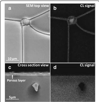
Because of the small crystallite size (in the range of 10–20 nm) that composes the porous layer, it is expected that such layer should emit radiation above the GaAs bandgap due to the quantum confinement effect [37]. In order to investigate this effect, we performed cathodoluminescence microanalysis of a GaAs sample before and after the porosification process. CL spectra from the reference sample show luminescence in the near infrared region with a maximum intensity at 860 nm as shown in Fig. 3. The peak is correlated to the interband recombination process of exited charge carriers across the direct bandgap of p-GaAs (1.43 eV) at room temperature [38]. After the porosification process, the CL intensity was considerably attenuated
and no detectable shift in the peak was observed despite the low crystallite size of the porous material. This indi-cates that no quantum confinement effect is created within the crystallites. Which is in contrast with the results obtained by Lockwood et al. who observed luminescence in the infrared (~840 nm) and green (~540 nm) PL peak wavelengths after anodic treatment in HCl solution that are consistent with an assignment to quantum confinement effects in GaAs micro- and nanocrystallites, respectively. The previous observations suggest that the size distribution of the pores correlated qualitatively with the intensities and the positions of the PL peaks, whereas variations in the chemical composition at the surface show no systematic correlation [39, 40]. The drastic decrease in the GaAs peak intensity could be due to different reasons, such as (i) the quenching of the CL due to the surface state, (ii) fractional amorphization of material during anodization, and (iii) change in chemical composition. The later assumption will be verified in the following paragraphs. However, less attention has been paid to the investigation of the direct correlation between luminescence properties and morphology features of the porous GaAs layer. The morphology and CL characteris-tics of porous layers reported on the spatial mapping of the intensity (Fig. 4) reveal luminescence only around the location of cracks formed during the porosification process. The cross-sectional CL maps also show no luminescence coming from the porous layer. These results suggest that the CL signal is coming from the underlying As2O3
Fig. 2 Planar-view SEM image of anodically etched p-GaAs layer formed in 49 % HF solution at 2 mA/cm2. Theinset shows high-resolution SEM image on the porous surface
400 500 600 700 800 900 0 500 1000 1500 2000
)
u-a(
yti
s
n
et
nI
Wavelenght (nm)
GaAs reference Porous layerFig. 3 Cathodoluminescence spectra at room temperature for the p-GaAs reference substrate and the porous p-GaAs with 20 keV at room temperature formed in 49 % HF solution at 2 mA/cm2
a
b
c
d
Fig. 4 SEM and CL micrographs taken from the top surface (a, b) and cross section (c, d) of porous p-GaAs with 20 keV at room temperature formed in 49 % HF solution at 2 mA/cm2
bulk GaAs material, which is exposed directly in the cracked areas or by the penetration of some electrons through porous layer at high accelerating voltage (20 KeV). The porous layer does not seem to generate detectable luminescence.
Chemical Compositions
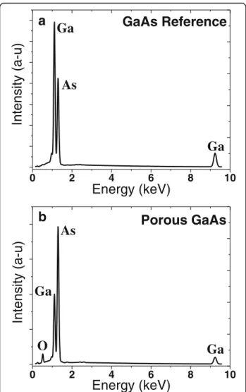
The absence of size-related luminescence could be due to non-radiative recombinations or to a drastic change in the chemical nature of porous material during anodi-zation. We have investigated this question by verifying that the porous material stoichiometry remained similar to that of GaAs after porosification. Figure 5 shows EDX spectra of the GaAs bulk reference sample and the por-ous GaAs sample. We notice that the ratio between the Ga- and As-related emissions is changed for the porous layer. It seems that the porous material is enriched with As relative to the reference sample and there is an
oxygen-related signal that appears as well. A similar EDX study shows a high decrease of Ga peak on crystal-line particles during the anodic dissolution of GaAs in HF solution [41, 42]. An oxygen peak is also present in the porous spectrum indicating a high concentration of oxygen in the film. The EDX mapping of the top of the porous sample confirms the presence of clusters with only As and O contents as shown in Fig. 6. Since the EDX spectrum integrates signals coming from the whole field of view, it is unclear if the oxygen is present in the porous material, or only in the clusters on the surface.
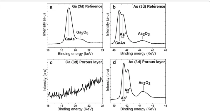
In order to determine the quantitative composition of the porous GaAs layer, we have performed XPS mea-surements before and after anodization. High-resolution spectra from the As 3d and Ga 3d regions are shown in Fig. 7. A small amount of Ga2O3and As2O3is detected on the surface of the reference sample (Fig. 7a, b) due to air exposure [34]. The Ga and As signals appear in the reference sample and are coming from both the base GaAs material as well as the oxides (Ga2O3and As2O3). The XPS analysis of the porous material (Fig. 7c, d) clearly shows that it consists only of As and arsenic
oxide elements. The Ga signal has completely
disappeared. However, the Ga presence in EDX spectra is due to the sensitivity of this technique that offers to probe the sample within few microns contrary to XPS measurement with depth analysis of about 8–10 nm. The elemental concentration of the porous layer taken at different surface locations is summarized in Table 1 and indicates that only As and O atoms are present in detectable quantities. This is due to the preferential dissolution of Ga during anodization, leaving a signifi-cantly higher As/Ga ratio in the porous layer. This is in agreement with the work of Steer et al. who have shown
0 2 4 6 8 10
O
Porous GaAs
)
u-a(
yti
s
n
et
nI
Energy (keV)
Ga
As
Ga
b
0 2 4 6 8 10Ga
As
)
u-a(
yti
s
n
et
nI
Energy (keV)
GaAs Reference
Ga
a
Fig. 5 EDX spectra of p-GaAs sample (a) and porous p-GaAs layer formed in 49 % HF solution at 2 mA/cm2(b)
10 µm As La Ga La O Ka
a
b
c
d
10 µm As La Ga La O Kaa
b
c
d
Fig. 6 EDX mapping of a porous p-GaAs layer formed in 49 % HF solution at 2 mA/cm2. a The top view SEM image and the EDX element maps for b As, c Ga, and d O elements
that Ga dissolved faster than arsenic during polarization in phosphoric acid [41].
Electrochemical Mechanisms
In order to explain the behavior of GaAs transformation to porous arsenic oxide under anodic bias, we propose a qualitative model based on the decomposition of com-pound semiconductors in contact with electrolytes [43]. Figure 8 schematically illustrates the etching mechanism of GaAs in a HF solution. The electrochemical dissolution of semiconductors depends essentially on the symmetry of bi-functional etching agents [44, 45]. The GaAs dissolution in HF is similar to InP in HCl [46]. The first step involves a synchronous exchange of bonds: Ga-F and As-H bonds replace the GaAs surface bonds [47]. The surface becomes H-passivated if the crystal was As-terminated or F-passivated if the crystal was Ga-terminated [48]. This reaction increases
the bond polarity of goshawks atoms. Since the surface atoms are doubly bonded to the bulk in the (001) orientations and triply bonded to the bulk in the (111) orientations [49], two and three GaAs bulk bonds must be broken to remove each atom from the lattice following:
GaAsþ 3HF→GaF3þ AsH3 ð1Þ
Note that the last GaAs bond should be broken without substitution to produce GaF3and AsH3.
The second step consists in the formation of arsenic. The elemental arsenic (As) can be obtained by two ways: (i) chemically: from the arsine molecules AsH3as shown in Fig. 8a. In this case, a non-uniform As layer was obtained due to the difficulty of the nucleation [34] following
2AsH3→2As þ 3H2 ð2Þ
(ii) Electrochemically: by involving holes (Fig. 8b) or protons (Fig. 8a) in a redox reaction following a three-hole mechanism proposed for the etching of GaP [50] and InP [46]. For p-GaAs, an accumulation of majority charge carriers (holes) takes place at the surface [51]. In aqueous HF solutions, three holes are required to dissolve one GaAs entity in which only the Ga element is oxidized. This highlights the increasing of the etch rate with the current density applied as shown in Fig. 1.
16 18 20 22 24
c
) u-a( yti s n et nIBinding energy (KeV) Ga (3d) Porous layer 16 18 20 22 24 ) u-a( yti s n et nI
Binding energy (keV)
Ga (3d) Reference
a
Ga2O3 GaAs 40 42 44 46 48 3/2 As0d
As2O3 As0 ) u-a( yti s n et nIBinding energy (KeV) As (3d) Porous layer 5/2 40 42 44 46 48 5/2
b
As2O3 ) u-a( yti s n et nIBinding energy (KeV) As (3d) Reference
GaAs As0
Fig. 7 Ga 3d and As 3d XPS spectra of p-GaAs reference (a, b) and porous p-GaAs samples (c, d) immediately after anodization in 49 % HF solution at 2 mA/cm2showing that only the As and O are present in detectable quantities
Table 1 Chemical composition of the porous sample by XPS measurements taken at the surface
Name Binding energy
(eV)
FWHM (eV)
% at conc % mass conc
O 1 s 531,2 2,605 23,46 6,15
Ga 3d 23,2 2,335 0,58 0,66
In this case, a uniform As layer was obtained due to the uniform injection of holes following
GaAsþ 3hþ→Ga3þþ As ð3Þ
It was observed that a brown film of As was formed on the electrode during electrochemical etching [34]. The same behavior was revealed in the case of InP etching in HCl solution with a high content of phosphorus but not indium [46]. We suggest that the injection of the holes anodically speeds up this selective etching which explains the low Ga concentration obtained previously in the porous layer.
The last step consists in the formation of As2O3. The presence of water in the electrolyte solution oxidizes elemental As following
Asþ 2H2Oþ 3hþ→AsO−2þ 4Hþ
2 AsO−2þ H2O→As2O3þ 2OH− ð4Þ Figure 8c shows 3D structures of As2O3 obtained on the electrode surface following reaction (2) or reaction (3) via As transformation to As2O3 by convective diffusion [52]. Additionally, the chemical formation of As2O3and the porosification process can take place sim-ultaneously, which produces a porous arsenic oxide layer as shown in Fig. 8d. The low crystallite dimension is
obtained by the nucleation and the coalescence of the oxide layer formed on the wall pores which will stop the reaction.
Structural Analyses
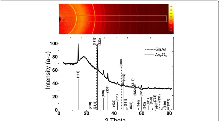
The last measurement was performed by powder XRD to investigate the crystal structure of the porous film. Figure 9 shows the diffractogram of a crushed porous layer obtained by scraping and grinding the porous sample to ensure that the measurement takes place on the porous layer and not on underlying GaAs substrate. The single-crystal X-ray diffraction measure-ment is obtained by mounting the crushed porous particles on the goniometer. All other diffraction peaks can be identified as the standard cubic of arsenolite structure (As2O3) with a lattice constant of 11.06 A°. No peak from other expected phases such as GaAs (zincblende) or As4O6 (cubic) are observed within the detection limit of our technique. Effectively, all the peaks correspond to the reflections from (111), (222), (400), and (331) planes of the cubic phase of As2O3 [53]. Hence, the XRD patterns show that the As2O3 film is of a single phase. The intensity of the (111) peak is very strong and its width at half maximum is relatively narrow, indicating a good crystallization state through a large crystallites size.
Conclusions
The nanostructural and chemical nature of porous layers obtained by the anodic etching of p-type GaAs has been investigated. No detectable CL has been attributed to the chemical change of porous GaAs during anodization. Chemical analysis shows that the porous material is depleted of Ga atoms and contains significant amounts of oxygen. Structural data from XRD show that the porous material is composed essentially of crystalline As2O3. An electrochemical process is proposed to explain such a behavior.
Abbreviations
CL:Cathodoluminescence; EDX: Energy-dispersive X-ray spectroscopy; XPS: X-ray photoelectron spectroscopy; XRD: X-ray diffraction
Acknowledgements
The authors would like to thank Sonia Blais and Stephane Gutierrez from the Centre de caractérisation des matériaux (CCM) for XPS and EDX characterizations and technical help, SUNLAB research group at the University of Ottawa for scientific discussions, the Natural Sciences and Engineering Research Council of Canada (NSERC), the Regroupement Quebecois sur les Matériaux de Pointe (RQMP), and the Fonds de Recherche du Quebec-Nature et Technologies (FRQNT) for financial support.
Funding
The study was funded by the Natural Sciences and Engineering Research Council of Canada (NSERC), the Regroupement Quebecois sur les Matériaux de Pointe (RQMP), and the Fonds de Recherche du Quebec-Nature et Technologies (FRQNT).
Authors’ contributions
YAB and AB conceived and designed the work. YAB prepared the samples and carried out the measurements. YAB and EP did the CL measurement. DD and RA supervised the research work. All authors read and approved the final manuscript.
Competing interests
The authors declare that they have no competing interests. Received: 27 April 2016 Accepted: 20 September 2016
References
1. Saxena D, Mokkapati S, Parkinson P, Jiang N, Gao Q, Tan H H, Jagadish (2013) Optically pumped room-temperature GaAs nanowire lasers. Nature Photonics 7: 963–968
2. Aberg I, Vescovi G, Asoli D, Naseem U, Gilboy JP, Sundvall C, Dahlgren A, Svensson KE, Anttu N, Bjork MT, Samuelson L (2016) A GaAs nanowire array solar cell with 15.3 % efficiency at 1 sun. IEEE J Photovoltaics 6:185–190 3. Tomioka K, Motohisa J, Hara S, Hiruma K, Fukui T (2010) GaAs/AlGaAs core
multishell nanowire-based light-emitting diodes on Si. Nano Lett 10:1639–1644 4. Ganjipour B, Wallentin J, Borgstrom MT, Samuelson L, Thelander C (2012)
Tunnel field-effect transistors based on InP-GaAs heterostructure nanowires. ACS Nano 6:3109–3113
5. Martin PN, Aksamija Z, Pop E, Ravaioli U (2010) Reduced thermal conductivity in nanoengineered rough Ge and GaAs nanowires. Nano Lett 10:1120–1124 6. Nazemi E, Aithal S, Hassen WM, Frost EH, Dubowski JJ (2015) GaAs/AlGaAs
heterostructure based photonic biosensor for rapid detection of Escherichia coli in phosphate buffered saline solution. Sensors Actuators B Chem 207:556–562
7. Braive R, Le Gratiet L, Guilet S, Patriarche G, Lemaı̂tre A, Beveratos A, Robert-Philip I, Sagnes I (2009) Inductively coupled plasma etching of GaAs suspended photonic crystal cavities. J Vac Sci Technol B 27:1909–1914 8. Lee JH, Wang ZM, Abuwaar ZY, Salamo GJ (2009) Design of nanostructure
complexes by droplet epitaxy. Cryst Growth Des 9:715–721
0 20 40 60 80 0 20 40 60 80 100
)
u-a(
yti
s
n
et
nI
2 Theta
(331) (40 0 ) (311) (200) (111) (911) (840) (644) (73 3 ) (731) (642) (551) (444) (622) (533) (531) (44 0) (511) (422) (331) (400) (222) (311) (220) (11 1) ---GaAs As2O3Fig. 9 Powder XRD of porous p-GaAs layer formed in 49 % HF solution at 2 mA/cm2which corresponds to As 2O3crystal
9. Dejarld MT, Shin JC, Chern W, Chanda D, Balasundaram K, Rogers JA, Li X (2011) Formation of high aspect ratio GaAs nanostructures with metal assisted chemical etching. Nano Lett 11:49–54
10. Ritenour AJ, Levinrad S, Bradley C, Cramer RC, Boettcher SW (2013) Electrochemical nanostructuring of n-GaAs photoelectrodes. ACS Nano 7:6840–6849
11. Dimastrodonato V, Mereni LO, Young RJ, Pelucchi E (2010) AlGaAs/GaAs/AlGaAs quantum wells as a sensitive tool for the MOVPE reactor environment. J Cryst Growth 312:3057–3062
12. Ermez S, Jones EJ, Crawford SC, Gradečak S (2015) Self-seeded growth of GaAs nanowires by metal–organic chemical vapor deposition. Cryst Growth Des 15:2768–2774
13. Heyn C, Stemmann A, Klingbeil M, Strelow C, Koppen T, Mendach S, Hansen W (2011) Mechanism and applications of local droplet etching. J Cryst Growth 323:263–266
14. Lee JH, Wang ZM, Strom NW, Mazur YI, Salamo GJ (2006) InGaAs quantum dot molecules around self-assembled GaAs nanomound templates. Appl Phys Lett 89:202101
15. Mano T, Kuroda T, Sanguinetti S, Ochiai T, Tateno T, Kim J, Noda T, Kawabe M, Sakoda K, Kido G, Koguchi N (2005) Self-assembly of concentric quantum double rings. Nano Lett 5:425–42
16. Kaizu T, Tamura Y, Igarashi M, Hu W, Tsukamoto R, Yamashita I, Samukawa S, Okada Y (2012) Photoluminescence from GaAs nanodisks fabricated by using combination of neutral beam etching and atomic hydrogen-assisted molecular beam epitaxy regrowth. Appl Phys Lett 101:113108
17. Somaschini C, Bietti S, Sanguinetti S, Koguchi N, Fedorov A (2010) Self-assembled GaAs/AlGaAs coupled quantum ring-disk structures by droplet epitaxy. Nanotechnology 21:125601
18. Mariani G, Wong PS, Katzenmeyer AM, Léonard F, Shapiro J, Huffaker DL (2011) Patterned radial GaAs nanopillar solar cells. Nano Lett 11:2490–2494 19. Stemmann A, Heyn C, Köppen T, Kipp T, Hansen W (2008) Local droplet
etching of nanoholes and rings on GaAs and AlGaAs surfaces. Appl Phys Lett 93:123108
20. Föll H, Carstensen J, Langa S, Christophersen M, Tiginyanu IM (2003) Porous III–V compound semiconductors: formation, properties, and comparison to silicon. Phys Status Solidi 197:61–70
21. Flamand G, Poortmans J (2005) Porous GaAs as a possible antireflective coating and optical diffusor for III-V solar cells. Phys Status Solidi (a) 202:1611–1615 22. Dimitrakopulos GP, Bazioti C, Grym J, Gladkov P, Hulicius E, Pangrác J,
Pacherová O, Komninou P (2014) Misfit dislocation reduction in InGaAs epilayers grown on porous GaAs substrates. Appl Surf Sci 306:89–93 23. Rojas EG, Terheiden B, Plagwitz H, Hampe C, Tutuc D, Haug R, Brendel R
(2009) Mesoporous GaAs double layers for layer transfer processes. Phys Status Solidi A 206:2872–2875
24. Boucherif A, Beaudin G, Aimez V, Arès R (2013) Mesoporous germanium morphology transformation for lift-off process and substrate re-use. Appl Phys Lett 102:011915
25. Salehi A, Kalantari DJ, Goshtasbi A (2006) Rapid response of Au/porous-GaAs humidity sensor at room temperature. Conf Optoelectron Microelectron Mater Devices 79:125–128
26. Grym J, Nohavica D, Gladkov P, Hulicius E, Pangrác J, Piksová K (2013) Epitaxial growth on porous GaAs substrates. Comptes Rendus Chim 16:59–64 27. Li X, Guo Z, Xiao Y, Um HD, Lee JH (2011) Electrochemically etched
pores and wires on smooth and textured GaAs surfaces. Electrochim Acta 56:5071–5079
28. Tiginyanu I, Langa S, Foell H, Ursachi V (2009) Porous III-V semiconductors, online book: http://www.porous-35.com
29. Rojas EG (2009) Formation of mesoporous germanium by electrochemical etching for lift-off processes. 24th IEEE Eur. Photovolt. Sol. Energy Conf. Exhib. Hamburg, Germany. doi:10.1109/PVSC.2009.5411208
30. Blaffart F, Boucherif A, Aimez V, Arès R (2013) Control of mesoporous silicon initiation by cathodic passivation. Electrochem Commun 36:84–87 31. Bioud YA, Boucherif A, Fafard S, Aimez V, Drouin D, Ares R (2015) Systematic
study of mesoporous germanium formation regimes by bipolar electrochemical etching. 9th Int. Conf. Silicon Ep. Heterostruct, Montreal, Canada
32. Bellet D, Canham LT (1997) Drying of porous silicon, in properties of porous silicon. Inst Eng Technol 5:932
33. Kowalski SJ, Banaszak J (2013) Modeling and experimental identification of cracks in porous materials during drying. Dry Technol 31:1388–1399
34. Smeenk NJ, Engel J, Mulder P, Bauhuis GJ, Bissels GMMW, Schermer JJ, Vlieg E, Kelly JJ (2012) Arsenic formation on GaAs during etching in HF solutions: relevance for the epitaxial lift-off process. ECS J Solid State Sci Technol 2:58–65 35. Ballirano P, Maras A (2002) Refinement of the crystal structure of arsenolite,
As2O3. NCS 217:177–178
36. Anthony JW Arsenolite As2O3(2005) In Handbook of Mineralogy. Mineral Data Publishing. p 23–24
37. Kuroda T, Mano T, Ochiai T, Sanguinetti S, Sakoda K, Kido G, Koguchi N (2005) Optical transitions in quantum ring complexes. Phys Rev B 72:1–8 38. Kittel C (1986) Introduction to solid state physics. Wiley India Pvt. p 139–140 39. Lockwood DJ, Schmuki P, Labbé HJ, Fraser JW (1999) Optical properties of
porous GaAs. Physica E 4:102–110
40. Schmuki P, Lockwood DJ, Labbé HJ, Fraser JW (1996) Visible photoluminescence from porous GaAs. Appl Phys Lett 69:1620
41. Steer CA, Weng GS, Luo JL, Ivey DG (2000) Formation of As2O3during anodic dissolution of GaAs. Electrochem Commun 2:754–761
42. Bioud YA, Boucherif A, Belarouci A, Paradis E, Drouin D, Ares R (2016) Chemical composition of anodically formed p-type porous GaAs in HF based electrolyte. 10th Int. Conf. Porous Semiconductors - Science and Technology, Tarragona, Spain
43. Gerische H (1978) Electrolytic decomposition and photodecomposition of compound semiconductors in contact with electrolytes. J Vac Sci Technol 15:1422–1428
44. Mint W, Gerischer H (1968) The mechanisms of the decomposition of semiconductors by electrochemical oxidation and reduction. Electrochim Acta 13:1329–1341
45. Wallem-Mattes I, Gerischer H (1969) The Mechanism of the resolution of gallium arsenide by oxidants. Z Phys Chem 64:187–198
46. Notten PHL (1984) The etching of InP in HCl solutions: a chemical mechanism. J Electrochem Soc 131:2641
47. Wang W, Lee G, Huang M, Wallace RM, Cho K (2010) First-principles study of GaAs(001)-β2 (2×4) surface oxidation and passivation with H, Cl, S, F, and GaO. J Appl Phys 107:103720
48. Adachi S, Kikuchi D (2000) Chemical etching characteristics of GaAs(100) surfaces in aqueous HF solutions. J Electrochem Soc 147:4618–4624 49. Ross FM, Oskam G, Searson PC, Macaulay JM, Liddle JA (1997)
Crystallographic aspects of pore formation in gallium arsenide and silicon. Philos Mag A 75:525–539
50. Schwandt G, Memming R (1968) Electrochemical properties of gallium phosphide in aqueous solutions. Electrochim Acta 13:1299–1310 51. Schmuki P, Fraser J, Vitus CM, Graham MJ, Isaacs HS (1996) Initiation and
formation of porous GaAs. J Electrochem Soc 143:3316–3322
52 Dai Q, Hu J, Salmeron M (1997) Adsorption of water on NaCl (100) surfaces: role of atomic steps. J Phys Chem B 101:1994–1998
53 Bozorth RM (1923) The crystal structures of the cubic forms of arsenious and antimonous oxides. J Am Chem Soc 45:1624–1627
Submit your manuscript to a
journal and benefi t from:
7 Convenient online submission 7 Rigorous peer review7 Immediate publication on acceptance 7 Open access: articles freely available online 7 High visibility within the fi eld
7 Retaining the copyright to your article