Arrays of holes fabricated by electron-beam lithography combined with image reversal
process using nickel pulse reversal plating
Yousef Awad, Eric Lavallée, Kien Mun Lau, Jacques Beauvais, Dominique Drouin, Melanie Cloutier, David Turcotte, Pan Yang, and Prasad Kelkar
Citation: Journal of Vacuum Science & Technology A: Vacuum, Surfaces, and Films 22, 1040 (2004); doi: 10.1116/1.1647589
View online: http://dx.doi.org/10.1116/1.1647589
View Table of Contents: http://avs.scitation.org/toc/jva/22/3
I. INTRODUCTION
Hole arrays fabricated in GaAs have been used in appli-cation for photonic bandgap waveguides.1 Ebbesen et al.2 showed that hole arrays can be used for extraordinary optical transmission through sub-wavelength holes. Periodic struc-ture of holes can also be used for the purpose of designing new guiding microwave structures.3The reversal imprinting method has been used recently as an alternative to conven-tional nanoimprint lithography.4 This method offers an ad-vantage over conventional nanoimprinting by allowing im-printing onto substrates that cannot be easily spin coated, such as flexible polymer substrates. Nanoindentation using scanning probe microscope5has been used to fabricate arrays of high-aspect-ratio holes. Fernandez et al.6 studied the use of interference lithography for large-scale production of holes array. This approach, however, suffers from hard-to-achieve exposure repeatability, besides maintaining good uniformity of the patterns, which requires perfectly aligned beams. Other researchers7modified the shape of the incident intensity distribution to fabricate arrays of holes, by interfer-ing more than two beams. Although many different configu-rations of multiple beams can increase image contrast, only those that satisfy certain symmetry requirements preserve the large depth of field characteristic of two beams. To make fine hole patterns, application of optical lithographic techniques such as utilizing an attenuating phase shift mask is used to enhance the resolution,8 however, the diameter formed by this approach is restricted to 0.20m using the KrF excimer laser. Nakao et al.9 have used phase shift masks using KrF excimer laser as exposure light to fabricate 0.1 m dense holes.
In this article, a simple fabrication method for a nano-imprint lithography mold is demonstrated. This method con-sists of four major processing steps: stack deposition, e-beam lithography, image reversal, and etching. As it was demon-strated by Alkaisi et al.,10 silicon nitride as a mold material for nanoimprint lithography presents several advantages
in-cluding nonsticking problems between the mold and the used polymer, which may eliminate the need for a release agent or surfactant to overcome the sticking problems. Furthermore, performing the nanoimprint lithography at low temperatures and low pressure could be easily achieved using silicon ni-tride as a mold material. In this article, sub-100 nm pattern-ing is performed uspattern-ing a negative dry e-beam resist. Dry resist is a desirable alternative to wet resist, because pinhole free, good adhesion, uniform and ultrathin film deposition can be achieved easily. Furthermore, dry resists can be de-posited on a three-dimensional surface,11or on a very small surface like on tip of monomode fiber.12,13The processing of dry resists has attracted considerable attention in recent years. Many researchers used plasma deposition14,15 sublima-tion or thermal evaporasublima-tion12to apply dry e-beam resist on a substrate.
To obtain an array of holes, image reversal is performed by plating a thin Ni layer around the exposed resist struc-tures, converting the resist structure into an opening suitable for conventional reactive ion etching. The final step was to use conventional reactive ion etching to ash the resist and to etch through the opening into the underlying layers.
II. EXPERIMENT
Figure 1 shows the hole array fabrication process flow used in this work. The fabrication of an array of nanoscale high-aspect-ratio holes consists of four major steps: substrate preparation, patterning, electroplating, and conventional re-active ion etching共RIE兲.
In stack preparation, a 300 nm thick Si3N4was deposited by LPCVD on a 365 m thick 关100兴 Si substrate. The LPCVD Si3N4 layer is deposited under light tensile stress, which is believed to reduce the mechanical strain on the nano-scale pillars on the final mold. A thin 共20 nm兲 silver plating seed layer is deposited on the silicon nitride coated wafer by electron gun evaporation. Silver was chosen as the seed layer for its excellent electrical conductivity and it can be easily dry etched using the same dry etch gas mixture that is being used to etch the underlying Si3N4 layer. A 30 nm a兲Electronic mail: [email protected]
thick layer of QSR-5,16 a negative dry electron-beam resist which consists mainly of nonpolymeric sterol molecules, is then evaporated on top of the seed layer.
In patterning the substrate, an array of dots was formed in the negative resist by using electron-beam lithography. Pat-terning the resist was performed using a LEO 1530 field emission gun scanning electron microscope 共FEG-SEM兲 ex-ternally controlled by the Nabity Pattern Generation System 9.0. The electron source for this system is a field emission gun 共FEG兲 which makes it possible to maintain a beam di-ameter better than 5 nm even at low energy 共⬍15 keV兲 and at a beam current of 900 pA. The patterning was done at 10 keV energy. In order to reduce the processing time for the pattern containing arrays of dots, a single point exposure scheme was used for each point. This was performed by stepping the beam by 270 nm increments to fill large squares fields 共200⫻200兲 m2. The overall exposure dose in the fields is 700 C/cm2, which yields to a point dose of 0.5 pC/point. After exposure, development of the resist was car-ried out by immersion in a methyl ethyl ketone共MEK兲 bath for 10 s, followed by water rinse and then dried using N2.
An image reversal process using Ni pulse reversal plating was used to reverse the tonality of the pattern and to form a hard-etch mask for RIE. Ni electrodeposition was carried out using a commercial plating solution of nickel sulfamate salt without organic additives. Pulse reversal technique was used in this study to improve via/trench filling capability, and to enhance the dissolution of unwanted grains. For the plating of a 20–30 nm nickel film, precise control of the elec-trodeposition is critical, since the plating rate from the com-mercial nickel sulfamate bath used in previous works17–19 was ⬃10 nm/s, using such a plating rate makes the
deposi-tion of 20–30 nm thin film extremely hard to achieve. Fur-thermore, grain refinement, porosity improvement, and mini-mization of overplating are essential issues when plating around a resist structure with a 30 nm thickness.
The plating parameters: average current density, duty cycle, plating frequency, bath temperature, and agitation, were studied and optimized to produce extremely fine-grained共i.e., nanocrystalline兲 deposits free from voids or de-fects at a very slow plating rate as discussed in the following section. The plated thin film has to be free from voids or defects in order to protect the underlaying substrate during dry etching. It is important to note that stripping the resist patterns, dry etching of Ag film and subsequently the Si3N4 layer were carried out in one etching step in a March 1701 RIE system using a SF6:CH4 mixture at a power of 100 W for 30 min. After eching through the holes, the Ni etch mask as well as the silver seed layer were stripped off using con-centrated nitric acid.
III. RESULTS AND DISCUSSION
Combining e-beam lithography with image reversal and conventional reactive ion etching offers the prospect of pat-terning arrays of holes with the desired aspect ratio.
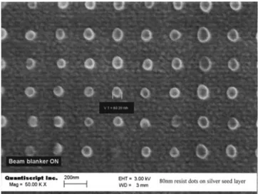
Figure 2 shows a SEM of an average 80 nm diam, 30 nm height dots fabricated in the negative resist. The smoothest surface and the smallest grain size have been achieved by combining a current reversal plating at 400 kHz frequency, 80% duty cycle, ultrasonic bath having a power of 80 W, bath temperature of 45 °C, and 1.5 mA/cm2 average current density. A plating rate as low as 0.2 nm/s is obtained using these conditions. This yields a deposit with a mirror smooth finish without any visible grains or holes. Since the plating rate is extremely low, very accurate control of the film thick-ness is obtained. Figure 3 shows a scanning electron micros-copy共SEM兲 of high resolution image of arrays of holes sur-FIG. 1. Process steps for the fabrication of hole arrays.
FIG. 2. Array of 100 nm diam dots patterned in 30 nm thick dry resist
共QSR-5兲.
1041 Awadet al.: Arrays of holes fabricated by electron beam 1041
rounded by 25 nm thick plated Ni that has been used as a hard etch mask for these holes. As it can be seen from Fig. 3 the Ni surface is smooth free from voids with little defects and certainly conformed precisely to the e-beam written re-sist structures. The average size and pitch of the holes were 100 and 270 nm, respectively. The test pattern holes, after etching through the Si3N4 substrate, have an average diam-eter of 100 nm with 3⫽21 nm. Figure 4 shows a SEM high resolution image of holes etched in the Si3N4 underlayer after stripping of the plated Ni and the Ag seed layer. It is important to mention that the holes have the same size after stripping the Ni and Ag. This experiment confirmed the ex-cellent performance of the electroplated nickel as a hard-etch mask. The superior etching resistance of Ni, in addition to its mirrorlike surface and the ability to plate very thin films, makes this technique very suitable to be employed for those applications that are demanding in terms of accuracy and etch depth. It is important to note that no dose correction or
In conclusion, holes array of 100 nm diam 270 nm pitch has been fabricated using a dry e-beam resist, e-beam lithog-raphy, electroplating, and conventional RIE. It has been es-tablished in the present work that a nickel film of 25 nm thickness free from voids or defects is deposited using pulse reversal plating. It should also be pointed out that a plating rate as low as 0.2 nm/s is achieved in this work which in turn makes very accurate control of the deposit thickness an easy task to achieve by accurate control of the plating parameters. The process can be applied to invert any pattern on any sur-face since it does not require any spin coating. More work is in process to enhance the resolution limit of the dry resist that is being used in this study. Nevertheless, the current results demonstrate the compatibility of this fabrication method with large arrays of holes for optoelectronic and mi-croelectronics applications.
1M. Nakao, S. Oku, H. Tanaka, Y. Shibata, A. Yokoo, T. Tamamura, and H.
Masuda, Opt. Quantum Electron. 34, 183共2002兲.
2T. Ebbesen, H. Lezec, H. Ghaemi, T. Thio, and P. Wolff, Nature共London兲
391, 667共1998兲.
3A. Zeid and H. Baudrand, IEEE Trans. Microwave Theory Tech. 50, 1198 共2002兲.
4
X. D. Huang, L.-R. Bao, X. Cheng, L. J. Guo, S. W. Pang, and A. F. Yee, J. Vac. Sci. Technol. B 20, 2872共2002兲.
5H. Masuda, K. Kanezawa, and K. Nishio, Chem. Lett. 31, 1218 共2002兲.
6
A. Fernandez, J. Y. Decker, S. M. Herman, D. W. Phillion, D. W. Sweeney, and M. D. Perry, J. Vac. Sci. Technol. B 15, 2439共1997兲.
7X. Chen, S. H. Zaidi, S. R. J. Brueck, and D. J. Devine, J. Vac. Sci.
Technol. B 14, 3339共1996兲.
8
T. Terasawa, N. Hasegawa, H. Fukuda, and S. Katagiri, Jpn. J. Appl. Phys., Part 1 30, 2991共1991兲.
9S. Nakao, A. Nakae, A. Yamaguchi, K. Tsujita, and W. Wakamiya, Jpn. J.
Appl. Phys., Part 1 38, 2686共1999兲.
10M. M. Alkaisi, R. J. Blaikie, and S. J. McNab, Microelectron. Eng. 57-58,
367共2001兲.
11S. Babin and H. W. P. Koops, J. Vac. Sci. Technol. B 14, 3860共1996兲. 12V. Foglietti, E. Cianci, and G. Giannini, Microelectron. Eng. 57-58, 807
共2001兲. 13
S. Babin, M. Weber, and H. W. P. Koops, J. Vac. Sci. Technol. B 14, 4076
共1996兲.
14S. Morita et al., J. Appl. Phys. 51, 3938共1980兲.
15F. O. Fong, H. C. Kuo, J. C. Wolfe, and J. N. Randall, J. Vac. Sci.
Technol. B 6, 357共1988兲.
16
E. Lavalle´e, J. Beauvais, D. Drouin, and M. Cloutier, U.S. patent pending. FIG. 3. SEM of 25 nm thick plated Ni around arrays of dots in the resist.
FIG. 4. Array of 110 nm holes after dry etch of Ag seed layer and the subsequent Si3N4layer, followed by removal or the etch mask and the seed
17J. Spector, C. J. Jacobsen, and D. M. Tennant, J. Vac. Sci. Technol. B 15,
2872共1997兲.
18D. Weiss, M. Peuker, and G. Schneider, Appl. Phys. Lett. 72, 1805 共1998兲.
19G. Schneider, T. Schliebe, and H. Aschoff, J. Vac. Sci. Technol. B 13,
2809共1995兲.
20
Y. Awad, E. Lavallee, J. Beauvais, D. Drouin, Pan Yang, D. Turcotte, and Lau Kien Mun, J. Vac. Sci. Technol. B 20, 3040共2002兲.
21L.-R. Bao, X. D. Huang, L. J. Guo, S. W. Pang, and A. F. Yee, J. Vac. Sci.
Technol. B 20, 2881共2002兲.
1043 Awadet al.: Arrays of holes fabricated by electron beam 1043