Electrical modelling of interface traps in GeSn MOS structures
B. Baerta, D. Cerica, M. Schmeits and N. D. Nguyen
Solid State Physics – Interfaces and nanostructures, University of Liege, B-4000 Liege, Belgium
Introduction
On the road towards next-generation high-mobility channel CMOS and optoelectronic devices, new materials are being investigated. The semiconducting alloy germanium tin (GeSn) is seen as a good candidate because of two interesting properties: a direct bandgap for Sn concentrations starting around 10% and the increase of the hole and electron mobilities by inducing strain due to the lattice mismatch with Ge and Si [1,2]. The recent development of GeSn-based MOSFETs [3–5] requires the assessment of defect states at the interface between the oxide and the semiconductor. Techniques that have been used successfully with silicon, such as the conductance method, cannot be applied directly to structures made out of these new materials without particular care. Martens et al. [6] have shown that in low bandgap materials such as Ge, the interface trap density can be easily under- or overestimated. As the bandgap of GeSn materials is even smaller than that of Ge, we expect to encounter the same or even higher difficulties when applying the technique on GeSn MOS structures.
Method
Our approach is based on a numerical simulation software that we specifically designed in the objective of modeling the electrical properties of semiconducting structures by solving the basic semiconductor equations. Using a finite-difference method and a Scharfetter-Gummel discretization scheme [7], we obtained, as results of the simulations, impedance (admittance) characteristics for various sets of physical parameters such as dopant concentrations and interface traps density (Fig. 1). We have therefore performed a systematic study of the energy distribution of interface states in GeSn MOS structures. The key elements in the theoretical electrical signatures of interface traps in such structures under ac regime have been studied, in view of clarifying in a comprehensive way the role of interface traps in electrical characteristics such as CV and impedance spectroscopy, which are dominantly used by all device makers. The structure used in our study is made out of a metal contact deposited on a 9 nm thick oxide layer on top of a 100 nm p-type doped GeSn layer.
Results
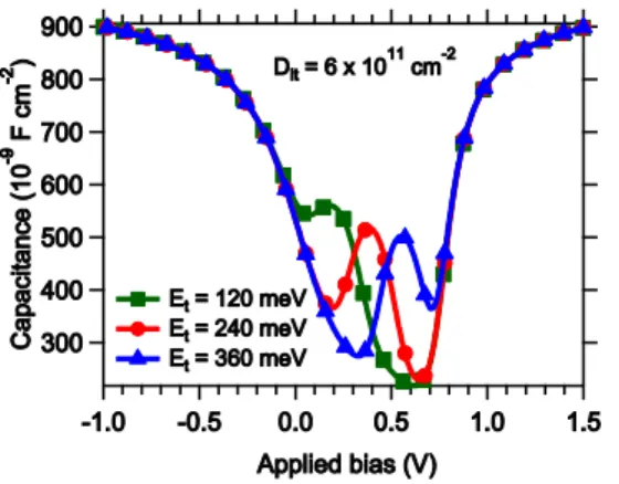
The numerical analysis enabled us to highlight the direct relationship between properties of the interface trap density and the features observed in the C–V characteristics and conductance resulting from the simulations. Notably, we observed that the conductance response peak and position at low inversion varies with the interface trap density and energy position (Fig. 2). We then show that the shift of the Fermi level with the applied bias is also dependent on those two parameters. We subsequently noticed that the interface trap density can be determined for trap energies closer to mid-gap. However, the analysis of the conductance response is more challenging when the trap energy is closer to the band edges.
Similar results have been obtained for traps extending over a wider energy range within the bandgap and the influence of other parameters such as the carrier mobilities, capture cross-sections and temperature is investigated. It is also emphasized that our simulation software allowed us to gain even more insight into the influences of the various parameters which come into play when confronted with experimental data, thanks to the ability to access many microscopic properties such as Fermi level, position-dependent carrier concentration and trap occupancy. Using this numerical tool and these theoretical results, the interpretation of experimental measurements on similar GeSn based MOS structures would therefore be facilitated.
Acknowledgements
The authors gratefully acknowledge discussions and suggestions from E. Simoen (imec).
References
[1] B. Vincent, Y. Shimura, S. Takeuchi, T. Nishimura, G. Eneman et al., Microelectron. Eng. 88 (4) (2011) p. 342 [2] R. Roucka, J. Tolle, C. Cook, A. Chizmeshya, J. Kouvetakis et al., Appl. Phys. Lett. 86 (19) (2005), 191912. [3] L. Wang, S. Su, W. Wang, X. Gong, Y. Yang, P. Guo, G. Zhang et al., Solid-State Electron 83 (2013) p. 66 [4] S. Gupta, R. Chen, B. Vincent, D. Lin, B. Magyari-Kope, M. Caymax et al., ECS Trans. 50 (9) (2013) p. 937 [5] S. Wirths, A.T. Tiedemann, Z. Ikonic, P. Harrison et al., Appl. Phys. Lett. 102 (19) (2013) 192103,
[6] K. Martens, C. Chui, G. Brammertz, B. De Jaeger et al., IEEE Trans. Electron Devices 55 (2) (2008) p. 547 [7] B. Baert, M. Schmeits and N.D. Nguyen, Appl. Surf. Sci. 291 (2014), p. 25
Figure 1: Schematic of the position of the interface states within the bandgap, with energies from 180 meV to 420 meV above the valence band energy.
Figure 2: Low frequency (1 kHz) C–V characteristics for different interface traps energy positions Et relative to the
valence band energy and an interface trap density of 6 × 1011 cm−2.
Figure 3: (Gp /ω)max (as a function of frequency) plotted as a function of Fermi level at the interface for trap energies
extending over a range of 120 meV, different positions in the bandgap and different trap densities (6 × 1011 cm−2 – lower curves – and 1.2 × 1012 cm−2 – upper curves).