Temperatureeffect Ofelectricalproperties Of Cigs Solar
8
0
0
Texte intégral
(2) A. K. Ferouani et al.. J Fundam Appl Sci. 2011, 3(1), 77-84. 78. A CIGS solar cell is built up of a substrate of soda-lime glass, a back contact of molybdenum (Mo), a light absorbing layer consisting of copper indium gallium diselenide (Cu(In;Ga)Se2), a buffer layer of cadmium sulphide (CdS) or zinc oxy sulphide (Zn(O; S)), a thin layer of high resistive zinc oxide (ZnO) and a transparent front contact of aluminium doped zinc oxide (ZnO:Al). Figure 1 shows the cross section of a CIGS solar cell with typical thicknesses of the different layers indicated.. Fig.1. A schematic of a typical CIGS solar cell. 2. SOLAR CELL OUTPUT PARAMETERS J-V measurements are performed to characterize solar cells. Figure 4 shows a typical JV curve with some of the following solar cell output parameters indicated [2]: *Short-circuit current, Jsc, is the maximum current at zero voltage. The short-circuit current density, Jsc, *Open-circuit voltage, Voc, is the maximum voltage at zero current. *Maximum power point, Pmp, is the maximum power output at optimal operating condition,i.e. Pmp = Vmp Jmp. *Fill factor, FF, is a measure of how square the J-V curve is. It is defined As. FF . J mpV mp J scVco. . p mp Voc J sc. (1).. *Efficiency, , is the energy-conversion efficiency. It is given by (1).
(3) A. K. Ferouani et al.. J Fundam Appl Sci. 2011, 3(1), 77-84. . Pmp Pin. . J scVoc Pin. 79. (2).. where Pin is the total power of the incident light.. QE measurements are another method for characterization of solar cells: *Quantum efficiency, QE, is the number of generated electron-hole pairs per incident photon in the solar cell. When measured with an external circuit this quantity is also referred to as the external quantum efficiency, EQE. It is often measured for wavelengths, , in the range from 200nm to 1200nm.The short-circuit current density can be calculated from the measurement As. . . J sc EQE ( )( )d. (3).. 0. Where is the photon flux at the AM 1:5 spectrum The model of a CIGS solar cell module has to take into account electrical, optical and geometrical parameters [3]. The CIGS layer provides a shunting path between the front contact and the back contact, indicated in Figure 2.. Fig.2. Equivalent electrical circuit of a CIGS solar cell. The one-diode model, shunt resistances and series resistances are shown. Voltages, currents and dimensions are defined. After Ref. [4] and [3]..
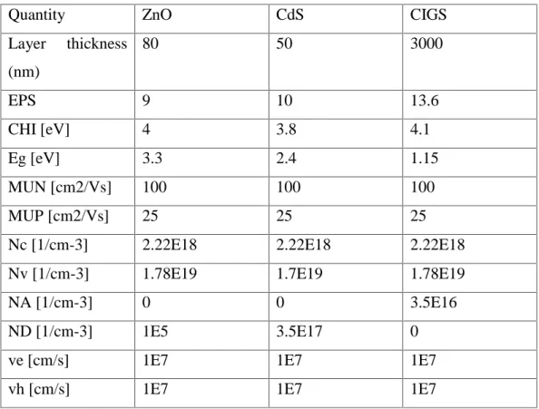
(4) A. K. Ferouani et al.. J Fundam Appl Sci. 2011, 3(1), 77-84. 80. 3. SIMULATIONS, RESULTS AND DISCUSSIONS Solar cells. It is developed especially for CdTe and CIGS solar cells.SCAPS is used to replicate and investigate all the available research-level CIGS solar cells with various buffer layers. From the solution provided by an SCAPS [5] simulation, output such as current voltage characteristics in the dark and under illumination can be obtained. These may be computed as a function of temperature. For solar cell and detector structures, collection efficiencies as a function of voltage, light bias, and temperature can also be obtained. By incorporating the various material parameters into SCAPS for all of the analysis aspects, changes in the values for efficiency, Voc, Jsc and FF as well as the effect of operating temperature are observed. Tables 1 and 2 shows the description of the parameters in the simulation and the base parameters that have been used in this study [5]. SCAPS is a one dimensional computer software to simulate the AC and DC electrical characteristics of thin film.. Table 1. Overall electronic properties. EPS Relative permittivity, er MDN Electron band mobility, ln (cm2/V s) MDP Hole band mobility, lp (cm2/V s) NA Acceptor concentration (1/cm3) ND Donor concentration (1/cm3) EG Electrical band gap (eV) NC Effective density of states in conduction band (1/cm3) NV Effective density of states in valence band (1/cm3) CHI Electron affinity, xe (eV).
(5) A. K. Ferouani et al.. J Fundam Appl Sci. 2011, 3(1), 77-84. 81. Table 2. Base parameters for ZnO/CdS/CIGS. Quantity Layer. ZnO thickness 80. CdS. CIGS. 50. 3000. (nm) EPS. 9. 10. 13.6. CHI [eV]. 4. 3.8. 4.1. Eg [eV]. 3.3. 2.4. 1.15. MUN [cm2/Vs]. 100. 100. 100. MUP [cm2/Vs]. 25. 25. 25. Nc [1/cm-3]. 2.22E18. 2.22E18. 2.22E18. Nv [1/cm-3]. 1.78E19. 1.7E19. 1.78E19. NA [1/cm-3]. 0. 0. 3.5E16. ND [1/cm-3]. 1E5. 3.5E17. 0. ve [cm/s]. 1E7. 1E7. 1E7. vh [cm/s]. 1E7. 1E7. 1E7. The obtained results in figure.3 demonstrate an optimum current density at very low bias and an optimum power at 0.5 volt at 300 K temperature. We have remarked also in figure.4 a more stability of current-density curves for temperatures less then 320K and an instability of the curves for temperatures >340K. As soon as power is more optimum with low temperatures (<320K). From figures 5. A,B,C and D the Voc is more optimized at 300K, the Jsc is stable at the range of temperatures 300-400K, the FF is optimized for <350K and minimized for temperatures > 360K and finally the effiency of our solar cells is optimized for a temperature of work of 300K..
(6) A. K. Ferouani et al.. J Fundam Appl Sci. 2011, 3(1), 77-84. 0.05. 2. Power(W/cm ). 2. Current density(mA/cm ). 0.04. 0.03. 0.02. 0.01. J-V curve P-V curve. 0.00 0.0. 0.1. 0.2. 0.3. 0.4. 0.5. 0.6. Voltage (V). Fig.3. J–V and the power characteristics of CIGS solar cell at 300K. 2. Current density(mA/cm). 0.155. 0.150. 0.145. (300 K) (320 k) (340 k) (360 k) (380 k) (400 k). 0.140. 0.135. 0.130. 0.125 -0.1. 0.0. 0.1. 0.2. 0.3. 0.4. 0.5. 0.6. 0.7. 0.8. Voltage (V). Fig.4. J–V characteristics of solar cell with variable the temperature of CIGS. 82.
(7) A. K. Ferouani et al.. J Fundam Appl Sci. 2011, 3(1), 77-84. (A). 83. (B). 44. 600 42 40 2. JSC(mA/Cm ). Voc(mV). 500. 400. 38 36 34. 300 32. 200. 30. 300. 320. 340. 360. 380. 400. 300. 320. 340. 360. 380. 400. TEMPERATURE (K). TEMPERATURE (K). (C). (D) 21 20 70. 19. EFFIENCY %. 60. FF (%). 50 40 30 20. 18 17 16 15 14. 10. 13. 0 300. 320. 340. 360. TEMPERATURE (K). 380. 400. 12 300. 320. 340. 360. 380. TEMPERATURE (K). Fig.5. Solar cell performance of the CIGS cells with different buffer layers.. 4. CONCLUSION Various temperature for a possible study of electrical parameters of CIGS solar cells have been investigated in terms overall cell performance at thickness of CIGS layer. For. 400.
(8) A. K. Ferouani et al.. J Fundam Appl Sci. 2011, 3(1), 77-84. 84. an optimum thickness of around 3 µm of high-efficiency CIGS absorber, the optimum thickness of buffer layers is found to be 50 nm. Simulation results show that the solar cell performances are affected by the increase in operating temperature for all CIGS semiconductor with differences in the temperature gradients. The gradient of temperature has no effect on the short-circuit current, the Vco decrease with increasing temperature, the FF is medal affected and the essential result is that the energetic effiency is optimum for ambient temperature at 300K.. 5. RÉFERENCE [1] Joar Johansson, Modelling and Optimization of CIGS Solar Cell Modules. [2] S. Wenham, M. Green, M. Watt, Applied Photovoltaics, The University of New South Wales, Kensington, 2005 [3] M. Burgelman and A. Niemegeers, Calculation of CIS and CdTe module efficiencies, 1998 [4] U. Malm, Stability Characteristics and Modelling of Cu(In; Ga)Se2 Solar Cells, Lecture, Uppsala University, 2006 [5] http://trappist.elis.ugent.be/ELISgroups/solar/projects/scaps/SCAPSinstallatie.html [6] M. Gloeckler, A.L. Fahrenbruch, J.R. Sites, in: 3rd World Conference on Photovoltaic Energy Conversion, vol. 1, 2003, pp. 491–494.. How to cite this article Ferouani A M, Merad Boudia M R, Cheknane A and Benyoucef B. Temperature effect of electrical properties of cigs solar cell. J Fundam Appl Sci. 2011, 3(1), 77-84..
(9)
Figure

Documents relatifs
without changing the whole system (add functions insert improved components) - Ease of maintenance Modules Technological innovation and standardization processes
In this chapter, we have proposed two structures able to enhance the short- circuit current for CIGS solar cells: one for ultra-thin structures in the 25-100 nm range
Within the same procedure we analyze the influence of the temperature on the performance of the CZTSSe solar cell considering the optimized structure found by simulation
Regarding these properties, liquid film deposited layers for CIGS solar cells share the same requirements as films for organic solar cell applications.. In contrast to CIGS,
We found that In-rich CIGS exhibits a higher homogeneity than Ga-rich CIGS at all considered tempera- tures between room temperature and the production tem- perature of solar
The obtained results show that the TCO work function should be large enough to achieve high conversion efficiency for superstrate CIGS solar cell. Nevertheless, it is desirable
This defective layer leads to significant reduction of solar cell performance for anisotype n-GaP/p-Si heterojunction due to strong recombination in the space charge region..
We have used high frequency MOZAIC data sets to discuss the effect of sampling in the analysis of ozone vertical pro- files in order to estimate the uncertainty that arises when us-
