Impacts of Wetting Layer and Excited State on the Modulation Response of Quantum-Dot Lasers
Texte intégral
Figure
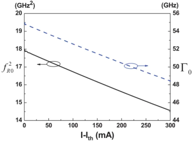
![Fig. 3 illustrates the turn-on delay properties for various injected currents. With the increase of the pump current, the delay time becomes shorter which means that the carrier lifetime is decreased [29]](https://thumb-eu.123doks.com/thumbv2/123doknet/12247955.319807/5.918.92.427.122.685/illustrates-properties-various-injected-currents-increase-lifetime-decreased.webp)
Documents relatifs
This special issue aims to advance this scholarship as an interdisciplinary undertaking, by looking at the relationship between collective identities and the integration of core
dans la forêt de mangrove, les autres espèces observées sont communes au littoral.. Ces peuplements ont été à l’origine de la mosaïque de sociétés existant
- It is the purpose of this paper to study on the one hand, what new features characterise non steady state carrier transport in sub-micron semiconductor devices, and on the other
Indeed, as one decreases the cavity bandwidth (for a fixed value of the mechanical resonance frequency), the effective response time of the mirror becomes comparable to that of
We also note that given a well-known down- conversion process, the nonlocal phase of the daughter photon pair encodes the phase of the pump pulse and is invariant under local
From the analysis of figure 4(a), we thus conclude that in CAP1, when the top gated surface state is charge neutral and the bulk is depleted, the bottom ungated topological
Quantum dynamics calculations of the ground state tunneling splitting and of the zero point energy of malonaldehyde on the full dimensional potential energy surface proposed by Yagi
The correlation between the decay of physiological chromatin regularity and derepression of transcription in Acf mutant embryos suggests that the reduced stringency of DNA packaging
