HAL Id: hal-01299872
https://hal.archives-ouvertes.fr/hal-01299872
Submitted on 8 Apr 2016
HAL is a multi-disciplinary open access
archive for the deposit and dissemination of
sci-entific research documents, whether they are
pub-lished or not. The documents may come from
teaching and research institutions in France or
abroad, or from public or private research centers.
L’archive ouverte pluridisciplinaire HAL, est
destinée au dépôt et à la diffusion de documents
scientifiques de niveau recherche, publiés ou non,
émanant des établissements d’enseignement et de
recherche français ou étrangers, des laboratoires
publics ou privés.
Bing Zhang, Camilla Kärnfelt, Heiko Gulan, Thomas Zwick, Herbert Zirath
To cite this version:
Bing Zhang, Camilla Kärnfelt, Heiko Gulan, Thomas Zwick, Herbert Zirath. A D-Band Packaged
Antenna on Organic Substrate With High Fault Tolerance for Mass Production. IEEE Transactions
on Components and Packaging Technologies, Institute of Electrical and Electronics Engineers, 2016,
6 (3), pp.359 - 365. �10.1109/TCPMT.2016.2519522�. �hal-01299872�
Abstract— A grid array antenna working around 145 GHz is proposed in this paper. The antenna is built on Liquid Crystal Polymer (LCP) and designed for the D-band Antenna-in-Package (AiP) application. The intrinsic softness of the LCP material is a limiting factor of the antenna’s aperture size. A 0.5 mm thick copper core is used to compensate. By doing this, the rigidness of the antenna is effectively improved, compared with an antenna without the copper core. Wet etching is used to realize the patterns on the top and bottom conductor. Compared with a Low Temperature Co-Fired Ceramic (LTCC) counterpart, we obtain a considerable cost reduction with acceptable performance. The proposed antenna has an impedance bandwidth of 136 – 157 GHz, a maximum gain of 14.5 dBi at 146 GHz and vertical beams in the broadside direction between 141 – 149 GHz. The fabrication procedures of the antennas are introduced and a parametric study is carried out which shows the antenna’s robustness against fabrication tolerances like the not well controlled etching rate and the substrate surface roughness. This makes the antenna a promising solution for mass production.
Index Terms — grid array antenna, liquid crystal polymer, antenna-in-package, surface roughness, D-band.
I. INTRODUCTION
HE requirement for mass production of mmWave antennas is a balance between cost and performance. On the one hand, dimensions of the antennas are in the range of tenth of millimeters, which requires sophisticated processes with tight tolerance for stable antenna performance. On the other hand, the considerable cost of such a sophisticated process hinders mass production. Generally, mmWave antennas can be
This work was supported by the Swedish Foundation for Strategic Research (SSF) through the program of ‘RFIC solutions for very high data rate, energy and spectrum efficient wireless THz communication’ and by the Swedish Research Council (VR) through the program of ‘Gigabits at THz frequencies’.
Bing Zhang and Herbert Zirath are with Microwave Electronics Laboratory, Department of Microtechnology and Nanoscience, Chalmers University of Technology, SE-41296, Gothenburg, Sweden (bzhang0609@hotmail.com). Herbert Zirath is also with Ericsson Research, Ericsson AB, SE-41756, Gothenburg, Sweden.
Camilla Kärnfelt is with the Microwave Department of Télécom Bretagne-Institute Mines-Télécom, Brest, France.
Heiko Gulan and Thomas Zwick are with Institute of Radio Frequency Engineering and Electronics (IHE), Karlsruhe Institute of Technology (KIT), 76131 Karlsruhe, Germany.
categorized as on-chip or in-package antennas. Because of the process limit, the implementation cost of on-chip antennas is usually higher than that of in-package antennas. Moreover gain and efficiency of on-chip antennas are normally lower compared to in-package versions. Examples of realized on-chip antennas include a D-band on-chip end-fire Yagi-Uda antenna with 4.7 dBi peak gain and 76 % radiation efficiency based on a 130-nm SiGe BiCMOS process [1]; an on-chip dual dipole antenna with 7 dBi gain and 60 % efficiency implemented on a SiGe BiCMOS process [2]; and a slot antenna of -2 dBi gain and 18 % efficiency by a CMOS process [3]. Besides the limited antenna gain and radiation efficiency, the considerable clean room processing cost is another barrier for mass production. Moreover, an extra package is needed to when integrating the antenna with ICs. To implement mmWave in-package antennas, Low Temperature Co-fired Ceramic (LTCC) and Liquid Crystal Polymer (LCP) are popular choices [4-6]. To give some examples, a laminated waveguide horn antenna [7], a leaky-wave antenna [8] and a slot array antenna [9] have been reported on LTCC. However, in addition to the relatively high cost of the LTCC material and process, the shrinkage of the substrate in the planar scale of around 5 % makes it difficult for mass production.
Compared with LTCC, LCP features low material cost, large processing area and is compatible with a low-cost process like wet etching. The drawbacks of LCP are the low laminating temperature and its intrinsic softness. Though the softness is preferable for conformal devices, it causes detuned mmWave antenna performance when bended. For example a packaged D-band LCP rod antenna of 10.3 dBi has been reported in [10]. Because of the softness of the LCP material, the length of the LCP rod could not be maximized for increased gain. Besides, the softness increases with the temperature, especially when LCP is used for packaging, which gives rise to mechanical tension between the package and the mother board. As a result, the thermal stability of an LCP device should also be considered, when applied for antennas and packages.
This paper introduces a grid array antenna [11-13], of low cost and comparable performance to an LTCC version
published in[14], on LCP substrate for D-band
Antenna-in-Package (AiP) applications. The cost of the antenna is much reduced by the LCP substrate and the wet etching process. The conformal profile of the antenna and package are preferable for consumer electronics. The intrinsic softness of the LCP is compensated by a 0.5 mm thick copper core. The rigidness of the package is also enhanced. Low-cost fabrication procedures are also introduced. A parametric study shows the
A D-Band Packaged Antenna on Organic
Substrate with High Fault Tolerance for Mass
Production
Bing Zhang, Member, IEEE, Camilla Kärnfelt, Student Member, IEEE, Heiko Gulan, Student Member, IEEE, Thomas Zwick, Senior Member, IEEE, Herbert Zirath, Fellow, IEEE
LTCC counterpart [14], the proposed antenna achieves a considerable cost reduction with acceptable antenna performance. This makes it a capable candidate for mass production. The paper is organized as follows. Section II describes the geometry and fabrication procedures of the antenna. Section III compares the simulated and measured performance of the antenna. Section IV conducts the tolerance analysis versus etching rate and conductor surface roughness, which proves the antenna’s potential for mass production. Section V concludes the paper.
II. GEOMETRY OF THE LCPPACKAGED ANTENNA
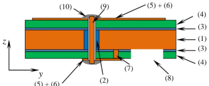
The proposed packaged antenna consists of two Rogers 3850 LCP (εr = 2.9, tanδ = 0.0025) substrates and three metallic layers as shown in Fig. 1. Dimensions of the antenna are (x, y, z) = (10, 10, 0.77) mm. The top and bottom metal layers are 18 µm copper with 5 µm Auto-catalytic Silver Immersion Gold (ASIG). The top and bottom substrates are 100 µm thick. They are bonded by 12 µm Dupont Pyralux LF Sheet Adhesive (εr = 4, tanδ = 0.05) to the 0.5 mm thick copper core. The copper core compensates the intrinsic softness of the LCP substrate. The softness might be preferable for conformal applications but is not desirable for a highly integrated package and a mmWave antenna that require substrate flatness and rigidness. For example, a tiny bendy structure can give rise to the deformation of the antenna’s geometry, which in turn leads to detuned antenna’s performance. Besides, the mechanical tension on the surface, which is brought about by the bendy substrate, would also challenge the adhesion of the package to the mother board. By adopting the 0.5 mm thick copper core, we introduce extra rigidness to compensate the intrinsic softness of the LCP substrate. Another problem is the heat generated by the dissipated power when the antenna is integrated with an active circuit, and then flipped to the mother board. For example, as the temperature increases with the functioning time, the softness of the LCP substrate increases given that it is a thermoplastic material with its lamination temperature at 285°C. This gives rise to a tension on the junction between the packaged antenna and the mother board. The 0.5 mm highly thermal conductive copper core facilitates the dissipation of heat. By adopting the copper core, we minimize the tension between the packaged antenna and the mother board, which is generated by components of different Coefficient of Thermal Expansion (CTE). A clearance via hole of 325 µm is drilled through the copper core and plugged by THP-100 DX1 (εr = 3.6, tanδ = 0.013). The 325 µm diameter of the clearance via is extremely large considering the ball map layout of the D-band RFIC, it is a compromise between the fabrication limitation and impedance matching of the antenna. The characteristic impedance of the coaxial structure formed by (1), (2) and (9) in Fig. 1 is 46.3 Ω. Since the 325 µm diameter clearance via will not be in direct contact with the D-band RFIC, the influence is negligible. A feeding via hole of 75 µm radius goes through the clearance via. By disposing the radiating array and the feeding network apart on each side of the copper core, mutual coupling between the antenna and the chip is minimized.
Fig. 1. Stack-up of the proposed D-band LCP packaged antenna: (1) copper core, (2) THP-100 DX1, (3) adhesive, (4) LCP, (5)+(6) copper + ASIG, (7) grounding via, and (8) chip pocket, (9) feeding via and (10) solder.
Fig. 2 shows the design view of the antenna. In the top view Fig. 2 (a), the radiating grid array is composed of 41 uniform interconnected grids. The working principle of a grid array antenna is explained e. g. in [11-13] and shall not be explained in detail here. The short side of the grid s is 0.72 mm, which is half the guided wavelength. The long side l is 1.44 mm. The width of both the short and long sides is ws = wl = 0.06 mm. As shown in Fig. 2 (e), the short sides of each grid carry in-phase current, pointing to the same direction that contributes to the co-polarization. The current on the long sides are out-of-phase, pointing to the opposite direction, which contributes to the cross-polarization. A circular catch pad of 100 µm radius is designed near the radiating array’s geometrical center for feeding. Fig. 2 (b) shows the bottom view. A pocket of (x, y, z) = (4, 3, 0.112) mm is designed to house the chip. A testing pad with a 100 µm radius circular catch pad for the 75 µm radius feeding via hole is designed for GSG (Ground-Signal-Ground) probe testing or wire bonding to the chip. Usually the wire bonding transition at the D-band will cause significant parasitic and insertion loss. The parasitic inductance can be compensated by extra capacitance, like the increased pad size. The insertion loss lies in the range of 1 ~ 3 dB in the D-band, which is not negligible [14]. However, the contribution of the bond wire insertion loss of a packaged antenna to the system is much less than that of an on-chip antenna, whose radiation efficiency is usually - 6 ~ - 10 dB. As a result, the packaged antenna is more preferable in terms of noise contribution. The test pad is DC-grounded by two grounding vias with 75 µm radius to form the GCPW structure. The clearance between the test pad and the cavity is 50 µm. The square pad arrays on the four corners of the bottom side are designed for flip chip testing. Fig. 2 (c) gives the dimensions of the feeding pad. The inductance of the feeding via is compensated by the catching pad and the section
l2 in Fig. 2 (c). The CWP feed in section l4 has a 50 Ω
impedance. The antenna is matched to the 50 Ω feed impedance via transmission lines through l1, l2, l3 and l4 by a high-low-high-low matching network. When the input signal goes from the testing pad through the feeding coaxial via to the radiating array, the structural discontinuities will cause reflection and radiation, like shown in Fig. 2 (d). This will give rise to Electro Magnetic Compatibility (EMC) complexities when the antenna is used in a highly integrated system, which should be taken care of seriously.
y z (3) (1) (3) (4) (2) (7) (4) (5) + (6) (8)
(a) (b)
(c)
(d)
(e)
Fig. 2. Design view of the proposed D-band LCP packaged antenna: (a) top view, (b) bottom view and (c) zoomed view of the test pad: c = 212 µm, g1 = 30 µm, g2 = 100 µm, l1 = 497 µm, w1 = 139 µm, l2 = 392 µm, w2 = 268 µm, l3 = 349 µm, w3 = 100 µm, l4 = 385 µm, w4 = 70 µm, l5 = 140 µm, w5 = 465 µm and p = 565 µm, (d) cross section view of the E-field distribution at the coaxial transition through the copper core, and (e) current distribution on the grid.
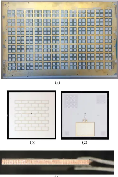
Fig. 3 show photographs of the fabricated antenna. Fig. 3 (a) is the layout view of 336 antennas after one fabrication run on a 45.5 cm × 35.5 cm panel. The finished rate of the process is 95%. Fig. 3 (b) shows the radiating grid array on the top view. On the bottom view of in Fig. 3 (c), the test pad and the chip pocket are shown. From the side view in Fig. 3 (d), the stacked 0.5 mm thick copper core and the LCP substrates can be seen. The fabrication procedures start with the 0.5 mm thick copper core. A via clearance hole of 325 μm radius is firstly drilled, and then filled with THP-100 DX1. The 12 μm thick layers of DuPont Pyralux LF Sheet Adhesive are painted on both sides of the copper core, and heated to 190 ˚C to bond the Rogers 3850 substrates. Patterns of the top and bottom metal layers are realized by wet etching. Laser ablation is used to cut out the chip pocket, the gaps of the testing pad, the 75 μm radius feeding via hole and the 75 μm radius ground via hole. A 5 μm layer of Auto-catalytic Silver Immersion Gold (ASIG) is deposited on the 18 μm thick copper traces to enable wire bonding. The grounding vias are plated by ASIG as well. At last, a copper wire is soldered through the transition hole from the pad to feed the radiating array.
(a)
(b) (c)
(d)
Fig. 3. Photographs of the D-band LCP packaged antenna: (a) layout view of 336 antennas in one fabrication run on a 45.5 cm
catch pad feeding via l1, w1 l2, w2 l3, w3 l4, w4 l5 grounding via x w5 g1 g2 c p y chip pocket short side long side
x y z
III. SIMULATED AND MEASURED ANTENNA PERFORMANCE
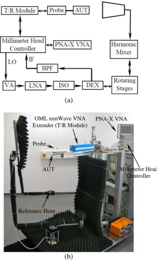
The full-wave Finite Element Method (FEM) simulator Ansoft HFSS is used to simulate the antenna. The fabricated antenna is measured in a far-field setup in Télécom Bretagne-Institute Mines-Télécom and Karlsruhe Institute of Technology [15]. A diagram of the measurement setup is shown in Fig. 4 (a). |S11| of the antenna is measured directly by accessing the GCWP pad of the antenna using a GSG probe, which is connected via a mmWave VNA extender to the PNA. Concerning the far-field measurement, rotating stages move a reference horn antenna around the AUT (Antenna under Test). The received signal is down-converted by a harmonic mixer, split by a diplexer, and then goes through a band-pass filter to the PNA. The LO signal goes from the millimeter head controller with a variable attenuator and an amplifier to ensure the correct LO level at the harmonic mixer. Fig. 4 (b) shows the photograph of the measurement setup.
(a)
(b)
Fig. 4 Measurement setup of the D-band LCP packaged antenna: (a) block diagram and (b) photograph.
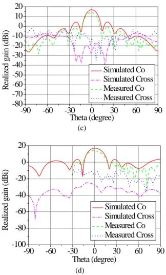
Fig. 5 (a) compares the simulated and measured |S11| of the antenna. In simulation, the -10 dB bandwidth is 137-152 GHz, while in measurement it is 136-157 GHz. Fig. 5 (b) shows the simulated and measured gain. The antenna has the maximum
is 61.8 %. It is comparable with the calculated 67.9 % aperture efficiency of the antenna in [14]. The comparison of the aperture efficiency proves that the proposed antenna features equal performance with low cost. The antenna has vertical beams in the broadside direction between 141 GHz and 149 GHz. Fig 5 (c) and (d) show the radiation patterns at 146 GHz. The antenna is measured to have a 15˚ 3-dB beamwidth and -27 dB cross-polarization in E-plane; while 18˚ 3-dB beamwidth and -40 dB cross-polarization in H-plane. The difference between the simulated and measured results may be caused by fabrication tolerance, which will be investigated in the following section.
130
135
140
145
150
155
160
-20
-15
-10
-5
0
|S
11
| (
d
B)
Frequency (GHz)
Simulated
Measured
(a)130
135
140
145
150
155
160
-6
-4
-2
0
2
4
6
8
10
12
14
16
18
P
eak
r
eal
ized
g
ai
n
(
d
B
i)
Frequency (GHz)
Simulated
Measured
(b) Probe Reference HornOML mmWave VNA Extender (T/R Module)
PNA-X VNA
AUT Millimeter Head Controller
-90
-60
-30
0
30
60
90
-80
-70
-60
-50
-40
-30
-20
-10
0
10
20
R
eal
ized
g
ai
n (
dB
i)
Theta (degree)
Simulated Co
Simulated Cross
Measured Co
Measured Cross
(c)-90
-60
-30
0
30
60
90
-100
-80
-60
-40
-20
0
20
R
eal
ized
g
ai
n
(
d
B
i)
Theta (degree)
Simulated Co
Simulated Cross
Measured Co
Measured Cross
(d)Fig. 5. Simulated and measured performance of the D-band LCP packaged antenna: (a) |S11|, (b) peak realized gain, (c) E-plane radiation patterns at 146 GHz and (d) H-plane radiation patterns at 146 GHz.
IV. FABRICATION TOLERANCE ANALYSIS FOR MASS
PRODUCTION
To satisfy the need for mass production, which requires a balance between cost and performance, wet etching is used to implement the top and bottom conductor patterns for low-cost consideration. However, the dimensional tolerance of wet etching is not always well-controlled. The microscopic inspection shows 10 – 15 µm etching tolerance of the conductors, and the cross-section of the conductor is trapezoid rather than rectangular.
To evaluate the antenna’s vulnerability against the not-well-controlled etching rate, a parametric study is conducted in simulation. The antenna’s input impedance and gain are simulated under the condition that the width of the radiating array varies as ws-20 µm, ws-10 µm, ws, ws+10 µm and ws + 20 µm, representing an over- or under-etching in fabrication. Fig. 6 (a) shows the input matching of the antenna. The input impedance Zin of the antenna is determined by the characteristic impedance Z0 of the conductor trace, while the Z0 of the conductor trace is affected by its width. As a result, the dimensional variation of the conductor trace is reflected by the Zin of the antenna. Frequency shifts of ± 5 GHz can be observed
in Fig. 6 (a), while the antenna’s impedance bandwidth still covers a range of 141-148.5 GHz when the not-well-controlled etching rate is taken into consideration. The antenna is composed of interconnected grids. The frequency shift is caused by the variation of the length of the grid. Widths of both the short and long sides (ws and wl) are affected by the etching rate. As a result, when the ws is changed by the etching rate, the length of the conjunctional long side l is also varied which in turn shifts the operational frequency. The antenna’s impedance bandwidth proves its robustness against the etching rate. As it can be seen in Fig. 6 (b) the antenna’s maximum gain is not much affected by the dimensional deviation, but shifts ± 5 GHz in frequency. This is because the dimensional variation of the grid will shift and vary the gain of each short side, which has the same mechanism as a half-wave dipole. The variation and frequency shift of each short side of the grid contribute to that of the whole antenna.
130
135
140
145
150
155
160
-35
-30
-25
-20
-15
-10
-5
|S
11
| (
d
B)
Frequency (GHz)
ws-20 µm
ws-10 µm
ws
ws+10 µm
ws+20 µm
(a)130
135
140
145
150
155
160
-2
0
2
4
6
8
10
12
14
16
18
P
eak
r
eal
ized
g
ai
n
(
d
B
i)
Frequency (GHz)
ws-20 µm
ws-10 µm
ws
ws+10µm
ws+20µm
(b)Fig. 6 Parametric study of the D-band LCP packaged antenna’s performance against dimensional tolerances given by simulation: (a) |S11| and (b) peak realized gain.
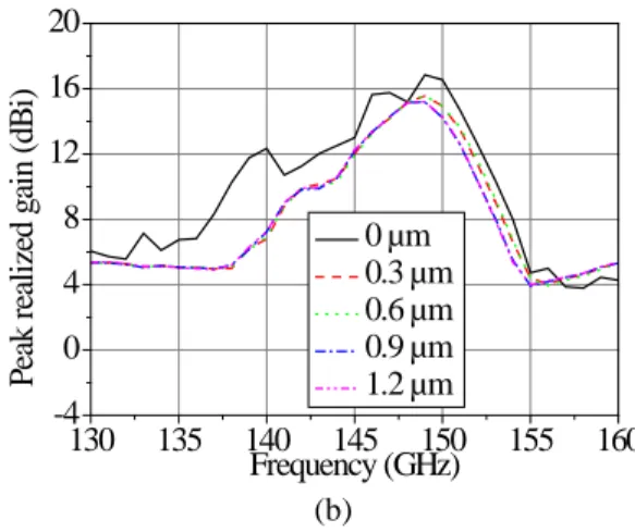
Another influential factor on a microstrip antenna’s performance is the surface roughness. In practice, certain surface roughness is needed to ensure good adhesion between the substrate and the conductor, while the surface roughness is also partly responsible for the conductor loss. Especially when the frequency goes up to the mmWave and the surface
bare LCP substrate, whose copper cladding is chemically etched by the same process as antenna fabrication, is scanned by the AlphaStep500 profilometer under room temperature to deduce the conductor-substrate surface roughness. The root mean square (RMS) surface roughness is 0.3 μm, while the skin depth of 140 GHz electromagnetic waves on copper is 0.175 µm. To investigate the antenna’s vulnerability against surface roughness, a parametric study is conducted. The antenna’s impedance bandwidth and gain are simulated against the surface roughness of the substrate in the range of (0, 1.2) µm with a 0.3 µm step. In Fig. 7 (a), it is reasonable that the increased conductor loss by surface roughness does not deteriorate but improves the input matching of the antenna because of decreased Q factor of the antenna, which is a resonant component. For example in the ideal case of the smooth substrate, the impedance bandwidth of the antenna is 137.5 – 152 GHz. When the surface roughness increases, the impedance bandwidth extends to 135 – 155 GHz. Thus, the antenna’s impedance bandwidth is robust against substrate surface roughness.
In Fig. 7 (b), the increased surface roughness gives rise to decreased antenna gain. According to the equation of surface roughness related to conductor loss [16]
+ = − 2 1 ' 1 2tan 1.4 δ π RMS c c (1)
where c’ is the conductor loss of a rough microstrip line, c is the conductor loss of an ideal microstrip line, RMS is the root mean square of the surface roughness and δ is the skin depth. To give example when the surface roughness is 0.3 μm in Fig. 7 (b), the conductor loss increases by 2.67 dB, which is testified by the 2.3 dB decrement between the antenna’s gain with 0 µm and 0.3 µm surface roughness. When the surface roughness increases to 0.6 µm and keeps increasing, the conductor loss stays stable at twice value of the ideal microstrip line. As a result, the difference between the gain of an ideal LCP antenna and that with surface roughness larger than 0.6 µm is stabilized at 3 dB, which is in accordance with eqn. (1). From the parametric study above, it can be seen that that antenna’s performance is robust against fabrication tolerance of not-well-controlled etching rate and surface roughness, which is a highly appreciated advantage for low-cost mass production.
130 135 140 145 150 155 160 -20 -15 -10 -5 0 |S11 | ( d B) Frequency (GHz) 0 µm 0.3 µm 0.6 µm 0.9 µm 1.2 µm (a) 130 135 140 145 150 155 160 -4 0 4 8 12 16 P eak r eal ized g ai n ( d B i) Frequency (GHz) 0 µm 0.3 µm 0.6 µm 0.9 µm 1.2 µm (b)
Fig. 7 Parametric study of D-band LCP packaged antenna’s performance against substrate surface roughness from simulation: (a) |S11| and (b) peak realized gain.
V. CONCLUSION
This paper demonstrates a low-cost D-band LCP packaged antenna for mass production. The intrinsic softness of the LCP is compensated by a 0.5 mm copper core. Comparing with a LTCC counterpart, a considerable cost reduction is achieved by the proposed antenna due to the low-cost substrate and process. The fabrication procedures are introduced and explained. The simulated antenna performance agrees well with measurement. The antenna’s performance remains stable against fabrication tolerance of the not-well-controlled etching rate and the surface roughness. This makes the antenna preferable for mass production.
VI. ACKNOWLEDGEMENT
The author would like to acknowledge Mr. Raymond Jezequel from Télécom Bretagne-Institute Mines-Télécom for antenna measurement; Dr. Per-Åke Nilsson, Dr. Robin Dahlbäck and Dr. Zhaoyao Zhan from Chalmers University of Technology for surface roughness measurement and photograph taking; Dr. Yinggang Li, Dr. Mingquan Bao, Dr. Jonas Hansryd and Dr. Thomas Emanuelsson from Ericsson for the discussions; Professor Yue Ping Zhang from Nanyang Technological University for the comments.
REFERENCES
[1] W. T. Khan, A. C. Ulusoy, G. Dufour, M. Kaynak, B. Tillack, J. D. Cressler, and J. Papapolymerou, “A D-band micromachined end-fire antenna in 130-nm SiGe BiCMOS Technology,” IEEE Trans. Antennas
Propag., vol. 63, no. 6, pp. 2449-2459, Jun. 2015.
[2] S. Pan, L. Gilreath, P. Heydari, and F. Capolino, “Designs of fully on-chip antennas in (Bi)CMOS technology,” in Proc. IEEE Intl. Workshop
Antenna Technol., Mar. 5-7, 2012, pp. 343-346.
[3] S. Pan and F. Capolino, “Design of a CMOS on-chip slot antenna with extremely flat cavity at 140 GHz,” IEEE Antennas Wireless Propag. Lett., vol. 10, pp. 827-830, Aug. 2011.
[4] Y. P. Zhang and D. Liu, “Antenna-on-chip and antenna-in-package solutions to highly integrated millimeter-wave devices for wireless communications,” IEEE Trans. Antennas Propag., vol. 57, no. 10, pp. 2830-2841, Oct. 2009.
[5] C. E. Patterson, W. T. Khan, G. E. Ponchak, G. S. May, and J. Papapolymerou, “A 60-GHz active receiving switched-beam antenna array with integrated butler matrix and GaAs amplifiers,” IEEE Trans.
[6] C. H. J. Poh, C. E. Patterson, S. K. Bhattacharya, S. D. Philips, N. E. Lourenco, J. D. Cressler, and J. Papaploymerou, “Packaging effects of multiple X-band SiGe LNAs embedded in an organic LCP substrate,”
IEEE Trans. Comp. Packag. Manuf. Technol., vol. 2, no. 8, pp.
1351-1360, Aug. 2012.
[7] B. Cao, H. Wang, Y. Huang, J. Wang, and H. Xu, “A novel antenna-in-package with LTCC technology for W-band application,”
IEEE Antennas Wireless Propag. Lett., vol. 13, pp. 357-360, Mar. 2014.
[8] Y. J. Cheng, Y. X. Guo, X. Y. Bao, and K. B. Ng, “Millimeter-wave low temperature co-fired ceramic leaky-wave antenna and array based on the substrate integrated image guide technology,” IEEE Trans. Antennas
Propag., vol. 62, no. 2, pp. 669-676, Feb. 2014.
[9] J. Xu, Z. N. Chen, X. Qing, and W. Hong, “140-GHz TE20-mode
dielectric loaded SIW slot antenna array in LTCC,” IEEE Trans.
Antennas Propag., vol. 61, no. 4, pp. 1784-1793, Apr. 2013.
[10] N. Saiz, N. Dolatsha, and A. Arbabian, “A 135GHz SiGe transmitter with a dielectric rod antenna-in-package for high EIRP/channel Arrays,” in
Proc. IEEE ICCC, Sep. 15-17, 2014, pp. 1-4.
[11] B. Zhang, “Design and analysis of millimeter-wave packaged grid array antennas on low temperature co-fired ceramics,” LAP Lambert Academic Publishing, Germany: Saarbrücken, ISBN 978-3-659-62443-8, 2014. [12] M. Sun and Y. P. Zhang, “Grid antenna arrays,” Springer International
Publishing AG, Germany: Berlin, ISBN 978-981-4560-75-7, 2015.
[13] M. Sun, Y. P. Zhang, D. Liu, K. M. Chua, and L. L. Wai, “A ball grid array package with a microstrip grid array antenna for a single-chip 60 GHz receiver,” IEEE Trans. Antennas Propag., vol. 59, no. 6, pp. 2134-2140, May 2011.
[14] B. Zhang, H. Gulan, T. Zwick, Y. Li, U. Oderfält, F. Carlsson, and H. Zirath, “Integration of a 140 GHz packaged LTCC grid array antenna with an InP detector,” IEEE Trans. Comp. Packag. Manuf. Technol., vol. 5, no. 8, pp. 1060-1068, Aug. 2015.
[15] H. Gulan, S. Beer, S. Biebold, C. Rusch, A. Leuther, I. Kallfass, and T. Zwick, “Probe based antenna measurements up to 325 GHz for upcoming millimeter-wave applications,” in Proc. IEEE Int. Workshop Antenna
Technol. (iWAT2013), Karlsruhe, Germany, Mar. 4-6, 2013, pp. 228-231.
[16] E. O. Hammerstad and F. Bekkadal, A Microstrip Handbook, ELBA report, STF 44 A74169, University of Trondheim, Norway, 1975, pp 98-110.
Bing Zhang (S’09-M’13) was born in Shanxi, China.
He received the B.E. degree from the Civil Aviation University of China 2004, the M.E. degree from Shanxi University 2008, both in electrical and electronic engineering, and the Ph.D. degree from the School of Electrical and Electronic Engineering, Nanyang Technological University. He has been working as a post-doctoral researcher since November 2012 with the Microwave Electronics Laboratory (MEL), Department of Microtechnology and Nanoscience (MC2), Chalmers University of Technology. He has been working as visiting scholar at University of Nice Sophia Antipolis in May 2012 and at Télécom Bretagne in November 2014 and April 2015. His research interests include design and co-design of RF passive and active devices, packaging of RF devices and the application of 3D printing technology for mmWave applications. He is the recipient of the Foxconn Scholarship in 2008, the Singapore Ministry of Education Scholarship from 2009 to 2012, the Dragon Venture Award in 2012, the Best Student Paper Award of the Asia-Pacific Conference on Antennas and Propagation in 2012, and the Young Scientist Award 2013 of International Union of Radio Science (URSI, Commission B). He is the TPC member and TPC chair of several international conferences. He serves as a viewer for journals including IEEE
Transactions on antennas and propagation, IEEE Transactions on Terahertz Science and Technology, IEEE Transactions on Microwave Theory and Techniques and IEEE Microwave and Wireless Components Letters. He has
authorized one book chapter, one book and two patents. He is a consultant for Sunrise Co., Ltd. (Guangzhou, China), in developing mobile base station antennas. He is the Chief Technology Officer (CTO) of Blue Ocean Information Technology Co., Ltd. (Wuhan, China), in developing wearable electronic devices.
Camilla Kärnfelt received her M.Sc. degree in
engineering physics at Chalmers University of Technology, Göteborg, Sweden in 2001. She has held positions as a pre-production engineer specialized in microwave hybrids both at Ericsson (1987-2001) and at Optillion (2001-2002). From 2002 to 2007 she worked at
Chalmers University of Technology at the Microwave Electronics Laboratory as a Research Engineer specializing in millimeter wave MMIC design and packaging. Since July 2007 she is employed at the Microwave Department at Institut Mines Télécom/Télécom Bretagne as an assistant professor and is currently pursuing her PhD in the field of mm-wave packaging. She is a member of the CNRS laboratory Lab-STICC UMR 6285 since 2009.
Heiko Gulan (SM’99) received the Dipl.-Ing. (FH)
degree from the University of Applied Science Esslingen, Germany, in 2008, and the Dipl.-Ing. in electrical engineering degree from the Karlsruhe Institute of Technology (KIT), Germany, in 2010. Since 2011, he works as a Research Staff Member at the Institut fur Hochfrequenztechnik und Elektronik (IHE), where he is currently working toward the Dr.-Ing. degree. His research interests include millimeter and submillimeter-wave antennas, lens antenna design, and millimeter-wave packaging. He also has experience in designing waveguide filter components for spaceborne applications.
Thomas Zwick (S’95–M’00–SM’06) received the
Dipl.-Ing. (M.S.E.E.) and the Dr.-Ing. (Ph.D.E.E.) degrees from the Universität Karlsruhe (TH), Germany, in 1994 and 1999, respectively. From 1994 to 2001 he was a research assistant at the Institut für Höchstfrequenztechnik und Elektronik (IHE) at the Universität Karlsruhe (TH), Germany. In February 2001 he joined IBM as research staff member at the IBM T. J. Watson Research Center, Yorktown Heights, NY, USA. From October 2004 to September 2007, Thomas Zwick was with Siemens AG, Lindau, Germany. During this period he managed the RF development team for automotive radars. In October 2007, he became a full professor at the Karlsruhe Institute of Technology (KIT), Germany. He is the director of the Institut für Hochfrequenztechnik und Elektronik (IHE) at the KIT. He is author or co-author of over 200 technical papers and 20 patents. His research topics include wave propagation, stochastic channel modeling, channel measurement techniques, material measurements, microwave techniques, millimeter wave antenna design, wireless communication and radar system design. Thomas Zwick received over 10 best paper awards on international conferences. He served on the technical program committees (TPC) of several scientific conferences. In 2013 Dr. Zwick was general TPC chair of the international Workshop on Antenna Technology (iWAT 2013). He also is TPC chair of the European Microwave Conference (EuMC) 2013. Since 2008 he has been president of the Institute for Microwaves and Antennas (IMA). T. Zwick became selected as a distinguished IEEE microwave lecturer for the 2013 – 2015 period with his lecture on “QFN Based Packaging Concepts for Millimeter-Wave Transceivers”.
Herbert Zirath (M' 86-SM'08-F'11) was born in Göteborg, Sweden, on March 20, 1955. He received the M. Sc and Ph. D. degree in electrical engineering from Chalmers University, Göteborg, Sweden, in 1980 and 1986, respectively. From 1986 to 1996 he was a researcher at the Radio and Space Science at Chalmers University, engaged in developing a GaAs and InP based HEMT technology, including devices, models and circuits. In the spring-summer 1998 he was research fellow at Caltech, Pasadena, USA, engaged in the design of MMIC frequency multipliers and Class E Power amplifiers. He is since 1996 Professor in High Speed Electronics at the Department of Microtechnology and Nanoscience, MC2, at Chalmers University. He became the head of the Microwave Electronics Laboratory 2001. At present he is leading a group of approximately 40 researchers in the area of high frequency semiconductor devices and circuits. His main research interests include MMIC designs for wireless communication and sensor applications based on III-V, III-N, Graphene, and silicon devices. He is author/co-author of more than 530 refereed journal/conference papers, and holds 5 patents. He is research fellow at Ericsson AB, leading the development of a D-band (110-170 GHz) chipset for high data rate wireless communication. He is a co-founder of Gotmic AB, a company developing highly integrated frontend MMIC chip-sets for 60 GHz and E-band wireless communication.