W*M UNIVERSITY DE
m SHERBROOKE
Universite de SherbrookeFaculte de genie
Departement de genie electrique et genie informatique
OPTIMISATION TEMPORELLE DE CIRCUITS LOGIQUES
PAR L'UTILISATION DE TAMPONS
Memoire de maitrise es sciences appliquees
Specialite: genie electrique
Amir Hossein RABBANI
1*1
Library and
Archives Canada
Published Heritage
Branch
395 Wellington Street Ottawa ON K1A0N4 CanadaBibliotheque et
Archives Canada
Direction du
Patrimoine de I'edition
395, rue Wellington Ottawa ON K1A0N4 CanadaYour file Votre reference ISBN: 978-0-494-37929-5 Our file Notre reference ISBN: 978-0-494-37929-5
NOTICE:
The author has granted a
non-exclusive license allowing Library
and Archives Canada to reproduce,
publish, archive, preserve, conserve,
communicate to the public by
telecommunication or on the Internet,
loan, distribute and sell theses
worldwide, for commercial or
non-commercial purposes, in microform,
paper, electronic and/or any other
formats.
AVIS:
L'auteur a accorde une licence non exclusive
permettant a la Bibliotheque et Archives
Canada de reproduire, publier, archiver,
sauvegarder, conserver, transmettre au public
par telecommunication ou par Plntemet, prefer,
distribuer et vendre des theses partout dans
le monde, a des fins commerciales ou autres,
sur support microforme, papier, electronique
et/ou autres formats.
The author retains copyright
ownership and moral rights in
this thesis. Neither the thesis
nor substantial extracts from it
may be printed or otherwise
reproduced without the author's
permission.
L'auteur conserve la propriete du droit d'auteur
et des droits moraux qui protege cette these.
Ni la these ni des extraits substantiels de
celle-ci ne doivent etre imprimes ou autrement
reproduits sans son autorisation.
In compliance with the Canadian
Privacy Act some supporting
forms may have been removed
from this thesis.
Conformement a la loi canadienne
sur la protection de la vie privee,
quelques formulaires secondaires
ont ete enleves de cette these.
While these forms may be included
in the document page count,
their removal does not represent
any loss of content from the
thesis.
Canada
Bien que ces formulaires
aient inclus dans la pagination,
il n'y aura aucun contenu manquant.
Circuit delay optimization by buffering the logic gates
PREFACE
As devices shrink, deep submicron designs demonstrate the increasing importance of interconnect delay on the circuit performance. In order to reduce interconnect delay and help driving large fanout, buffer insertion needs to be performed during logic and physical synthesis. This optimization activity is often based on dynamic programming. In this dissertation, using the branch-and-bound technique, the problem for the specific case of buffering balanced trees is solved, where all loads have identical required time and input load capacitance. Necessary mathematical and data structural elements are provided to take into account a variety of design issues such as topology, buffer library and phase-shifting in the presence of inverting buffers. Combining dynamic programming and branch-and-bound techniques, a hybrid method is presented to improve runtime while memory consumption remains reasonably low. The underlying mathematical and algorithmic concepts given in this thesis can be used to generalize the proposed buffering method to produce a buffer tree for a set of different loads with different required time and capacitance.
Optimisation temporelle de circuits logiques
par ['utilisation de tampons
RESUME
Avec la miniaturisation actuelle, les circuits demontrent de plus en plus l'importance des delais d'interconnexion. Afin de reduire ce delai, l'insertion de tampons doit etre effectuee durant la synthese logique et la synthese physique. Cette activite d'optimisation est souvent basee sur la programmation dynamique. Dans ce memoire, la technique branch-and-bound est utilise et le probleme pour le cas specifique d'arbres de tampons equilibres est resolu, ou toutes les charges ont un temps requis et une capacite identique. Une analyse mathematique est faite pour tenir compte d'une variete de questions de conception telles que la topologie, la bibliotheque de tampons , et le changement de phase en presence d'inverseur. En combinant la programmation dynamique et les techniques branch-and-bound, une methode hybride est presentee qui ameliore le temps d'execution tout en conservant une utilisation de memoire raisonnable. Les concepts mathematiques et algorithmiques fondamentaux utilises dans ce memoire peuvent etre employes pour generaliser la methode proposee pour un ensemble de charges avec des capacites et des temps requis differents.
ACKNOWLEDGEMENTS
The author wishes to thank several people. I would like to thank Dr. Mailhot for his help, expert insight and valuable guidance which made this thesis an enjoyable experience. I would also like to thank Ali Shanian whose support and true friendship helped me a lot through this Master's project. Last but not least, I would like to thank all my friends, in particular Behnam Mostajeran and Zohreh Rafiei, for being beside me in difficulties and happiness.
To my parents:
Bijan Rabbani Shahla Kamuei
TABLE OF CONTENTS
1 INTRODUCTION 1
1.1 BACKGROUND AND MOTIVATION 1 1.2 CONTRIBUTIONS OF THE THESIS 2
1.3 ORGANIZATION 3
2 OVERVIEW OF SYNTHESIS PROCESS & PREVIOUS WORK 4
2.1 REVIEW OF BUFFERING CONCEPTS 4
2.2 PREVIOUS WORK 17
3 BALANCED BUFFERING ...27
3.1 BALANCED BUFFERING APPLICATIONS: FACTS AND POTENTIALS 28
3.2 STATEMENT OF THE PROBLEM 30
3.3 METHOD.. 30 3.4 ALGORITHM 37 3.5 SOLUTION LIST 39 3.6 BALANCED SUB-TREES 40 3.7 BUFFER SELECTION 44 3.8 HANDLING THE INVERTERS 47 3.9 EXPERIMENTAL RESULTS < 50
3.10 SUMMARY 53
4 MIXED METHOD ..54
4.1 SUITABLE STRUCTURE FOR MEMORY REUSE 55
4.2 MIXED METHOD ALGORITHM 60 4.3 WHEN SHOULD MEMORY REUSE B E PERFORMED? 61
4.4 SOLUTION LIST PRUNING 64
4.5 SEARCH SPACE 66 4.6 MORE SPEEDUP TECHNIQUES 80
4.7 EXPERIMENTAL RESULTS ; 84
4.8 SUMMARY 89
CONCLUSION & FUTURE WORK ...91
APPENDICES 95 APPENDIX A 96
APPENDIX B 104
PROOF OF THE BEST BUFFER EXISTENCE 104
APPENDIX C 114
FINDING THE BEST BUFFER 114
TABLE OF FIGURES
Figure 2-1 Inverting and non-inverting buffer . 5
Figure 2-2 Two different implementations for an inverter 5 Figure 2-3 Modeling the buffer insertion problem 7
Figure 2-4 Circuit synthesis stages 8 Figure 2-5 Buffering in the circuit synthesis steps... 9
Figure 2-6 Logic synthesis stages 10 Figure 2-7 Splitting the fanouts of a gate into several parts 11
Figure 2-8 Buffering during logic synthesis 12 Figure 2-9 Dividing less critical fanouts with buffers 13
Figure 2-10 Balanced Load Decomposition 13 Figure 2-11 The dominance of interconnect delay 14 Figure 2-12 Physical synthesis procedure 16 Figure 2-13 Van Ginneken's algorithm 18 Figure 2-14 A routing grid graph and a buffered minimum Elmore delay path 23
Figure 3-1 Balanced buffering versus a typical buffering problem 28
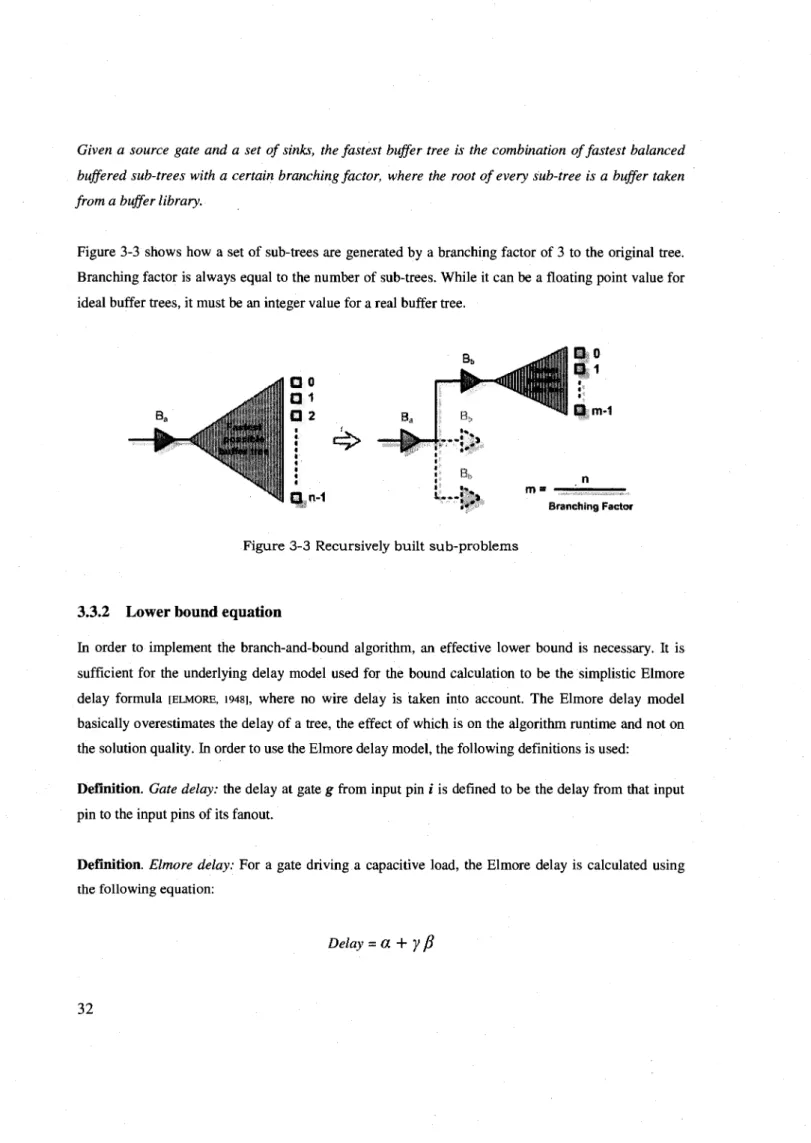
Figure 3-2 Clock tree construction 29 Figure 3-3 Recursively built sub-problems 32 Figure 3-4 Calculating Elmore delay for a given buffer tree 33
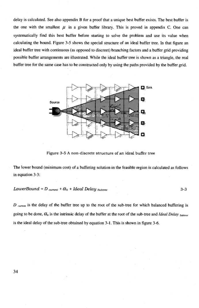
Figure 3-5 A non-discrete structure of an ideal buffer tree 34
Figure 3-6 Lower bound calculation 35 Figure 3-7 Feasible region as a directed acyclic graph 36
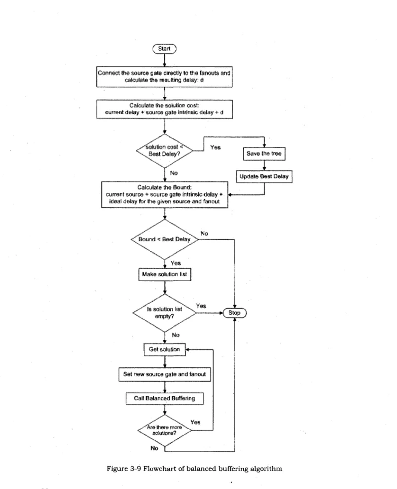
Figure 3-8 Search space graph 37 Figure 3-9 Flowchart of balanced buffering algorithm 38
Figure 3-10 Saving and reconstructing the best buffer tree 39
Figure 3-11 A generic solution structure 40 Figure 3-12 Splitting a tree with a fanout number of 10 in 3 different ways 41
Figure 3-13 The specific case of partially balanced sub-trees : 41
Figure 3-14 3 ways of making partially balanced sub-trees for 17 fanouts 42
Figure 3-15 Legal divisors of 15 43 Figure 3-16 All possible sub-trees for a fanout of 15 44
Figure 3-18 Single wire buffering illustrating theorem 2 46 Figure 3-19 Two different sub-problems leading to a negative-phase sub-tree 47
Figure 3-20 A hybrid solution list... 48 Figure 3-21 Two connected search spaces with different priorities 49
Figure 3-22 Curve-fitting on an arbitrary set of buffering problem runtime 53
Figure 4-1 An example of common sub-problem 56 Figure 4-2 branch-and-bound vs. dynamic programming 57 Figure 4-3 Search space structure for a balanced buffering problem 57
Figure 4-4 Combining two methods in solving a common sub-problem 58 Figure 4-5 Mixed method flowchart ." : 60
Figure 4-6 Basic solutions application 62 Figure 4-7 Setting real delays and sorting the solutions when making a solution list.... 63
Figure 4-8 A sub-problem being updated 64 Figure 4-9 Pruning a positive-phase list 65 Figure 4-10 Pruning a negative-phase list 66
Figure 4-11 Solution types 67 Figure 4-12 2-dimensional coordinate .68
Figure 4-13 Solution list access key 68 Figure 4-14 Usage number distribution for the given example 70
Figure 4-15 A binary search tree with look-up tables inside each node 71
Figure 4-16 Filling up a dynamic look-up table 72 Figure 4-17 An example of push-up function 74 Figure 4-18 Push-up operations for a chain of equally weighted nodes 75
Figure 4-19 The structure of the defined node 76 Figure 4-20 Defining balancing property '. 77
Figure 4-21 Example of see-saw-up function 78 Figure 4-22 Existence of a possible m 80 Figure 4-23 Meeting the same sub-problem through different paths 81
Figure 4-24 Solution jumping for a positive phase solution list 83 Figure 4-25 Memory tracking for a problem with a fanout number of 300 86
Figure 4-26 The effect of the pruning operation on memory usage 87
Figure 4-27 Released memory when using pruning 88 Figure 4-28 Curve-fitting on an arbitrary set of buffering problem runtime 89
Figure A-l Zero level buffering 97 Figure A-2 One level buffering 97
Figure A-3 Two level buffering 99 Figure A-4 K level buffering 100 Figure B-l The proof procedure using Lagrange Multipliers 105
LIST OF TABLES
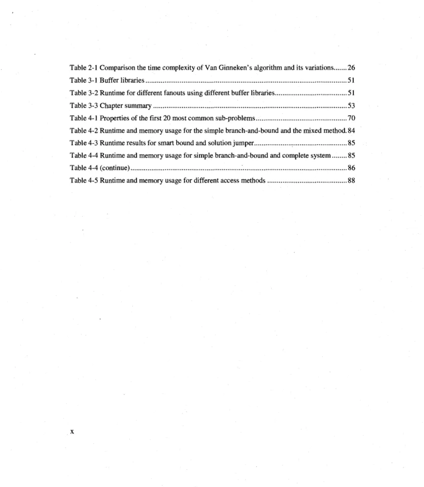
Table 2-1 Comparison the time complexity of Van Ginneken's algorithm and its variations 26
Table 3-1 Buffer libraries 51 Table 3-2 Runtime for different fanouts using different buffer libraries 51
Table 3-3 Chapter summary 53 Table 4-1 Properties of the first 20 most common sub-problems 70
Table 4-2 Runtime and memory usage for the simple branch-and-bound and the mixed method. 84
Table 4-3 Runtime results for smart bound and solution jumper 85 Table 4-4 Runtime and memory usage for simple branch-and-bound and complete system 85
Table 4-4 (continue) 86 Table 4-5 Runtime and memory usage for different access methods 88
Chapter 1
I N T R O D U C T I O N
1.1 Background and Motivation
In modern integrated circuits a logic gate often has to drive very large fanouts. This is due to the fact that during logic synthesis, where generating common expressions is needed to compact the circuit by reducing the number of logic gates, large fanouts are also produced. This is a crucial problem because a logic gate driving large fanouts dramatically slows down the circuit. On the other hand, there are many places where timing is so crucial that one has to make sure that the signals are traveling the circuit as quickly as possible, such as making clock trees, multiplexers, etc. Buffering is one common solution to these problems and is addressed during this dissertation. A new buffering method has been proposed and its efficiency is proved through a number of well-staged testing scenarios. The goal of the presented method is to construct the fastest buffer tree, i.e. a buffer tree by which signals can travel from a logic gate to its fanouts as quickly as possible.
A number of buffering methods have been suggested in the literature (see chapter 2). While these methods are efficient in terms of runtime and memory, none of them guarantees optimality. One often has to compromise runtime and memory consumption at the cost of solution quality. In this dissertation, a buffering method is proposed which produces the optimum solution for a specific class of buffering problems where all fanouts are identical in terms of input capacitance and required arrival time. The presented algorithm is significantly fast and needs very small memory. In constructing the buffer tree, no routing constraint is imposed on the tree structure. This is mainly because there are many applications where timing objectives dominate the geometrical objectives (such as designing a clock tree). In chapter 3, it is shown how one can take advantage of the special structure of this class of buffering problems to nicely model and solve them. The properties of the problem allow using branch-and-bound algorithm, which guarantees the optimality by nature. Other than optimality, one has to make sure that the solution is produced quickly and the calculations are done with a reasonable amount of memory. Therefore, a number of optimization techniques have been introduced in chapter 4 to improve the performance of the buffering algorithm proposed in chapter 3. It is going to be discussed how the solution space being explored by the buffering algorithm is characterized in such a
way that one can avoid redundant calculations by storing and retrieving common solutions. This optimization technique results in faster runtime. Some modifications on the branch-and-bound algorithm have been also put together to speed-up the buffer tree construction. In industrial scale problems, where synthesis tools have to deal with logic gates having hundreds of thousands of fanouts, memory consumption becomes a bottleneck. To avoid any memory overload in real applications, a new group of binary trees have been designed in this dissertation to help memory consumption remain within a reasonable range. A unique feature of those binary trees is the ability to modify the tree structure based on the way it is used, i.e. providing faster access times for the nodes used more frequently. This new class of binary trees, its properties, implementation and applications is going to be discussed more in details in chapter 4.
1.2 Contributions of the Thesis
In this thesis, a new balanced buffering method along with a number of speed-up techniques has been developed to address the buffering problem from a different perspective. The main contributions are listed as follows:
1- An efficient way of balanced buffering using branch-and-bound algorithm: While most of today's buffering techniques are based on dynamic programming, a new and effective method is proposed based on the branch-and-bound technique. Characterizing the problem from a mathematical point of view, the problem for the specific case of buffering balanced trees is solved, where all loads have identical required time and input load capacitance. This new method is called balanced buffering. As opposed to many buffering methods, the presented balanced buffering algorithm guarantees solution optimality and can handle several design issues simultaneously, such as buffer tree topology, phase shifting in the presence of inverters and buffer library. Also, the underlying concepts are provided for a generalized version of the proposed algorithm to solve the buffering problem for a set of different load capacitances and required times.
2- Speed up techniques for the proposed balanced buffering algorithm: To obtain faster search time for the proposed balanced buffering technique three efficient approaches are introduced for the first time in this thesis: mixed branch-and-bound and dynamic programming (or simply mixed method), smart bound and solution jumper. Applying these speed-up techniques, runtimes up to 60,000 times faster have been achieved for the simple balanced buffering
algorithm, which is a significant contribution to the CPU cost of the buffer tree construction method. While mixed method and smart bound are introduced to specially improve the runtime of balanced buffering, they can be applied to any similar problem where the efficiency of the branch-and-bound algorithm is affected by the existence of common sub-problems in the search space.
Self-reorganizing binary search trees: One of the speed-up techniques, the mixed method, needs to keep the results of solving each sub-problem in order to prevent redundant calculations during search traversal. Such approach requires a simple yet efficient structure to maintain and access the solution lists information in the memory. Lazy weight and perfectly balanced binary search tree, two new classes of dynamic search trees, are proposed for the first time in this thesis to improve the access time of those solution lists. Keeping record of each node usage number, they restructure themselves such that the nodes with higher access number move toward the root of the binary tree. This provides faster access time for highly shared sub-problems which generally improves the balanced buffering algorithm runtime.
1.3 Organization
The thesis is organized as follows. After a short introduction to the work addressed in this dissertation in chapter 1, basic buffering concepts, circuit synthesis stages and previous work in this field are introduced in chapter 2. Balanced buffering algorithm and its analysis are presented in chapter 3. Chapter 4 discusses the speed-up methods to improve the runtime of balanced buffering. Finally, a summary of current work and possible directions of future work is given in chapter 5.
Chapter 2
»
O V E R V I E W OF S Y N T H E S I S
P R O C E S S & P R E V I O U S WORK
In this chapter basic buffering concepts are introduced and a number of widely used buffer insertion techniques are presented. In order to understand how and where buffer tree construction is applied in the circuit design process, in section 2.1 different stages of circuit synthesis are explained and buffer tree construction is addresses at logic and physical synthesis stages. In section 2.2, major buffer insertion techniques are studied. The applications of these techniques encompass area and delay optimization in general, and physical effects such as wire capacitance, wire inductance and the effect of placement and routing in particular.However, it should be pointed out that the buffering method proposed in this dissertation is new and is not an extension of any previously presented buffering method. Yet, reviewing these methods provides insight necessary for understanding the work that has been done in this dissertation.
2.1 Review of Buffering Concepts
2.1.1 What is a buffer?
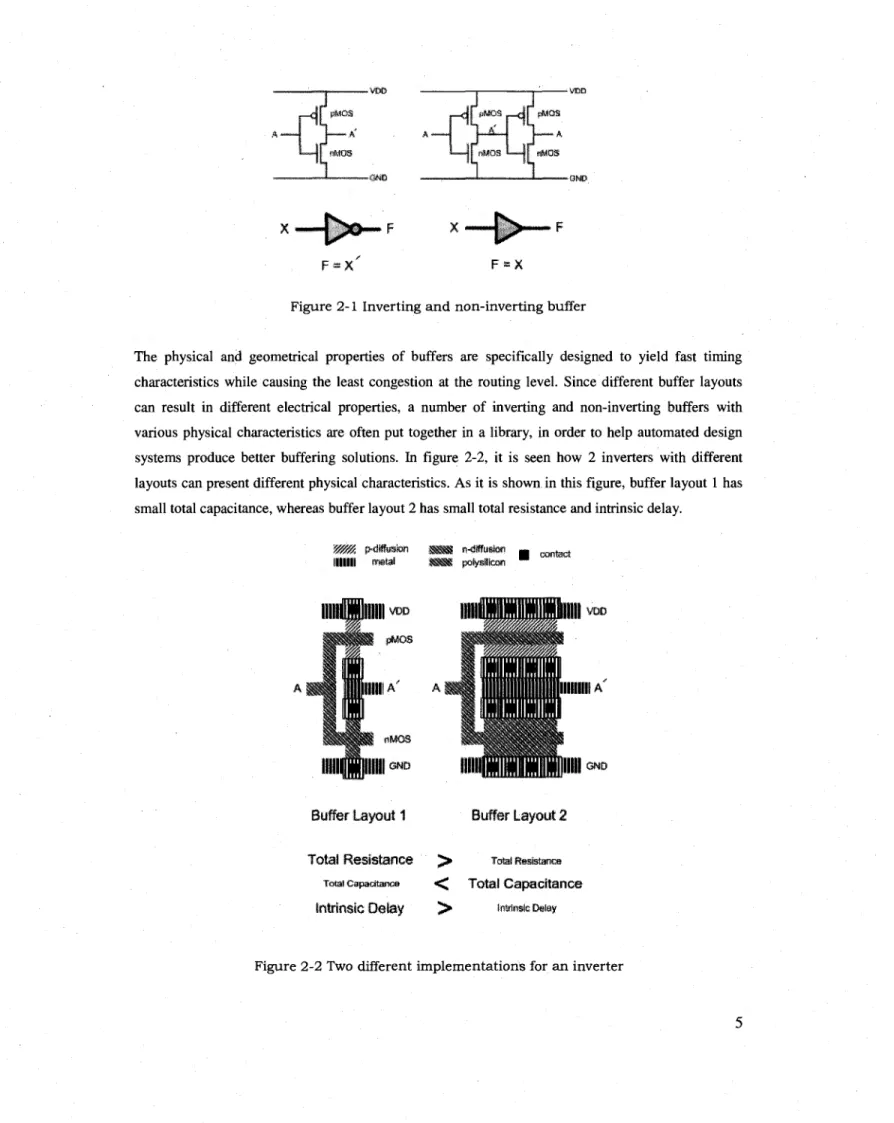
A buffer is an amplifying element placed along the wires and between the logic blocks to help decoupling large loads and regenerating degraded signals. Though a buffer is conventionally known as a neutral logic gate that has no effect on the logic values it transmits, its definition in the domain of circuit synthesis has been extended to also include the inverters. In fact, a non-inverting buffer is a logic-gate compound of 2 contiguous inverters. As the most basic logic unit, inverters are generally smaller and faster than non-inverting buffers. However, the problem of phase-shifting in the presence of inverters makes many buffering algorithms only use non-inverting buffers. Nevertheless, solutions to a buffering problem can still contain inverters as long as the problem of phase-shifting is correctly handled. The symbolic forms of inverting and non-inverting buffers along with their circuits and logic function are shown in figure 2-1.
P S m * c V mi, niiinif^h
-F = X F = X
Figure 2-1 Inverting and non-inverting buffer
The physical and geometrical properties of buffers are specifically designed to yield fast timing characteristics while causing the least congestion at the routing level. Since different buffer layouts can result in different electrical properties, a number of inverting and non-inverting buffers with various physical characteristics are often put together in a library, in order to help automated design systems produce better buffering solutions. In figure 2-2, it is seen how 2 inverters with different layouts can present different physical characteristics. As it is shown in this figure, buffer layout 1 has small total capacitance, whereas buffer layout 2 has small total resistance and intrinsic delay.
p-dffltalon metal n-#tetan potytllcan JH contact:
m
xHim
11
11
Firtffi111!
\>> Rinui \II
MI ^ • • i tMl
TOO IIIIIIIIIA GNDBuffer Layout 1 Buffer Layout 2
T o t a l R e s i s t a n c e * > Tsfel Resistance
Total capadtancs < | Total Capacitance Intrinsic D«Iay > inwnsfcrwajr
A buffer library provides the physical and geometrical diversity required in constructing a buffer tree. This diversity helps choosing the best buffer configuration for the physical characteristics of the given buffering problem. As a consequence of different layout design, a buffer [ALPERT et ai, 2000]:
1) May have a relatively high delay when driving a small load, but a relatively low delay when driving a large load. Such a buffer usually is not a single gate, but rather a series of cascading buffers.
2) May be relatively fast for a large range of loads, but it may have a high input capacitance which increases the delay of the previous stage. This is typically true of large inverting buffers.
3) May have a low input capacitance, which is useful for decoupling a sub-tree that connects non-critical sinks, but the buffer may not have enough strength to drive the entire load that it needs to decouple.
4) May be designed for high noise margins or low power, but perhaps not the best performance.
Hence, many buffering algorithms are designed based on buffer selection techniques. Some of them will be introduce in section 2.2.
2.1.2 How to model a buffering problem
Buffers are typically inserted along the wires and at certain predefined places called legal positions. Legal positions are reserved empty blocks that are specified during the physical synthesis stage (physical synthesis will be introduced in section 2.1.3). Putting a series of buffers at these legal positions forms a buffer tree. An example of buffer tree is shown in figure 2-3. In this figure legal positions are shown by dashed triangles placed along a given routing topology between a source gate and 10 sinks (fanouts). To construct the best buffer tree, one has to decide which empty blocks must be filled out by what type of buffer. This also means that some legal positions can be left empty in order to make the best buffer tree. The number of legal positions in a given routing topology can vary with the physical design restrictions. This problem has been addressed by a number of researches that will be discussed in section 2.2.
s, A \ 7 Sink
1
Source '-,-1 '-,-1 wa< S,r,L
is. Legal S LS^ Buffering rL; u" Position V iS3Figure 2-3 Modeling the buffer insertion problem
Different levels of circuit design process shall be discussed now in order to understand when and how buffer insertion is used in circuit delay optimization procedure.
2.1.3 Circuit Synthesis Stages
In the mid 80's, several academic and commercial systems (Such as BooleDozer by IBM and Encounter RTL Compiler by Cadence) were put together to address the problem of designing ever more complex digital circuits. In the early 90's, when those systems matured and were widely used, their focus broadened from initial optimization of area and delay to encompass power dissipation, testability and physical effects such as wire capacitance, wire inductance, and the effect of placement and routing on delay. Several automatic systems have been developed to help designing faster circuits and make optimization methods more efficient. These automatic systems are all based on 3 main levels, as illustrated in figure 2-4. In High Level Synthesis, the circuit functionality and the input-output behavior is designed' using a high-level hardware description language (HDL). This functionality is then transformed to a netlist in Logic Synthesis followed by technology mapping. In Physical Synthesis, the netlist is transformed into networks of transistors and interconnects and then it is fabricated. While devices shrink in size, meeting the area, time and power consumption objectives becomes more and more critical. As a result, one has to iterate between these three synthesis levels until the cost and speed targets are met.
Figure 2-4 Circuit synthesis stages
2.1.4 Different levels of buffering
As legal positions for buffer insertion are specified in physical synthesis, buffering was originally considered as a post-layout optimization method. However, due to the importance of timing requirements, in modern circuit synthesis tools buffering is done during logic synthesis and then is re-optimized together with physical synthesis. In addition, there are some considerations during high-level synthesis to make buffering a more effective optimization technique in logic and physical synthesis. The situation of buffering in the circuit design sequences is illustrated in figure 2-5. During logic synmesis and when timing properties of the circuit are found, buffer insertion is applied to improve the circuit speed (black box in figure 2-5). Then during placement and routing steps the buffering solution provided by logic synthesis is re-optimized (grey boxes in figure 2-5). This is done at the local placement and detailed routing steps. A number of iterations between high-level, logic and physical take place until the best solution is found.
if
~+
Syntactic Analysis Scheduling Resource Allocation , — p Restructuring Retiming0
0
'•V
—jw 2-level Synthesis Multi-level Synthesis Placement Routing Core Extraction Global: Floorplan H Global: VDD, VSS, BUSFigure 2-5 Buffering in the circuit synthesis steps.
Grey boxes indicate buffering considerations during physical synthesis [MAILHOT, 2005] During the next two sub-sections some optimization problems in logic and physical synthesis will be examined where buffering techniques play a major role in resolving them.
2.1.5 Buffering in logic synthesis
Using an RTL (Register Transfer Language) description as an entry, logic synthesis generates a structural view of a logic-level model and converts this data structure into a network of generic logic cells, called netlist. The synthesis process consists of a sequence of optimization steps, the order and nature of which depend on the chosen cost function-area, speed, power, testability, or some combination. Typically, logic optimization systems divide the task into the following steps [SMITH,
1) A technology independent phase, where the input RTL is parsed (also called analysis) and translated (also called elaboration) to a data structure. This data structure is converted into a network of generic logic cells.
2) Next is the logic optimization phase where the logic is optimized using a number of Boolean or.algebraic manipulation techniques. Many optimization algorithms can be employed here based on the logic involved (combinational or sequential). This step attempts to improve this technology-independent network under the control of the designer. The output of this stage is an optimized, but technology-independent logic network.
3) Further is technology-mapping (also called logic-mapping) phase, where the synthesizer maps the optimized logic to a specified technology-dependent target cell library. This phase takes into account the properties of the intended implementation architectures. The technology-independent description resulting from the earlier phases is thus translated into a gate netlist.
A schematic logic synthesis process is shown in figure 2-6.
Figure 2-6 Logic synthesis stages
We now explain a very common but crucial problem that must always be handled in logic synthesis, and it will be discussed how and at which level buffer insertion can help the situation. Some basic concepts [CARRAGHER and CHENG, 1995] will be defined that are important in the rest of this thesis:
Definition 1. Arrival Time: the actual arrival time ag of gate g is the latest time for which
a valid signal will be produced by g for its fanouts.
Definition 2. Required Time: the required time r„ of gate g is the latest time for which a valid signal is needed on g's fanouts.
Definition 3. Slack: the slack of gate g, Sg, is the difference between its required time and its arrival time, or Sg = rg - ag. The slack of a gate represents how well the timing 10
requirements are being met at that gate, if its slack is positive, and how poorly those requirements are not being met at that gate, if the slack is negative.
Definition 4. Critical Path: path of smallest slack (usually negative) from primary inputs to primary outputs.
During certain logic synthesis steps, some gates with very large fanout are produced, as a result of sharing logic functions. A gate which has to drive many others can significantly slow down the whole circuit, if it is located on the critical path. Fanout optimization in logic synthesis addresses the problem of distributing an electrical signal to a set of sinks with known loads and required times so as to maximize the required time at the signal driver (root of the net). Interconnect delay is not incorporated in this operation because the locations of sinks are not known at this stage. There are two main methods to break large fanouts into smaller portions: splitting and buffer insertion.
One solution to the fanout problem is to split the fanouts of a gate into several parts, each of which driven by a copy of the original gate. To this end, gate duplication is applied to maintain the main logic function while helping a fair load distribution. An example of splitting fanouts by duplicating a logic gate is shown in figure 2-7.
Figure 2-7 Splitting the fanouts of a gate into several parts. Each part is driven with a copy of the original gate.
Although gate splitting speeds up the gate being split by reducing the output load, it increases the load of the gate driving the split gate. This operation is therefore beneficial at times, but not always.
Another technique used for fanout optimization is buffer tree construction. Buffers are logic gates exclusively designed for driving signals applied to load capacitances and optimizing the signal's arrival time. In effect, a buffer can hide a fanout with large load from the other fanouts with smaller loads, thus reducing the delay for the driving gate. After having mapped the network during the technology mapping step of logic synthesis, delay estimation techniques are used to determine whether
the delay requirements are met, and whether maximum loads of logic gates are violated. Then a primary buffering is done in order to get realistic delay evaluation. After obtaining more realistic delays from physical synthesis, the buffer trees is re-optimized, iterating between logic and physical synthesis. Critical paths are also detected during logic synthesis, so buffering at this moment decouples large loads off of these critical paths. In figure 2-8, buffer insertion that takes place after technology independent optimization is highlighted in the process of circuit optimization during logic synthesis.
/^VU
\^/T
\ - ."* .V-<L
> i ^ ' .V.-r.:M
. . . .J
Figure 2-8 Buffering during logic synthesis
Most often buffer insertion is more effective than gate duplication since buffers are usually better designed for driving signals. Also, gate duplication can increase routing congestion and make placement more difficult.
The two main fanout optimization techniques involving buffering synthesis are critical path isolation and balanced load decomposition.
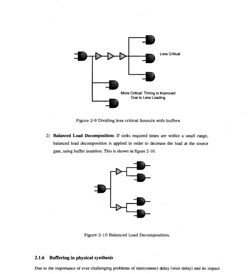
1) Critical Path Isolation: During logic synthesis, when one or several sinks (fanouts) are timing-critical, the critical path isolation technique generates a fanout tree so that the root gate drives the critical sinks while the non-critical sinks are separately driven by a buffer tree. In figure 2-9 an example of an optimized circuit with 3 buffers shows how the fanouts of a logic gate are divided into critical and non-critical parts such that non-critical fanouts can be driven with buffers.
....WHHIK.
—•!
Less Critical"El
More Critical: Timing Is improved Due to Less Loading
Figure 2-9 Dividing less critical fanouts with buffers
2) Balanced Load Decomposition: If sinks required times are within a small range, balanced load decomposition is applied in order to decrease the load at the source gate, using buffer insertion. This is shown in figure 2-10.
Figure 2-10 Balanced Load Decomposition.
2.1.6 Buffering in physical synthesis
Due to the importance of ever challenging problems of interconnect delay (wire delay) and its impact on physical design, first the interconnect delay problem and its potential solutions are discussed, and then the way that buffering can contribute to solving this problem is examined.
As feature size becomes smaller and chip area becomes larger in integrated circuits, the importance of interconnect delay increases rapidly with respect to gate delay. As a result, interconnect delay at the global level has become a critical factor in determining the system performance in deep submicron designs. Starting with the 0.25 um generation, circuit delay has been dominated by interconnect delay, as it is explicitly shown in figure 2-11.
-*- Gate Delay
-*- Sum of Delays, At SS(02
• • Sura of Delays, CM S Lows -*- Interconnect Delay, Al&SiOj
I - interconnect Delay, Cu $ Low <
M XQftii <m Cu 1.7 tid-cm Lews a~2.0
& Cut ,8/i Thkk & Cu Line 43 ulong
m m
350
m m m
w
Generation jrtm)
Figure 2-11 The dominance of interconnect delay.
Calculated gate and interconnect delay versus technology generation illustrating the dominance of interconnect delay as feature sizes approach 100 nm. [BOHR, 1995]
Vast efforts have been taken to control interconnect delay. There exist two main techniques:
Processing technology; New materials, such as copper and low dielectric constant (K) materials, have been used to improve interconnect performance. However, at the global interconnect level the benefit of material changes alone is insufficient to meet overall performance requirements. Even with the help of copper and low (K) materials, it is predicted that interconnect delay is still likely to dominate the chip performance beyond the lOOnm technology. Therefore, the significance of interconnect delay is expected to rapidly increase in the near future.
Design Technology: Using automated design tools and efficient algorithms, a permanent goal is to reduce circuit delay during the synthesis steps. Miscellaneous interconnect performance optimization techniques are done in synthesis procedures, like topology construction, buffer insertion, driver sizing, wire sizing and wire spacing. It has already been explained how and at which level buffering is done in logic synthesis. The methods that take buffering concerns into account during physical design are briefly reviewed, starting with an introduction to physical synthesis.
Having generated netlists during logic synthesis, physical synthesis performs the operations needed to produce the final circuit. The necessary steps to electrically implement the initial circuit design are as follows:
1) Partitioning: if too large to fit into one ASIC (Application Specific Integrated Circuit), functional blocks are split, or partitioned, into smaller blocks considering predefined design objectives. The product of this phase is then a netlist describing circuit blocks.
2) Floorplanning: having a hierarchical netlist that describes the interconnection of the blocks, floorplanning tools map this netlist into a physical description. The task of floorplanning ranges from arranging logic cells within the blocks to deciding about I/O pads and type of clock distribution.
3) Placement: At this level, logic cells are placed within flexible blocks. Since, after floorplanning and placement both intrablock and interblock capacitances are predictable, it is possible to return to the logic synthesis domain to re-optimize the design with more accurate estimates of the capacitive loads that each logic gate must drive.
4) Routing: The routing task consists of making connections between the blocks and within the designated channels defined by earlier phases.
5) Compaction: To minimize the overall circuit area, a set of optimization actions are performed to make the routed blocks as compact as possible.
6) Extraction and Verification: During the extraction step, the interconnection resistance and capacitance are determined and together with the entire design are sent for timing verification. At this step, the cost and design objectives along with the logical functionality are tested to ensure all design targets are met.
A summary of the physical synthesis steps is provided in figure 2-12.
KirMinnin.! I wpU«m.iq • r'-i' Placpnienl RcuLng Compaction t-*!i"ri'.:tcn and Venticotioi
Figure 2-12 Physical synthesis procedure [SMITH, 1998]
As mentioned before, buffering considerations are taken into account in physical synthesis. This is done at 3 different levels of physical synthesis [CONG and YUAN, 2000]:
1) Pre-routing (Placement and Floorplanning) stage: To obtain better routability, a number of methods consider some particular places for buffer insertion during the floorplanning step. This is helpful because during or after the routing step, most of the area is occupied by logic blocks and wires. Therefore ignoring buffer insertion during pre-routing steps can seriously restrict the space available for buffering.
2) Routing stage: In conventional design flows, fanout optimization and routing generation are often performed in a sequential manner, which means buffer insertion is used as a post-layout optimization technique after the routing stage. Consequently, a solution obtained during one of these optimizations becomes a constraint for the other one. Solving the unified problem, i.e. generating a buffered routing tree for a set of sinks and a driver, helps capturing the intrinsic interactions between the combined design steps and produces higher-quality implementations by systematically searching a much larger solution space.
3) Post-routing stage: Buffer insertion is typically a post-layout optimization technique, meaning that it is applied to improve the layout and delay after the routing stage. Having more realistic wire and load capacitance estimates at this level, the previously generated buffer tree is likely re-optimized to yield better circuit timing.
As devices shrink in size, the focus is being narrowed more and more on buffering in physical synthesis. In the next section, the major work done for buffer tree construction in both logic and physical synthesis will be briefly reviewed.
2.2 Previous Work
There are two main groups of buffer insertion techniques: Van Ginneken's method [VAN GINNEKEN, 1990] and its variations, and other methods which are not extensions of Van Ginneken's method. As many of the practical buffer insertion techniques in use today are based on the important work of Van Ginneken, this algorithm is studied first. Then other major efforts which basically extend Van Ginneken's method are examined. Buffer insertion methods that are not extensions of Van Ginneken's algorithm are discussed last. Different issues such as multi-type buffering, simultaneous routing and buffering, buffer sizing, continuous buffer insertion and buffered clock trees are addressed in this section which provides a good insight about the major challenges in this field.
2.2.1 Early efforts on optimal buffer insertion: Van Ginneken's algorithm
Van Ginneken proposed a dynamic programming algorithm [BELLMAN, 1957] for inserting buffers into a given topology. His algorithm returns the optimal solution in terms of Elmore delay [ELMORE, 1948], taking RC effects into account. For given required times at the sinks of the wiring tree, the algorithm chooses buffers such that the required time at the source is as late as possible. The topology of the wiring tree is assumed given, as well as the legal positions for the buffer insertion. The algorithm uses a depth first search on the wiring tree to construct a set of connected capacity-required time pairs (C, Q) that correspond to different choices for possible assignment of buffers. These pairs are inserted directly after branching points and at the legal positions. The structure of Van Ginneken's algorithm is shown in figure 2-13.
y^\. Legal yf Nw Buffering !'- '3 • / >». <r rvi S- Position
Figure 2-13 Van Ginneken's algorithm.
As the algortihm is based on dynamic programming, it consists of two main phases: bottom-up prediction and top-down decision making.
During the first phase the algorithm computes all options for each node. A set of (C, Q) pairs are constructed and stored. Then, for the options at the root of the tree delay, options are calculated and the option with the best source delay is chosen. The final solution is constructed during the second phase where the computations that led to the best option at the source are traced back. Buffers are placed during this phase.
According to Van Ginneken, in addition to timing optimization, the number of buffers can also be optimized. This is done by using triples of numbers rather than pairs for the options. Each option, in addition to the required time and the load, also has a solution cost. At the time of decision making, an option can only be discarded if it is worse in all three respects.
2.2.2 Extensions of Van Ginneken's algorithm
Despite its optimality under certain conditions, Van Ginneken's algorithm has some drawbacks as well. The time and space complexity of Van Ginneken's method is O (n2) [ALPERT et ai, 2000] [ZHOU et ai, 2000] where n is the number of buffer positions. Therefore, for large fanouts this method becomes inefficient. Besides, Van Ginneken' algorithm only works with a single-type of non-inverting buffers where only one legal buffering position is considered between two nodes. A number of techniques have consequently been proposed to efficiently enhance the complexity of the algorithm [SHI and zi, 2005] or to allow the algorithm to work with a buffer library consisting of inverting and non-inverting buffers with different physical characteristics [HRKIC and LILLIS, 2002] [Sffl and zi, 2005] [ALPERT et ai, 2000].
One can improve the time and memory complexity of Van Ginneken's by performing a set of modifications on the original algorithm. These modifications are based on finding and removing redundant solutions and are performed through 3 steps [SHI and zi, 2005]:
1) Predictive Pruning: Examining the options produced during the first phase of Van Ginneken's algorithm, one notices that some options are potentially dominated by some other options. In fact, whenever option A provides larger time slack and smaller input capacitance than option B, option A dominates option B, i.e. option B becomes a redundant solution. Speed-up is achieved by finding and pruning future redundant solutions.
2) Making Option Tree: Organizing the options information in an efficient data structure like a balanced binary tree helps achieving faster decision making process during the second phase of Van Ginneken's problem. Utilizing such a system also results in smaller memory consumption.
3) Fast Merging: Having one balanced binary tree for each option and its sub-tree information, the final solution is quickly constructed by merging those binary trees during the bottom-up phase.
Performing these techniques Van Ginneken's approach time complexity reduces to 0 (n log2 n) while
only O (n log n) memory is needed to construct the buffer tree.
To remove the drawback of single type buffering, some methods have been introduced to make it possible to do multiple buffer insertions. A primary solution quality improvement is achieved by taking b buffer types into account in the original Van Ginneken's algorithm. However, this basic
extension leads to 0(b2n2) runtime [HRKIC and LILLIS, 2002]. Better runtime is achievable if the 3 mentioned modifications consider a buffer library as well. This results in O (b2n log2(n)) runtime [SHI
and zi, 2005]. Modern design libraries may contain hundreds of different buffers, which may be either inverting Or non-inverting. If a user supplies every buffer available for the given technology as input to the buffer insertion tool, it could possibly take several days or even weeks to run to completion on a large design. Consequently, an appropriate set of buffers must be carefully selected to reduce the runtime [ALPERT et ai, 2000]. This is done in two steps. First, according to the physical characteristics of buffers a pruning process is applied to find the superior buffers and discard the rest. These superior buffers are chosen based on a performance criteria defined by the user, such as intrinsic delay, high noise margins, etc. This subset of superior buffers may be larger than the allowable buffer library size, again defined by the user. Therefore, during the second step, similar buffers are clustered and smaller buffer libraries are formed. A new size-reduced buffer library is created by choosing a number of smaller libraries. The metric used for proximity between buffers is their timing properties expressed as a linear delay function.
A different solution to multiple-buffer insertion is buffer sizing. Instead of a discrete buffer library, some methods allow for continuous buffer sizing [VOGEL and WONG, 2006] [CHEN et ai, 2002] [CHU and WONG,
1997]. As the input capacitance and the output resistance of the buffer can be expressed as the linear functions of the buffer size, different timing properties such as faster rise time or faster intrinsic delay are achieved by varying the transistor widths of the buffer. This removes the need, to have a buffer library and also helps meeting the timing requirements of the circuit, but at the cost of more computational efforts.
Van Ginneken's algorithm assumed only one buffer per wire in the tree. This assumption can severely hurt solution quality if the wire delay is taken into account. Instead, one can divide each wire into smaller segments, and hence introducing new legal buffering positions to insert buffers. Although segmenting each wire into small wires can help finding better buffering solutions, establishing the right number of wire segments is crucial. A small number of wire segments may result in sub-optimal solution, whereas a large number of wire segments may significantly increase CPU time. The ideal number of wire segments has been studied [ALPERT and DEVGAN, 1997] and the appropriate number of wire segments has been computed. This is done based on using only one buffer type. Handling a buffer library is achieved by obtaining the ideal wire segmenting factor for each buffer type, and choosing the maximum number of wire segments achieved for different buffers to guarantee the solution optimality [ALPERT et ai, 2000].
The extensions of Van Ginneken's algorithm mentioned above are done mainly during logic synthesis. However, some other extensions take buffer insertion into account during physical synthesis. These extensions are categorized in 2 groups:
1) Simultaneous routing and buffer tree construction (buffered routing)
In modern circuit fabrications chips becomes more congested, the number of metal layers used increases and interconnect delay dominates gate delay in establishing the overall circuit performance. Consequently, the important tradeoff between routing resource cost and signal delay is unavoidable. Some researchers consider simultaneous routing tree construction and buffer insertion to tackle this problem
[TANG and WONG, 2004] [OKAMOTO and CONG, 1996a] [LILLIS et al, 1996a] [SALEK et al, 1999] [CONG and YOUAN, 2000] [HRKIC and LILLIS, 2002], which is an NP-hard problem [SHI et al, 2004].
Early efforts on buffered routing started with combining routing techniques with Van Ginneken's algorithm in 1996. While a method [OKAMOTO and CONG, 1996b] was proposed to construct the fastest buffer tree based on the A-Tree routing topology
[CONG et al, 1993] , s o m e Other a p p r o a c h e s [LILLIS et al, 1996a] [OKAMOTO and CONG, 1996a] Were
proposed to use P-Tree routing topology [LILLIS et al, 1996b] during buffer insertion. In 1999, a more general buffered routing algorithm based on the P-Tree method was proposed [SALEK et al, 1999]. This method is called MERLIN. Introducing Ca-Tree as an extended version of P-Tree, MERLIN solves the buffered routing problem in polynomial time where multiple-buffer insertion is also allowed. A concept that MERLIN introduced for the first time was the 3-dimensional curves to take buffer location and area into account. These 3-dimensional curves consist of required time and load capacitance versus total buffer area. The third dimension (total buffer area) allows the user to solve the problem for either one of the following variants:
I) Minimizing the required time subject to an area constraint II) Minimizing the area subject to a required time constraint
2) Handling buffer insertion during floorplanning (pre-routing stage)
As the amount of communication among modules rapidly increases, it becomes more and more difficult to insert buffers to remedy interconnect during or after routing,
since most silicon and routing resources are already occupied. To that effect, some solutions have been proposed to consider buffering before routing and during the floorplanning stage by reserving particular areas for buffers [JIANG and CHANG, 2004] [KANG et ai, 1997a]. These reserved areas are known as buffer blocks. The Buffer Blocks are used to guarantee an effective interconnect optimization during the routing stage. The designated regions for buffer insertion may significantly change the floorplan and placement, thus causing problems in timing closure and design convergence. It is possible to do buffer block planning during the floorplanning stage [JIANG and CHANG,
2004], or construct a bounded delay tree, and then use Van Ginneken's algorithm to optimize buffers [KANG et ai, 1997a].
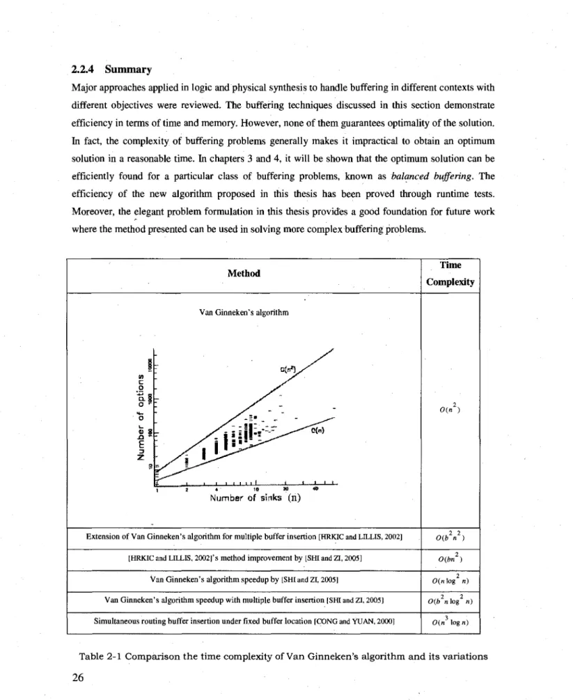
A summary of the time complexity of Van Ginneken's approach and some of its variations is shown in table 2-1 (at the end of the chapter). In this table n represents the number of sinks and b represents the number of buffers available in the buffer library.
2.2.3 Other Work
Due to the importance and wide applications of buffered routing, numerous methods have been proposed that are not extensions of Van Ginneken's algorithm. Many of these methods are graph-based and are known as maze routing approaches [LAI and WONG, 2000] [ZHOU et ai, 2000] [HUANG et ai, 2003]. The goal of maze routing is to find a route between two terminals in a routing area, which is often represented as a grid graph. Some wiring obstacles and restrictions on buffer locations and types may be present in the routing area. One major advantage of maze routing approaches over the extensions of Van Ginneken's algorithm is that they are formulated as shortest path problems. Therefore, efficient software routines solving shortest path problems in existing graph application libraries can be used in buffered routing. A sample routing grid graph and a buffered minimum delay path is shown in figure 2-14 [LAI and WONG, 2000]. The dark areas represent wiring obstacles. Buffers can not be placed in gray and dark regions, while wires are allowed to pass through gray areas. Solid circles at some of the grid line intersections are possible buffer locations or previously mentioned legal positions.
Figure 2-14 A routing grid graph and a buffered minimum Elmore delay path.
For a buffer insertion technique to be effective, it must be fully aware of its surrounding blockage constraints. During the routing process, there are macro-blocks placed within the area. These blocks form useful routing regions because wires are allowed to run over them, whereas buffers are not allowed to use them, since in that case the design of those blocks has to be changed. One brute force solution is to ignore macro blocks during routing. In this way, first a shortest path is found and then buffers are inserted outside the macro blocks. If there is no macro block, it can be proved that this sequential two-stage routing and buffer insertion approach gives an optimal solution. However, with macro blocks, a shortest path no longer guarantees minimum delay. The fast path algorithm [ZHOUetai, 2000] is a way of simultaneously doing routing and buffer insertion with blockage avoidance. This method extends Dijkstra's shortest path algorithm to do a general labeling, based on the Elmore delay model where path length is substituted by Elmore delay in Dijkstra's algorithm. Unlike Dijkstra's algorithm, the sub-path of a shortest path in this solution is not necessarily a shortest one. The total runtime of the fast path algorithm is 0(nv(e+nv) log(nv)), where n represents the number of possible buffer positions, v is the number of vertices and e is the number of edges. A similar work that also considers wire sizing has a 0(v2 log(v)) runtime and 0(b2v2) space complexity where v is the vertices
in the grid graph and b is the number of buffers available in the buffer library [LAI and WONG, 2000]. In buffered routing more accurate delay models can also be used (transmission lines, delay look-up tables, etc.) [HUANG et ai, 2003J. In this method, only those vertices which have qualifying transition time are included in the graph. This technique guarantees that all transition time constraints are satisfied. With k transition time bins and v vertices in the grid graph, the time and space complexity of this method is O(kV).
In addition to maze routing algorithms, some studies have been done on different tradeoffs in buffered routing. As a result of the intrinsic complexity of buffered routing, one has to carefully deal with various design parameters where each design objective becomes a constraint for the other ones. Based on a previously proposed buffered routing method [TANG et ai, 2001], [TANG and WONG, 2004] widely discusses different approaches to tackle the tradeoff between signal delay and routing cost by formulating the problem as a linear function of all design constraints.
As opposed to the buffering methods reviewed so far, a number of approaches assume no restriction for buffer positions and buffer sizes. These methods are known as continuous methods. For buffer insertion on a single line allowing continuous buffer positions and continuous buffer sizes, Dhar and Franklin [DHAR and FRANKLING, 1991] proposed a closed form solution, and Chu and Wong [CHU and WONG,
1999] proposed a quadratic programming approach. However, it should be pointed out that as opposed to the discrete version of the buffer insertion problem, the continuous methods can not be applied to trees. This drawback limits the applications of such approaches.
The minimization of total wire length is of interest since total wire length contributes to circuit area and routing congestion. As a result, some methods have been proposed to optimize total wire length as primary objective, with satisfying delay bounds as secondary objective [ZHU, 1995] [RANG et ai, 1997b]. These methods are basically known as delay bounded algorithms. Delay bounded minimum Steiner tree or DBMST is one way to construct a low cost Steiner tree with bounded delay at critical sinks [ZHU, 1995]. The DBMST algorithm consists of two phases:
(1) Initialization of Steiner tree subject to timing constraints
(2) Iterative refinement of the topology to reduce the wiring length while satisfying the delay bounds associated with critical sinks.
Since the Elmore delays at sinks are very sensitive to topology and they have to be recomputed every time the topology is changed, the DBMST algorithm searches all possible topological updates exhaustively at each iteration and as a result is very time consuming. The delay bounded minimum buffered tree or DBMB-tree algorithm as an extension of DBMST has smaller time complexity 0(n2)
where n is the total numbers of the terminals of the net [KANG et ai, 1997b]. This algorithm successfully combines the local stochastic hill climbing features from SA (Simulated Annealing) and the global crossover operation from GA (Genetic Algorithm) in an optimization method, named genetic simulated annealing (GSA). Also, a multi-dimensional acceptance function is defined to accept the candidate solutions along the single search path generated by SA-based local moves. This multi-24
dimensional function is defined based on the votes of the experts, and the objectives are ordered by sensitivity defined for each of them.
More accurate delay models have been investigated by some researchers. While RC (Resistance-Capacitance) models are used for high resistance nets, inductance is becoming more important with faster on-chip rise times and longer wire lengths. Wide wires are frequently encountered in clock distribution networks and in upper metal layers. These wires have low resistance and can exhibit significant inductive effects. Furthermore, performance requirements are pushing the introduction of new materials for low resistivity interconnects. Inductance is therefore becoming an essential element in VLSI design methodologies. The Elmore delay does not consider non-monotonic responses which can occur in RLC (Resistance-Inductance-Capacitance) circuits. Therefore, some approaches have been proposed to take wire inductance into account. For example, one method introduces a simple tractable delay formula for RLC trees that preserves the useful characteristics of the Elmore delay model [ISMAIL et ai, 1999]. In this method the rise time of the signals in an RLC tree is characterized as well as the overshoots and the settling time.
Clock tree buffering is also addressed by a number of methods [WANG et ai, 2005] [TELLEZ and
SARRAFZADEH, 1997] [ALPERT et ai, 200i]. In high performance synchronous VLSI design, system performance is limited by the quality of its clock signal, which is measured by the clock skew, clock slew and clock phase delay. The clock skew is defined as the maximum difference between the arrival times of the signals at all of the clock sinks. The clock slew is the slope of clock signals and the clock phase delay is defined as the maximum delay from the clock source to any clock sink [WANG et ai, 2005]. Without a careful design, clock skews can cause lower clock frequency (zero clocking) as well as race conditions that result in failure regardless of frequency (double clocking). These two important factors can be optimized by good routing strategy and effective buffer insertion. The most common clock distribution network is a buffered tree. The focus of buffered clock tree systems usually is on skew minimization whereas a good buffer tree can also improve slew rate. Since bounding the load capacitance is a well known method to improve coupling noise immunity most of the buffered clock-tree algorithms use bounded load capacitances to guarantee meeting the electrical constraints [TELLEZ
and SARRAFZADEH, 1997] [ALPERT et ai, 2001]. However, one major drawback of such algorithms is that they
2.2.4 Summary
Major approaches applied in logic and physical synthesis to handle buffering in different contexts with different objectives were reviewed. The buffering techniques discussed in this section demonstrate efficiency in terms of time and memory. However, none of them guarantees optimality of the solution. In fact, the complexity of buffering problems generally makes it impractical to obtain an optimum solution in a reasonable time. In chapters 3 and 4, it will be shown that the optimum solution can be efficiently found for a particular class of buffering problems, known as balanced buffering. The efficiency of the new algorithm proposed in this thesis has been proved through runtime tests. Moreover, the elegant problem formulation in this thesis provides a good foundation for future work where the method presented can be used in solving more complex buffering problems.
Method Numbe r o f option s SO 10 0 190 9 1000 0
Van Ginneken's algorithm
/ s nil:-"—
j--^oW
y^ i L.—
1 J 4 10 » «
Number of sinks (n)
Extension of Van Ginneken's algorithm for multiple buffer insertion [HRKIC and LILLIS, 2002]
[HRKIC and LILLIS, 2002]'s method improvement by [SHI and ZI, 2005]
Van Ginneken's algorithm speedup by [SHI and ZI, 2005]
Van Ginneken's algorithm speedup with multiple buffer insertion [SHI and ZI, 2005]
Simultaneous routing buffer insertion under fixed buffer location [CONG and YUAN, 2000]
Time Complexity 0(n) 2 2 0(b n ) 0(bn2) 2 0(n log n) 2 2 0(b nlog n) 3 0(n log «)
Table 2-1 Comparison the time complexity of Van Ginneken's algorithm and its variations 26
Chapter 3
• BALANCED B U F F E R I N G
In this chapter a specific buffering problem is addressed and a new solution is proposed. The objective of the buffering method introduced is to generate the fastest buffer tree for a set of identical fanouts,(identical in terms of capacitance and required time). Due to the symmetrical buffer tree structure obtained by the proposed method, it is called balanced buffer tree while the process of producing a balanced buffer tree is known as balanced buffering. Analyzing this type of buffering from a mathematical point of view and extracting elegant formulas expressing the characteristics of the best buffer tree, a new buffering algorithm is proposed in this chapter1. The presented algorithm
ensures solution optimality due to the nature of the applied method which is branch-and-bound. While the tests provided in this chapter show a reasonable time and space complexity for the presented balanced buffering algorithm, a number of techniques will be introduced in chapter 4 to improve the performance of this algorithm. This chapter also encompasses some exclusively tailored data structure to the proposed problem-solving method. To strengthen the purpose of using an idea or a technique, adequate mathematical proofs are provided in appendices.
Chapter Outline
In section 3.1, the balanced buffering problem is discussed and its major characteristics are studied. Section 3.2 gives a formal definition of the balanced buffering problem. Section 3.3 examines the required conditions of using the branch-and-bound method to design the buffering algorithm and the structure of the feasible region (search space) explored by the buffering algorithm is examined. Section 3.4 presents the flowchart of the balanced buffering algorithm. In section 3.5, it is explained how solutions are handled by the algorithm. Section 3.6 studies the topology of balanced buffer trees and the proper ways of making balanced sub-trees to implement the branch-and-bound algorithm. In section 3.7 two rules are introduced to help avoiding non-promising solutions. Section 3.8 presents efficient techniques utilized to produce a neutral-phase buffer tree with a buffer library containing both inverting and non-inverting buffers. Finally, section 3.9 shows the runtime of the proposed buffering algorithm.
3.1 Balanced Buffering Applications: Facts and Potentials
As mentioned before, buffering is used at both logical and physical design levels to improve circuit timing and help decoupling large fanouts. In a typical buffering problem, the load specifications are not necessarily identical, i.e. the required times in logic synthesis and the realistic load capacitances obtained in physical design are regularly very diverse. However, certain types of circuitry do exhibit local specifications where loads have similar input capacitance and required time. This is the case where a balanced buffer tree is generated. In figure 3.1 two types of buffering problems are compared. Each box represents a load and the size of the box represents the load capacitance. In addition, the distance between the boxes and the source gate is used to depict their required times. The closer a box is to the source gate, the smaller its required time.
; \ R®q*j iredTi rtre Load Capacitance
—--•
"**>*" LoadA typicai buffering problem with different required times
arid load capacitances
•
D
D
•
Required Time
A balanced buffering problem with Identical required times
and load capacitances
Figure 3-1 Balanced buffering versus a typical buffering problem.
A good example of balanced buffer trees is in clock tree construction. The purpose of a clock signal in a synchronous digital design is to define a reference for data movement. Hence, the stability of clock signals is extremely important. One solution to distribute signals with minimal skews and healthy signal waveforms is to generate a tree with an H-form structure where the distances from the center to all branch points are the same, and hence, the signal delays would be the same. Typically, such a clock network should be a balanced buffer tree. Note that due to routing constraints and different fanout requirements, this is difficult to implement in practice, but certain methods have some preferences on
timing objectives rather than routing targets, and therefore, they use H-form clock trees as a pre-routing operation. H-form structure and a balanced buffer clock tree are shown in figure 3-2.
M
l L Ii—1>
I I I | I I
a) H-form structure for a clock tree
i—£>—a •—{>—a
i>
»-£> mf>—a
I h>.
b) Balanced buffer clock tree
Figure 3-2 Clock tree construction
Yet, this is not the only application for which this thesis proposes a buffering method. The long term goal of this work is for a designer to be able to solve even unbalanced buffering problems for more general cases by casting them into the balanced buffering model. However, in this thesis only balanced buffering problem is solved, the generalized techniques being left for future work.
Modeling of the problem is an important step toward solving it. If available, a mathematical model which can capture the basic characteristics of the problem is preferred because it can significantly simplify both developing and implementing the solution. In order to extract a mathematical model for the balance buffering problem it is therefore useful to find the minimum delay achievable for a typical buffering using a balanced buffer tree. More precisely, answering the following question leads to an elegant mathematical model:
Given a source and a set of identical loads with similar required time and capacitance, what is the best delay achievable by an ideal buffer treel
The term ideal buffer tree means a buffer tree which exhibits prefect timing properties but is not necessarily implementable. While in a typical tree branching factors and the depth of the tree are expressed by integer values, in an ideal buffer tree these parameters may be non-integer and hence make it impossible to implement such a tree. In this dissertation, the term ideal buffer tree will be used as opposed to real buffer tree which is an implementable tree. Also, Ideal delay and real delay will be used throughout this dissertation to indicate the delay values for each of the mentioned buffer tree
types. For more clarity, a statement of the problem follows, to determine the overall constraints and objectives with which the problem is going to be solved.
3.2 Statement of the Problem
The goal is to maximize the slack of the circuit, or simply minimize its delay. The physical properties of the source gate and its fanouts are given, and all fanouts are identical in terms of required times and physical characteristics. No routing topology is given and it is possible to freely look for the best buffer tree topology meeting the timing needs. It is preferred to use a buffer library consisting of inverting and non-inverting buffers to help finding better solutions to the problem. No buffer sizing is applied to reduce the circuit delay. The generated buffer tree must have a positive phase, i.e. in the presence of inverters no phase shifting is allowed to occur and the buffer tree must have no effect on the circuit logic. Thus, the problem is simply stated as:
Minimize Dft
Where Dyy denotes the overall delay of a network consisting of a source and its fanouts.
3.3 Method
Since the significant work of Van Ginneken [VAN GINNEKEN, 1990] which proposed a dynamic programming algorithm for inserting buffers and the work of Touati [TOUATI, 1990], many of the practical buffer insertion techniques in use today have been proposed to extend these algorithms or improve their time complexities. However, even though general buffering has been proven to be an NP-complete problem [BERMAN et ai, 1989] [SHI et ai, 2004], exhaustive search techniques, such as branch-and-bound algorithm, are more effective than dynamic programming in solving balanced buffering problems, due to the nature of such problems which exhibits good branching and bounding properties. In fact, searching for the best topology as well as the best buffer arrangement makes balanced buffering extremely difficult to solve with a dynamic programming technique. This is due to the fact that the efficient structure required to cast a balanced buffering problem into a dynamic programming pattern is hard to find as the best buffering configuration varies with topology changes. Therefore, a branch-and-bound method is chosen to cover all possible solutions to a balanced buffering problem. The branch-and-bound method was first introduced in 1960's in the Operations Research community
[LAND and DOIG i960]. It is discussed extensively in [MICHALEWICZ and FOGEL 2000] [AHO et ai, 1983] and only