UNIVERSITÉ DE MONTRÉAL
TRI-BAND CMOS CIRCUIT DEDICATED FOR AMBIENT RF ENERGY HARVESTING
YIQIU WANG
DÉPARTEMENT DE GÉNIE ÉLECTRIQUE ÉCOLE POLYTECHNIQUE DE MONTRÉAL
MÉMOIRE PRÉSENTE EN VUE DE L’OBTENTION DU DIPLÔME DE MAÎTRISE ÈS SCIENCES APPLIQUÉES
(GÉNIE ÉLECTRIQUE) FÉVRIER 2015
UNIVERSITÉ DE MONTRÉAL
ÉCOLE POLYTECHNIQUE DE MONTRÉAL
Ce mémoire intitulé :
TRI-BAND CMOS CIRCUIT DEDICATED FOR AMBIENT RF ENERGY HARVESTING
présenté par : WANG Yiqiu
en vue de l’obtention du diplôme de : Maîtrise ès sciences appliquées a été dûment accepté par le jury d’examen constitué de :
M. AUDET Yves, Ph. D., président
M. SAWAN Mohamad, Ph. D., membre et directeur de recherche M. KARIMI Houshang, Ph. D., membre
DEDICATION
ACKNOWLEDGMENT
My thanks are due, first and foremost, to my supervisor, Professor Mohamad Sawan, for his patient guidance and support during my Master at Polytechnique Montréal. His many years of design experience in analog integrated circuit have allowed me to focus on a very promising and interesting project.
On the second place, I would like to thank my parents, who offered me their unconditional love and support, and encouraged me throughout my study.
My thanks go to my friendly colleagues for their friendship and for the pleasant atmosphere in the office they made, especially to thank Yushan Zheng for his help and friendship from the beginning of my Master, Seyed Saeid Hashemi for his useful instructions on rectifier design, Faycal Mounaim for his useful suggestions on rectifier measurement, Sami Hached and Mohamed Zgaren for their help on my French and their daily jokes, Bahareh Ghane-Motlagh for helping me cut the chip. Also I would like to thank my friends from PolyGrames: Kuangda Wang for his help on rectifier measurement and Ajay-Babu Guntupalliu for his advice on antenna design.
Last but not least, I would like to thank Marie-Yannick Laplante for her responsibility, Laurent Mouden for his wire bonding and Réjean Lepage for his software support.
RÉSUMÉ
L'utilisation de systèmes sans fil connait une croissance rapide dans divers domaines tels que les réseaux de téléphonie cellulaire, Wi-Fi, Wi-Max, la radiodiffusion et les communications par satellite. Cette croissance mènera à une quantité considérable d'énergie électromagnétique générée dans l'air ambiant, mais toujours en dessous des limites de sécurité internationales. Ainsi, la recherche au niveau des systèmes de récupération d'énergie RF pour alimenter des appareils électroniques miniaturisés à faible consommation de puissance devient attrayante et prometteuse.
Le bloc principal dans un système de récupération d'énergie RF est le redresseur qui détermine l'efficacité et la sensibilité de l'ensemble du système. Étant donné que la puissance RF ambiante est très faible, la quantité d'énergie captée par l'antenne l’est également. En outre, il y a des pertes au niveau du réseau d'adaptation d’impédance qui réduisent encore plus la puissance transmise au bloc redresseur. Par conséquent, la puissance disponible est trop faible pour faire fonctionner des redresseurs classiques.
Dans ce mémoire, nous proposons trois redresseurs à trois-étages et à grilles totalement croisées-couplées en utilisant des transistors à faible tension de seuil afin d’opérer à de faibles puissances d'entrée. Les trois redresseurs ont été conçus et intégrés au sein d’une même puce fabriquée en utilisant une technologie CMOS 130nm d’IBM. Ils ont été optimisés à des fréquences de 880MHz, 1960MHz et 2.45GHz respectivement. Les résultats expérimentaux démontrent qu’ils atteignent une efficacité de conversion de puissance maximale de 62%, 62% et 56.2% respectivement. Les mesures montrent également une grande amélioration de l'efficacité à de faibles niveaux de puissance d'entrée. Afin de récupérer l'énergie ambiante de trois principales sources RF au Canada – GSM-850, GSM-1900 et Wi-Fi, un système de redresseur utilisé pour la combinaison de la puissance de ces trois canaux est simulé et analysé. Le système utilise une topologie consistant simplement à connecter les sorties des redresseurs ensemble pour charger le condensateur de charge. En dépit de la grande amélioration de l'efficacité et de la sensibilité dans la plage de 0-5μW, une baisse d'efficacité indésirable se produit aux puissances plus élevées. Ainsi, un nouveau bloc de gestion de l'alimentation est proposé. De plus, une antenne tri-bande est conçue et simulée pour diminuer le volume de l'ensemble du système de récupération d'énergie RF. En particulier, les pertes par réflexion obtenues sont de -25.43dB, -13.92dB et -12.73dB aux fréquences citées plus haut respectivement.
ABSTRACT
Nowadays, the use of wireless systems has grown rapidly in various domains such as cellular phone networks, Wi-Fi, Wi-Max, radio broadcasting and satellite communications. The growing use of these wireless systems leads to considerable amount of electromagnetic energy generated in ambient air (of course, still below international safety limits). Thus the research in ambient RF energy harvesting system dedicated for powering up low-power-consumption miniaturized electronic devices becomes attractive and promising.
The main block in a RF harvesting system is the rectifier which determines the efficiency and sensitivity of the whole system. Since ambient RF power is very low, the amount of power captured by the antenna is extremely low. Besides, there is loss on matching networks, thus the available power given to the rectifier block is too low for traditional rectifiers to operate. Therefore, in this master thesis, three three-stage fully gate cross-coupled rectifiers using low-threshold-voltage transistors are proposed to overcome the dead zone in low input power range. The three rectifiers optimized at 880MHz, 1960MHz and 2.45GHz frequencies respectively are designed on one chip layout. Their experimental results are retrieved from this custom fabricated integrated circuit using IBM 130nm CMOS technology. They achieve peak efficiencies of 62%, 62% and 56.2% respectively and show great improvements on power conversion efficiency at low input power level.
In order to harvest ambient RF energy from the three main RF contributors in Canada – GSM-850, GSM-1900 and Wi-Fi 2.4GHz, a rectifier system used for power combination from these three channels is simulated and analyzed. The system employs a simple topology by connecting the outputs together to charge the load capacitor. In spite of its high improvements on efficiency and sensitivity in 0-5μW range, an undesirable efficiency drop happens at higher input power levels. Thus an idea of power management block is proposed.
In addition, a tri-band antenna is designed and simulated so as to decrease the volume of the overall RF energy harvesting system. It achieves return loss of 25.43dB, 13.92dB and -12.73dB at each desired band respectively.
TABLE OF CONTENTS
DEDICATION ... III ACKNOWLEDGMENT ... IV RÉSUMÉ ... V ABSTRACT ... VI TABLE OF CONTENTS ... VII LIST OF TABLES ... X LIST OF FIGURES ... XI LIST OF ABBREVIATIONS AND SYMBOLS ... XIV LIST OF APPENDIXES ... XVI
CHAPTER 1 INTRODUCTION ... 1
1.1 Background ... 1
1.2 Objectives ... 2
1.3 Thesis organization ... 2
CHAPTER 2 LITERATURE REVIEW ... 4
2.1 Energy harvesting ... 4
2.2 RF energy harvesting (RF-EH) ... 6
2.3 Ambient RF energy ... 9
2.4 Rectifier ... 10
CHAPTER 3 RECTIFIER DESIGN AND POST-LAYOUT SIMULATION ... 14
3.1 Overview of rectifiers: popular CMOS rectifier structures ... 14
3.1.1 Basic structures of MOS-based rectifier ... 15
3.1.2 Advanced bridge MOS-based rectifiers ... 17
3.2.1 Attempt to improve the work proposed by Hashemi et al. (2012) ... 20
3.2.2 Analysis of single-stage FGCC rectifier ... 22
3.2.3 Necessity of cascading stages of the FGCC rectifier ... 24
3.2.4 PCE comparison of 3-stage FGCC rectifiers using various transistors ... 26
3.2.5 PCE comparison of 3-stage FGCC rectifiers using different bulk connections ... 27
3.2.6 Design of 3-stage FGCC rectifier ... 28
3.2.7 Layout design ... 28
3.3 Post-layout simulation results of the designed 3-stage FGCC rectifier ... 30
3.3.1 Vout simulation ... 30
3.3.2 PCE simulation ... 31
CHAPTER 4 SYSTEM IMPLEMENTATION AND POST-LAYOUT SIMULATION ... 33
4.1 General concept of multi-channel power combination ... 33
4.2 Post-layout simulation results of multi-channel rectifier ... 35
4.3 Reason of the efficiency drop at higher power levels ... 37
4.4 Strategy for preventing reverse leakage ... 38
4.4.1 General concept of micropower management ... 38
4.4.2 Proposed strategy for power management ... 39
CHAPTER 5 MEASUREMENT OF RECTIFIER ... 42
5.1 Measurement Setup ... 42
5.1.1 PCB design ... 42
5.1.2 Equipments and calibration ... 45
5.2 Measurement results ... 47
5.2.1 Process of data ... 48
CHAPTER 6 TRI-BAND ANTENNA DESIGN ... 57
6.1 RF power transmission ... 57
6.2 Microstrip patch antenna ... 58
6.2.1 General characteristics ... 58
6.2.2 General advantages of MPA ... 59
6.3 Designed tri-band microstrip patch antenna ... 60
CHAPTER 7 GENERAL DISCUSSION: RECTIFIER COMPARISON WITH PREVIOUS WORKS ...64
CONCLUSION ... 66
LIST OF TABLES
Table 2.1: The typical autonomy of several battery-powered electronic devices, from Vullers et al.
(2009) ... 4
Table 2.2: Comparison of published works (* calculated from graph) ... 7
Table 2.3: Comparison of published works (* calculated from graph) (continued) ... 8
LIST OF FIGURES
Figure 1.1. General diagram blocks for RF-EH ... 2
Figure 2.1 DBS on diode-connected transistors, from Ahmadi et al. (2005) ... 10
Figure 2.2 (a) DBS and parallel diodes, from Ghovanloo and Najafi (2004). (b) DBS and bootstrapped capacitors, from Hashemi et al. (2012). ... 12
Figure 2.3 Improved FGCC, from Theilmann et al. (2010) ... 12
Figure 2.4 (a) DBS technique from Wang et al. (2007). (b) Floating-gate technique from Le et al. (2008). ... 13
Figure 3.1 Conventional MOS-based half-wave rectifier ... 16
Figure 3.2 Waveforms of the conventional MOS-based half-wave rectifier from Yi et al. (2007): (a) Waveforms of input and output voltages, (b) Waveforms of transistor current. ... 16
Figure 3.3 Conventional MOS-based full-wave bridge rectifier (nMOS transistors are used) ... 17
Figure 3.4 Partially gate cross-coupled rectifier (nMOS transistors are used) ... 18
Figure 3.5 Fully gate cross-coupled rectifier ... 19
Figure 3.6 Charge-Pump based rectifier ... 20
Figure 3.7 PCE of the rebuilt rectifier of Hashemi et al. (2012) and comparison with those of fully and partially gate cross-coupled structures ... 21
Figure 3.8 Operation of P1 and N2 of single-stage FGCC CMOS rectifier: (a) Conduction on linear mode (point A in Figure 3.9), (b) Conduction on subthreshold mode (point B in Figure 3.9). ... 22
Figure 3.9 Theoretical analysis of single-stage FGCC rectifier ... 23
Figure 3.10 Proposed three-stage FGCC rectifier ... 25
Figure 3.11 PCE comparison of 3-stage FGCC rectifiers using LTV and STV transistors ... 26
Figure 3.12 PI triple well LTV nMOS transistor: (a) Cross section view from IBM Training file, (b) Symbol view. ... 27
Figure 3.13 PCE comparison of 3-stage FGCC rectifier structure using different bulk connection
... 28
Figure 3.14 Layout of transistors: (a) nMOS LTV, (b) pMOS LTV. ... 29
Figure 3.15 Vout vs. input power of the designed rectifier with different loads ... 31
Figure 3.16 PCE vs. input power of the designed rectifier with different loads ... 32
Figure 4.1 Simplified block diagram of tri-channel rectifier system dedicated for EH from three RF bands, Wang and Sawan (2014). ... 34
Figure 4.2 Comparison of PCE of rectifiers with different numbers of channels ... 36
Figure 4.3 Comparison of Vout of rectifiers with different numbers of channels ... 37
Figure 4.4 Theoretical analysis of the efficiency drop ... 38
Figure 4.5 Proposed RF energy harvesting system with power management ... 40
Figure 4.6 Transient simulation results of the proposed rectifier system with power management: (a) when Pin2 >Pin3, (b) when Pin2 <Pin3. ... 41
Figure 5.1 Five main pads shown in schematic view ... 43
Figure 5.2 Photomicrograph of fabricated rectifier with its five main pads with wire bonding .... 43
Figure 5.3 Simplified layout view of the connections of the main five pads (not scaled) ... 44
Figure 5.4 Layout view of the designed PCB in ADS ... 44
Figure 5.5 PCB for chip testing ... 45
Figure 5.6 Calibration: (a) Power meter self calibration, (b) PNA source calibration, ... 46
Figure 5.7 Purpose of port extension ... 46
Figure 5.8 Design of an open to the portion of fixture ... 47
Figure 5.9 Model of s4p block in ADS for processing data ... 48
Figure 5.10 Measured PCE as a function of input power at 880MHz with 100kΩ, 50kΩ and 10kΩ load resistor ... 49
Figure 5.11 Measured PCE as a function of input power at 1960MHz with 100kΩ, 50kΩ and 10kΩ
load resistor ... 50
Figure 5.12 Measured PCE as a function of input power at 2.45GHz with 100kΩ, 50kΩ and 10kΩ load resistor ... 51
Figure 5.13 Measured PCE vs. Simulated PCE as a function of input power at 880MHz with 100kΩ load resistor and 60pF load capacitor ... 52
Figure 5.14 Measured Vout as a function of input power at 880MHz with 100kΩ, 50kΩ and 10kΩ load resistor ... 53
Figure 5.15 Measured Vout as a function of input power at 1960MHz with 50kΩ, 100kΩ and 200kΩ load resistor ... 54
Figure 5.16 Measured Vout as a function of input power at 2.45GHz with 50kΩ, 100kΩ and 200kΩ load resistor ... 54
Figure 5.17 Measured real part of Zin as a function of input power of the rectifiers dedicated for 880MHz, 1960MHz and 2.45GHz respectively ... 55
Figure 5.18 Measured imaginary part of Zin as a function of input power of the rectifiers dedicated for 880MHz, 1960MHz and 2.45GHz respectively ... 56
Figure 6.1 Illustration of power transmission from base station to harvesting devices ... 58
Figure 6.2 Cross section of a MPA in its basic form ... 59
Figure 6.3 Proposed volume-reduced RF harvesting system ... 60
Figure 6.4 Geometry of the designed tri-band MPA (dimensions in millimeter) ... 61
Figure 6.5 Simulated return loss of the designed antenna ... 62
Figure 6.6 Simulated 3D radiation pattern of the designed antenna: (a) at 880MHz, (b) at 1960MHz, (c) 2.45GHz ... 63
Figure 7.1 Comparison with published works (PCE as a function of input power) ... 64
LIST OF ABBREVIATIONS AND SYMBOLS
AC: Alternative Current
ADE: Analog Design Environment BEH: Biological Energy Harvesting DC: Direct Current
DBS: Dynamic Bulk Switching DRC: Design Rule Check EH: Energy Harvesting
FGCC: Fully Gate Cross-Coupled GND: GROUND
GSM: Global System for Mobile Communications HFSS: High Frequency Structure Simulator LIP: Low Input Power
LTV: Low-Threshold-Voltage LVS: Layout Versus Schematic MOS: Metal-Oxide-Semiconductor MPA: Microstrip Patch Antenna
nMOS: n-type Metal-Oxide-Semiconductor PCB: Printed Circuit Board
PCE: Power Conversion Efficiency PGCC: Partially Gate Cross-Coupled pMOS: p-type Metal-Oxide-Semiconductor RF-EH: RF Energy Harvesting
SEH: Solar Energy Harvesting STV: Standard-Threshold-Voltage TE: Thermoelectric
VDD: label of input power
LIST OF APPENDIXES
APPENDIX A– MA LAST METAL CROSS SECTION ………76 APPENDIX B– SCHEMATIC VIEW OF THE DESIGNED 3-STAGE FGCC RECTIFIER …77 APPENDIX C– LAYOUT OF THE DESIGNED 3-STAGE FGCC RECTIFIER ………..78 APPENDIX D– SCHEMATIC VIEW OF THE COMPARATOR AND INVERTER …………79
CHAPTER 1
INTRODUCTION
1.1 Background
Energy harvesting or power harvesting or energy scavenging is an approach to collect energy from external sources. One of the most popular energy harvesting (EH) method nowadays is radio-frequency (RF) EH (RF-EH), which seems to be initiated by radio-frequency identification (RFID) applications.
The existing applications of RF-EH are RFID (Shameli et al. (2007)), wireless sensor networks (Nishimoto et al. (2010)), RF-powered devices (Ouda et al. (2013)) and ambient-RF-powered devices (Li et al. (2013)).
Some modern medical devices (Ho et al. (2014)) tend to be RF-powered instead of battery-powered. This is mainly because the RF-powered medical devices can reduce the chances of infection and chemical instability, especially when the devices are implantable. RF-powered implants can prevent the patients from undergoing repeated surgeries to replace the out-of-power old device at intervals of several years. Furthermore, the battery size is always too large compared with the chip’s physical size. With the maturity of RF-EH technique, researchers can miniaturize the last thing that makes medical devices so large. However, so far, all reported RF-powered medical devices need a dedicated and specified RF source to supply enough RF power for the RF harvesting module of the biomedical device at a designated frequency and power density, which means that the patients need to carry a RF source at hand or keep staying near the RF source to make their implants work. Authors Visser and Vullers (2013) consider it as “RF energy transport” instead of “RF energy harvesting”.
In order to make the devices totally portable, ambient-RF-powered technique draws great attention of designers. Ambient RF-EH is the process where electromagnetic waves in the surrounding air, due to the growing presence of cellular phones and corresponding local area networks, are harvested and collected. However, not all RF–powered devices (near-field RF or far-field RF) can be turned to ambient-RF-powered ones. This is because the available/existing RF energy in the free air is limited and very low, thus only extremely low-power-consumption (only several microwatts) miniaturized electronic devices can be powered by ambient RF.
Figure 1.1. General diagram blocks for RF-EH
A RF-EH system needs an antenna for sensing electromagnetic waves and a rectifier for converting the sensed AC power to DC power. The DC power can then be used to power up an ultra-low-power system. Figure 1.1 shows the building blocks of a RF energy harvester, encompassing an antenna, an impedance matching network, a rectifier and a DC/DC up converter. Commonly multi-stage rectifier can be used to increase the rectified DC voltage instead of using an additional DC/DC up converter. Far-field RF energy transmission is concerned in this case, which is different from the near-field resonant inductive coupling and magnetic resonance coupling. Normally the power conversion efficiency (PCE) of the harvesting system is defined as the ratio of the load DC power to the available RF power at the antenna.
1.2 Objectives
In this Master work, the main objective is to develop a high-efficiency CMOS rectifier dedicated to recover energy from ambient RF through GSM-850, GSM-1900 and Wi-Fi 2.4GHz bands in the surrounding air.
In addition, multi-band rectifier system should be studied for the purpose of multi-band ambient RF-EH. In the meanwhile, a power management block should be proposed if needed.
1.3 Thesis organization
This master thesis contains seven chapters. Chapter 1, this chapter, introduces the background and the objectives of this Master work. Chapter 2 provides the literature review on topics: EH, RF-EH, feasibility of harvesting ambient RF energy and rectifier design. At the same time, main design challenges and optimizations on basic circuit structures are also stated. In Chapter 3 classification of rectifier structures are studied in the first place. Then a rectifier is proposed and presented with its post-layout simulation results. The implementation of the proposed rectifier system is reported in Chapter 4 with its post-layout simulation results and analysis. A
theoretical power management block is proposed straight after for the purpose of multi-band EH without reverse leakage. In Chapter 5, the measurement results of the fabricated rectifier using 130nm IBM CMOS Technology are presented. Then, a tri-band antenna dedicated for the whole RF-EH system design is presented with its simulation results in Chapter 6. Finally, Chapter 7 covers the comparison of this master thesis with several published works.
CHAPTER 2
LITERATURE REVIEW
2.1 Energy harvesting
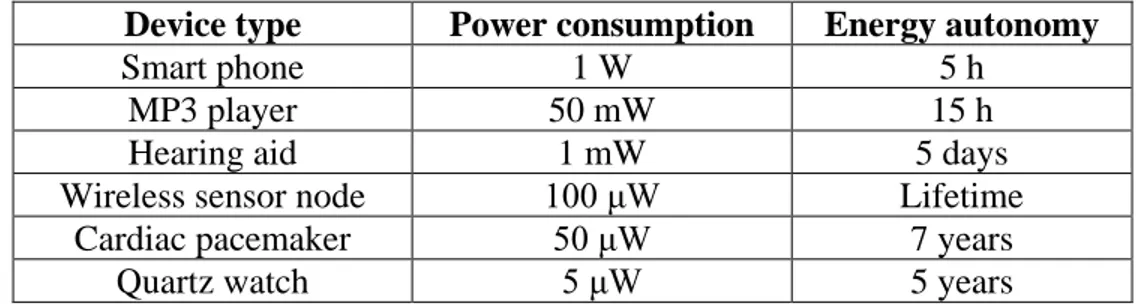
Nowadays, batteries play the dominant role of energy sources for a broad variety of devices, such like smartphone, MP3 player, quartz watch and implantable medical devices (for example, cardiac pacemaker). The typical autonomy of several battery-powered electronic devices is shown in Table 2.1.
Table 2.1: The typical autonomy of several battery-powered electronic devices, from Vullers et al. (2009)
Device type Power consumption Energy autonomy
Smart phone 1 W 5 h
MP3 player 50 mW 15 h
Hearing aid 1 mW 5 days
Wireless sensor node 100 μW Lifetime
Cardiac pacemaker 50 μW 7 years
Quartz watch 5 μW 5 years
In spite of the fact that energy density of batteries has largely increased and the fact that silicon-based electronic devices have greatly reduced the power consumption, the battery-powered devices mentioned above need to be recharged or replaced at intervals of several years or hours. For example, the battery of cardiac pacemaker is usually out of power after 7 years as shown in Table 2.1. In addition, since the emerging integration technologies enable even smaller electronic systems, the size of the battery becomes constrain. As systems continue to shrink, less energy is needed for certain miniaturized devices, research toward power-autonomous is going on.
The power-autonomous devices do not require any internal power source while extracting the needed power from the ambient robust energy. Many kinds of robust energy can be harvested and extracted:
- Motion, vibration and movement
The three main transduction mechanisms for mechanical EH are electrostatic, piezoelectric and electromagnetic. For typical electrostatic transducer, a variable capacitor structure, whose capacitance changes when the overlap area of two electrodes varies in response to an external movement, will change the voltage across the capacitor,
and thus a current will flow to the external circuit (Wang and Hansen (2014)). Generally in piezoelectric devices, a voltage is generated when the piezoelectric material is under mechanical strain (Hajati and Kim (2011)). And for electromagnetic transducer, the relative displacement of a number of turns of coil generates a magnetic field and then delivers an AC current (Tang et al. (2014)).
- Electromagnetic (RF)
A RF-EH system mainly depends on AC to DC rectifier. Takacs et al. (2014) reported a system which is dedicated for harvesting the RF energy on board of geostationary satellites for health satellite monitoring. Tallos et al. (2014) designed a body-worn ambient RF-EH system which is able to harvest freely available RF energy in an office environment using the 2.45-GHz WLAN band.
- Thermal
The basic TE generator is realized by heating one face of TE module, and cooling the other face. By doing so, an electrical current is generated by connected a load to the end terminals of the TE module. Works proposed by Kishi et al. (1999) was the first thermal EH system being used in customer products.
- Solar and light
Solar EH (SEH) system mainly employs photovoltaic cells to convert the incident photons into electricity. The most critical issue of SEH is the matching between the harvesting components (solar panels) and the energy storage elements (batteries or ultracapacitors) in order to maximize harvesting efficiency. Some well-known SHE systems include, but are not limited to, these two proposed by Simjee and Chou (2006) and Park and Chou (2006).
- Biological
Biological EH has a relatively large range of use. For example, a recently published work proposed by Bandyopadhyay et al (2014) is a system that harvests energy from endocochlear potential, which is a biological potential at around 80mV-100mV inside the mammalian ear and changes either positive or negative in the endolymph depending on a coming sound. The system is able to provide 544pW to 4nW power at output with
a low quiescent power consumption of 544pW. On the other hand, Laursen (2012) reported that a fuel cell made from enzyme-equipped buckypaper electrodes generates electricity when implanted into a snail.
In addition, there are also other types of energy that can be harvested, for example nuclear and tidal energies. But they will not be discussed here, since this Master thesis focus on small-dimension and low-power-consumption electronic devices.
2.2 RF energy harvesting (RF-EH)
Nowadays, the use of radio transmitters in variety of applications, such as mobile telephones, mobile base stations, television/ radio broadcast stations and local wireless networks, keeps increasing. This leads to lots of electromagnetic energy broadcasted from billions of radio transmitters around the world. Almost every public place in an urban area is covered by cellular signals from GSM base station, and it is possible to detect tens of Wi-Fi access points at a single location. The available energy in the ambient air provides an opportunity to harvest that energy. Furthermore, the number of radio transmitters continues to increase. Aware of this fact, we may predict that low-power-consumption miniaturized electronic devices may be powered by ambient RF energy. Thus the research in ambient RF-EH system becomes attractive and promising.
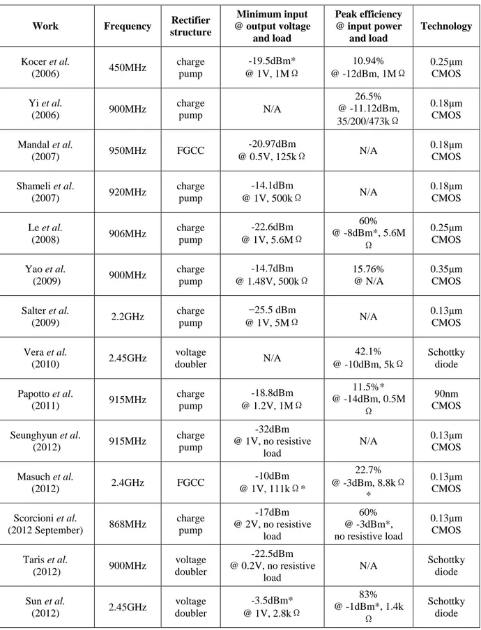
In Table 2.2, some previously published RF energy harvesters, from year of 2006 to now, are presented for readers to have access to a clear literature review on RF-EH systems. As stated in the first chapter, the existing applications of EH are RFID, wireless sensor networks, RF-powered devices and ambient-RF-RF-powered devices. Works done by Li et al. (2013) and Md Din et al. (2012) in Table 2.2 are exactly dedicated for ambient RF-EH. Md Di et al. (2012) report that their harvester on PCB board is able to generate 2.9V to the load (a temperature sensor) with a distance of 50m to a GSM base station antenna tower. Li et al. (2013) designed a RF-EH system with a CMOS rectifier biased by large amount of off-chip resistors. They claim that this system has the same output as in measurement lab when they simply walk outdoors in Maryland campus with it.
It is difficult to make a fair comparison among these works due to the large number of parameters which determine the performance of the harvesters, for example, minimum input
Table 2.2: Comparison of published works (* calculated from graph)
Work Frequency Rectifier structure Minimum input @ output voltage and load Peak efficiency @ input power and load Technology Kocer et al. (2006) 450MHz charge pump -19.5dBm* @ 1V, 1MΩ 10.94% @ -12dBm, 1MΩ 0.25μm CMOS Yi et al. (2006) 900MHz charge pump N/A 26.5% @ -11.12dBm, 35/200/473kΩ 0.18μm CMOS Mandal et al. (2007) 950MHz FGCC -20.97dBm @ 0.5V, 125kΩ N/A 0.18μm CMOS Shameli et al. (2007) 920MHz charge pump -14.1dBm @ 1V, 500kΩ N/A 0.18μm CMOS Le et al. (2008) 906MHz charge pump -22.6dBm @ 1V, 5.6MΩ 60% @ -8dBm*, 5.6M Ω 0.25μm CMOS Yao et al. (2009) 900MHz charge pump -14.7dBm @ 1.48V, 500kΩ 15.76% @ N/A 0.35μm CMOS Salter et al. (2009) 2.2GHz charge pump −25.5 dBm @ 1V, 5MΩ N/A 0.13μm CMOS Vera et al. (2010) 2.45GHz voltage doubler N/A 42.1% @ -10dBm, 5kΩ Schottky diode Papotto et al. (2011) 915MHz charge pump -18.8dBm @ 1.2V, 1MΩ 11.5%* @ -14dBm, 0.5M Ω 90nm CMOS Seunghyun et al. (2012) 915MHz charge pump -32dBm @ 1V, no resistive load N/A 0.13μm CMOS Masuch et al. (2012) 2.4GHz FGCC -10dBm @ 1V, 111kΩ* 22.7% @ -3dBm, 8.8kΩ * 0.13μm CMOS Scorcioni et al. (2012 September) 868MHz charge pump -17dBm @ 2V, no resistive load 60% @ -3dBm*, no resistive load 0.13μm CMOS Taris et al. (2012) 900MHz voltage doubler -22.5dBm @ 0.2V, no resistive load N/A Schottky diode Sun et al. (2012) 2.45GHz voltage doubler -3.5dBm* @ 1V, 2.8kΩ 83% @ -1dBm*, 1.4k Ω Schottky diode
power, the efficiency, the output voltage, the value of the load, the operating frequency, the rectifier topology, the response time, the application, the size of the harvester and discrete components versus microelectronics, the technology cost, the availability, abundance and vicinity of the energy sources, etc. However, it is still possible to compare these presented works to some extent. They can firstly be classified into two parts: harvester on PCB and harvester on chip. Harvesters on PCB employ Schottky diode in a multi-stage voltage doubler topology. The work of Sun et al. (2012) gives a PCE of 81% at -1dBm which is a relatively very high efficiency ever been reported. For harvesters on chip, there are more options of rectifier topologies. Seunghyun et al. (2012) employed charge-pump based rectifier structure and their rectifier generates 1V at -32dBm input which is the
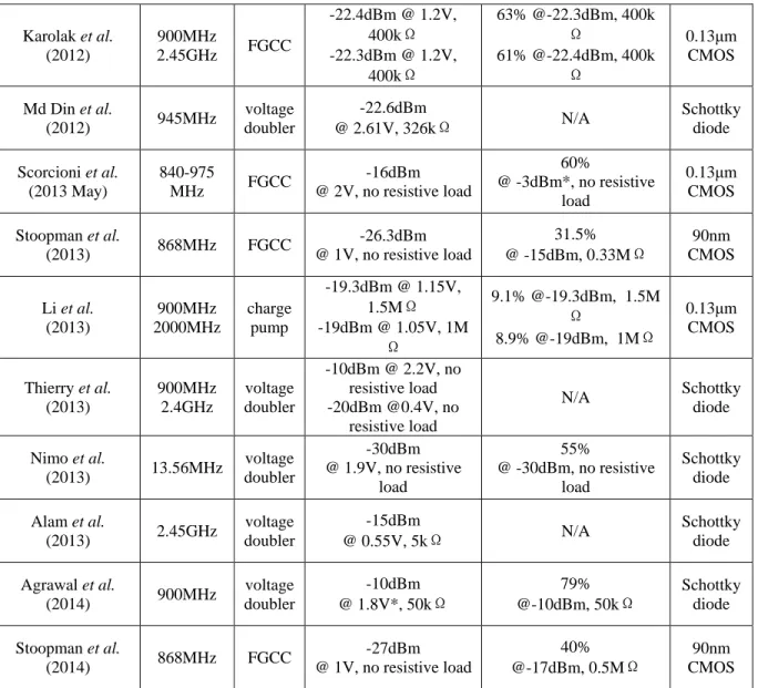
Table 2.3: Comparison of published works (* calculated from graph) (continued)
Karolak et al. (2012) 900MHz 2.45GHz FGCC -22.4dBm @ 1.2V, 400kΩ -22.3dBm @ 1.2V, 400kΩ 63% @-22.3dBm, 400k Ω 61% @-22.4dBm, 400k Ω 0.13μm CMOS Md Din et al. (2012) 945MHz voltage doubler -22.6dBm @ 2.61V, 326kΩ N/A Schottky diode Scorcioni et al. (2013 May) 840-975 MHz FGCC -16dBm @ 2V, no resistive load 60% @ -3dBm*, no resistive load 0.13μm CMOS Stoopman et al. (2013) 868MHz FGCC -26.3dBm @ 1V, no resistive load 31.5% @ -15dBm, 0.33MΩ 90nm CMOS Li et al. (2013) 900MHz 2000MHz charge pump -19.3dBm @ 1.15V, 1.5MΩ -19dBm @ 1.05V, 1M Ω 9.1% @-19.3dBm, 1.5M Ω 8.9% @-19dBm, 1MΩ 0.13μm CMOS Thierry et al. (2013) 900MHz 2.4GHz voltage doubler -10dBm @ 2.2V, no resistive load -20dBm @0.4V, no resistive load N/A Schottky diode Nimo et al. (2013) 13.56MHz voltage doubler -30dBm @ 1.9V, no resistive load 55% @ -30dBm, no resistive load Schottky diode Alam et al. (2013) 2.45GHz voltage doubler -15dBm @ 0.55V, 5kΩ N/A Schottky diode Agrawal et al. (2014) 900MHz voltage doubler -10dBm @ 1.8V*, 50kΩ 79% @-10dBm, 50kΩ Schottky diode Stoopman et al. (2014) 868MHz FGCC -27dBm @ 1V, no resistive load 40% @-17dBm, 0.5MΩ 90nm CMOS
highest sensitivity ever been reported. Scorcioni et al. (2012 September) also employed charge-pump based rectifier and reported a PCE of 60% which is very high compared to other works operating in 900MHz range.
Generally looking at Table 2.2, we may conclude that, to achieve 1V DC output, -22dBm to -10dBm harvested RF power is required. Though the threshold voltage of standard CMOS transistors (e.g. 355mV for nMOS transistor in IBM 130nm technology) is higher than that of a Schottky diode (e.g. 150mV for schottky diode HSMS-2852), the minimum input power of a CMOS-based RF-EH system can also be lower than a PCB-based one by using several threshold cancelation techniques, which will be introduced in the following section. Besides, it should be noted that the value of the load resistor is quite important when talking about output voltage. Normally, the output voltage can be boosted up by the increasing of the load resistance. Thus it is unfair to compare the output voltages of different works without mentioning the load resistance. Furthermore, the devices presented in Table 2.2, working on dual frequencies, have two outputs dedicated for each frequency band separately, which means that there is no power combination of their two bands.
2.3 Ambient RF energy
Visser et al. (2008) claim that in between 25m and 100m from a GSM-900 base station in Netherland, the power density is between 0.1mW/m2 and 1.0mW/m2 (10-5-10-4 mW/cm2) according to their measurement. Pinuela et al. (2013) conducted a citywide RF spectral survey (0.3-3GHz), giving conclusion that GSM900, GSM1800 and 3G are main contributors to the ambient RF power density in London.
As previously stated, Md Din et al. (2012) report their designed harvester is able to generate 2.9V with a distance of 50m to a GSM base station antenna tower and Li et al. (2013) claim that their RF-EH system has output when they simply walk outdoors in Maryland campus with it. Besides, Russo et al. (2013) report that about -26dBm (2.5μW) GSM900 downlink (935MHz-960MHz) power can be harvested in their university building by the 3dBi measuring antenna of spectrum analyzer. They also conducted more measurements at different locations and obtained similar data. Moreover, they demonstrate the possibility of harvesting energy from a ringing phone in near distance.
These results give the fact that it is feasible to harvest ambient RF from GSM base station. But the amount of the harvested power is very small (only 0 to 10μW, if we assumed an antenna with a dimension of 10cm*10cm is used) and only low-power-consumption devices can be supported and driven by such small amount of power.
2.4 Rectifier
The conventional structures of MOS-based rectifier are charge pump, full-wave bridge, FGCC and partially gate cross-coupled (PGCC), which will be all analyzed and discussed in Chapter 3. Some recently published works, relating improvements and modifications on these basic rectifier structures, will be introduced and presented here.
- Improvements on PGCC structure
Ahmadi et al. (2005) adopted Dynamic Bulk Switching (DBS) technique to the PGCC rectifier. As shown in Figure 2.1, the bulks of the diode-connected transistors are connected with the higher voltage, either input or output. This method will effectively reduce the possibility for latch-up. As we know that latch-up is a critical issue for PGCC rectifier, since all the sources of the transistors are connected with the input signals. Ghovanloo and Najafi (2002) use DBS technique not only on the diode-connected transistors but also on the switch-connected transistors. They claim that, by doing so, the substrate leakage current and parasitic components are decreased and the possibility of latch-up is reduced, and efficiency is improved. Note that this conclusion is drawn on the fact that this circuit structure is tested only on 4MHz input AC signal. Using DBS at high frequency levels does not provide great improvements.
Figure 2.1 DBS on diode-connected transistors, from Ahmadi et al. (2005)
Ghovanloo and Najafi (2004) not only employs DBS technique on the diode-connected transistors, but also add additional diodes on the diode-connected transistors sides, as
shown in Figure 2.2 (a). The added parallel diodes help to facilitate the current to flow back to the coil. The same technique is also used in Atluri and Ghovanloo (2007) and Ghovanloo and Atluri (2008).
Bootstrapped capacitor technique is usually used in rectifier design for the purpose of reduce threshold voltage of the transistors. When the rectifier is exploited for an ambient RF-EH system, the threshold cancellation techniques are necessary since the voltage generated on the receiving antenna is relatively low compared with the standard MOS threshold voltage. Lower threshold voltage can not only reduce the “dead zone” of the harvester but also can increase the PCE value due to the smaller voltage drop of the “ON” resistance. Jianyun et al. (2005) and Hu and Min (2005, October) designed a rectifier based on PGCC where the bootstrapping capacitors are connected to the gate of the main pass switches. Authors claim that the voltage drop between the drain and source of the main pass transistor when it is in “ON” state can be close to zero after properly optimize the size of bootstrapped capacitor and the main pass transistor. Thus the PCE is higher compared to the conventional gate cross-coupled rectifier structure under the same load and source conditions. Hashemi et al. (2012) employ both DBS and bootstrapped capacitor techniques, as shown in Figure 2.2 (b), and successfully achieve an increase in PCE. Transistor M5 and M6 form the paths to charge up the bootstrapping capacitors at start up via M7 and M8. The combination of M5, M7 and CB1 reduces the threshold voltage of main transistor M3. DBS technique is employed on transistor M5 and M6 by selectively connecting their bulks to the highest available voltage (either VOUT or input) in order to avoid latch-up, as shown in the right part of Figure 2.2 (b).
- Improvements based on FGCC structure
Theilmann et al. (2010) employs zero-threshold-voltage transistors in FGCC structure in order to push the rectifier to operate into a lower input power level. However, since the threshold is zero, the source-bulk (or drain-bulk) diodes of pMOS transistors will be forward-biased during their “OFF” state. Thus a considerable amount of leakage
current will flow to the ground. To suppress this leakage, authors proposed a version of FGCC rectifier, as shown in Figure 2.3.
Mandal and Sarpeshkar (2007) employ floating-gate techniques to decrease the threshold voltage. This technique is realized by injecting charges into the gate oxide of the transistors, thus a gate-to-source bias voltage is formed to reduce the threshold voltage. This technique is less area-efficient since extra pre-charge circuit is necessary. Furthermore, it is difficult to control the injected charge on the floating gate. The performance of the rectifier may become worse after several years due to the leakage of injected charge (Hashemi et al. (2012)).
(a) (b)
Figure 2.2 (a) DBS and parallel diodes, from Ghovanloo and Najafi (2004). (b) DBS and bootstrapped capacitors, from Hashemi et al. (2012).
- Optimized charge pump structure
Wang et al. (2007) replace the diode-connected MOS transistors in charge-pump based rectifier with a new structure as shown in Figure 2.4 (a). Two auxiliary transistors (Misl and Mis2) as switches are used to update the body voltage of transistor Mi, for the purpose of reducing the body effect in substrate. The threshold voltage of a MOS transistor is a function of the bulk-source voltage (VBS) as a result of the body effect. Diode-connected PMOS Mpi is used to provide bias voltage Vbias for Mi to reduce the threshold voltage.
Le et al. (2008) uses floating-gate techniques to realize threshold cancelation effect to a multi-stage charge pump rectifier. Its single stage is shown in Figure 2.4 (b). Authors Le et al. (2006) proposed a rectifier topology with bootstrapped capacitor technique based on charge-pump topology. It indeed gives higher PCE but it needs large off-chip capacitors and gives small output current.
(a) (b)
Figure 2.4 (a) DBS technique from Wang et al. (2007). (b) Floating-gate technique from Le et al. (2008).
CHAPTER 3
RECTIFIER DESIGN AND POST-LAYOUT
SIMULATION
Rectifier is the most important block of a RF-EH system and should be critically designed because it greatly influences the overall performance of the harvesting system. In this chapter, popular rectifier structures are studied in the first place. Then the designed 3-stage FGCC rectifier dedicated for 880MHz GSM band is presented in the second part. The benefits of employing multiple stages, low-threshold-voltage (LTV) transistors and bulk-GND connection are discussed at the same time. In addition, the layout design of this rectifier is also presented. The post-layout simulation results are given at the end of this chapter.
3.1 Overview of rectifiers: popular CMOS rectifier structures
Diode is the main component in a rectifier, which allows one-way flow of the electrons. In CMOS technology, a PN junction is usually used as a diode for designers. However, it has a typical threshold voltage of 0.7 V, which is apparently too high for the input signal to exceed in our application. In other words, it is not suitable for rectifying low level signals. As we know, schottky diode has very low threshold voltage, low conduction resistance, low junction capacitance and also very large saturation current. However, since conventional CMOS integrated circuits generally do not employ Schottky junction diodes, Schottky diodes are not known to be available in all standard CMOS semiconductor fabrication processes (Ma et al. (2014)). Schottky junction diodes of the prior art require specialized semiconductor fabrication processes, which raises the cost of chip fabrication because extra masks need to be produced by the Fabs which use modular process (Shokrani et al. (2014)). Besides, although the foundries have already began to adopt Schottky diodes into modular process in recent years, accurate model of the schottky diode for simulation are not well prepared and matured enough (Yuan et al. (2015)). Thus schottky diodes in rectifier design are replaced by diode-connected CMOS transistors. However, the voltage needed for turning on the transistor diode is higher than that of a schottky diode. Therefore, transistors working as switches are adopted in some rectifier structures. In this section, different popular CMOS rectifier structures are analyzed. All the recently published advanced rectifiers are derived or improved from these basic and conventional CMOS rectifier structures.
3.1.1 Basic structures of MOS-based rectifier
A: Half-wave structure
The MOS-based half-wave rectifier circuit normally utilizes a single diode-connected MOS transistor, as shown in Figure 3.1. When it is placed in series with the load capacitor across an AC supply, it converts alternating voltage into uni-directional pulsating voltage. It uses half cycles of the applied voltage, either the positive or negative half of the AC wave, and the other half cycle is suppressed because the diode-connected MOS transistor conducts only in one direction.
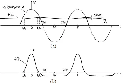
An analysis of one-stage conventional MOS-based half-wave rectifier was presented in Yi et al. (2007) based on the BSIM3 transistor model with appropriate approximations. Figure 3.2 gives the steady-state waveforms of a half wave rectifier. Between t1 and t2, the diode-connected transistor begins to conduct in sub-threshold region. At t=t2, the input voltage rises higher than the output voltage by VTH (threshold voltage of the diode-connected transistor). At this moment, the transistor gets into saturation region. Between t2 and t3, the transistor keeps working in saturation region, and the drain-to-source current of the transistor id(t) equals to(VgsVTH)2. This state continues until the input voltage drops to just higher than the output voltage by VTH at t=t4. Between t3 and t4, the transistor works in sub-threshold region again. Between t4 and t1+T (T is the period of the input AC voltage signal), the drain and source of the transistor are interchanged. The transistor works in sub-threshold region with Vgs 0andVds Vout( )t V tin( ). During this time period, the current id(t) is considered as leakage current Ileak. In the micro-power regime, Ileak cannot be neglected. This is because:
(1) Ileak increases exponentially with the decrease in VTH, and, for low-VTH and zero-VTH devices, Ileak can be of the order of μA and is thus not negligibly small;
(2) Ileak is comparable to the load current in micro-power rectifiers;
(3) the power consumed by Ileak is significant as the transistor stays in the reverse-biased region for a considerable period of time. (Yi et al. (2007))
Half-wave topology is simple and easy to be understood. However, it is not efficient because it uses only the half of the input signal cycle. For low-power-consumption electronic devices, half-wave topology is not the best choice.
Figure 3.1 Conventional MOS-based half-wave rectifier
Figure 3.2 Waveforms of the conventional MOS-based half-wave rectifier from Yi et al. (2007): (a) Waveforms of input and output voltages, (b) Waveforms of transistor current.
B: Full-wave bridge structure
The full-wave rectifier is a little more complicated than the half-wave one. It utilizes both halves of the input AC waveform to provide an output. This greatly improves the efficiency and leads the output to be much easier to be smoothed. The full-wave bridge nMOS-based topology is presented in Figure 3.3.
Taking this circuit as an example, during the positive half cycle of the supply, diodes N3 and N2 conduct in series while diodes N4 and N1 are reverse biased and the current flows through
the load from top to bottom. During the negative half cycle of the supply, diodes N4 and N1 conduct in series, but diodes N3 and N2 switch "OFF" as they are now reversed biased. The current flowing through the load has the same direction as that of the positive half circuit. As the current flowing through the load is unidirectional, the voltage developed across the load is also unidirectional.
The bulk of the nMOS transistors in Figure 3.3 are connected to the rectifier output. This bulk biasing method leads to latch-up hazard, and leakage current Ileak during “OFF” state, same as what we discussed earlier in the half-wave topology section. To overcome the disadvantages, Onizuka et al. (2006) use DBS technique to reduce the undesirable body effect of the main diode-connected PMOS transistor, as presented in Figure 2.1.
The efficiency of full-wave rectifier is higher than the half-wave one, but it is still limited by the voltage drop of two diodes in each single cycle, especially in low-voltage applications.
Figure 3.3 Conventional MOS-based full-wave bridge rectifier (nMOS transistors are used)
3.1.2 Advanced bridge MOS-based rectifiers
As we saw in the previous section, conventional full-wave bridge rectifier uses two pairs of diode-connected MOS transistors. The effective turn-on voltage of the diode-connected MOS transistor is almost equal to the threshold voltage of the MOS transistor, which is smaller than a PN-junction diode, but generally larger than a Schottky diode. Since a pair of diodes turns on at each cycle in series with the input RF signal, the output voltage is twice as low as the threshold voltage of the MOS transistor below the amplitude of the input RF signal. Therefore, in such structure, high PCE cannot be achieved. In order to get high PCE, several advanced rectifier topologies have been proposed.
vin+ vin-Cload Rload N1 N2 N3 N4 Vout
A: Partially Gate Cross-Coupled structure (PGCC)
In partially gate cross-coupled structure, two diode-connected transistors in conventional full-wave bridge structure are replaced by two cross-coupled transistors (N1 and N2) as shown in Figure 3.4. During the positive half cycle, only diode N3 and switch N2 turn on. The current goes out of node Vout from terminal Vin+ through diode N3 and flows through the load Rload. Then the current goes back to terminal Vin- from the load through switch N2. Ground acts as a reference voltage. During the negative half cycle, diode N4 and switch N1 turn on. At this time, the current goes out of node Vout from terminal Vin- through N4 and flows through the load. Then the current goes back to terminal Vin+ from the load through N1. In each case, the negative terminal of the source is connected to the ground and the positive terminal transfer the positive voltage to the output. A DC voltage is generated across the load resistor.
The advantage of this topology comparing with the conventional diode-connected full-wave topology is that the voltage drop across the switch transistors can be lower than threshold voltage if they are properly sized. Thus DBS technique is adopted in some works as we introduced and presented in section 2.4. However, the switch transistors lead to substrate leakage and possible latch-up.
Figure 3.4 Partially gate cross-coupled rectifier (nMOS transistors are used)
B: Fully Gate Cross-Coupled structure (FGCC)
As shown in Figure 3.5, this circuit has a cross-coupled differential CMOS configuration with a bridge structure. In this rectifier, all the four transistors are used as switches.
vin+
vin-C
loadR
load N1 N2 N3 N4V
outWhen Vin+ is high and Vin- is low (during the positive half of the switching cycle), transistor P1 and N2 are on and P2 and N1 are off, assuming that Vin+ and Vin- are large enough to turn the transistors on and off. Current flows out of Vout through P1 and flows into negative terminal of the source through N2. During the other half of the cycle, P1 and N2 are off and P2 and N1 are on. In this case, current flows out of Vout through P2 and flows into positive terminal of the source through N1. Therefore, a DC voltage is generated across the load resistance.
In this circuit, the on-resistance of the transistors is decreased by increasing gate-source voltage (|VGS|) of the transistors and the reverse leakage is reduced by reversing the polarity of the VGS in the cross-coupled structures. Thus, the PCE of this circuit is higher than those of the previous rectifier circuits.
Figure 3.5 Fully gate cross-coupled rectifier
C: Charge-Pump Based Rectifiers
The charge-pump based rectifier is mostly based on the Dickson's topology. In this topology as shown in Figure 3.6 (nMOS and pMOS complementary version), diode-connected transistors are used as pumping devices. During the negative half cycle, MP2 turns off and MN1 turns on resulting in capacitor C being charged to |Vin|. When Vin goes into the positive half cycle, MN1 turns off and MP2 turns on. In this case the charges stored in capacitor C flows into load capacitor CL through MP2, thus the top plate of capacitor C (its right side in Figure 3.6) is pushed up to 2|Vin| and this voltage appears at the output.
Ideally the output voltage should be 2|Vin|, but in fact the output voltage is reduced by the threshold of the rectifying transistors. The output voltage of a single stage charge-pump based rectifier can be expressed as (Dickson (1976)):
vin+
vin-C
loadR
load N1 N2 P1 P2V
out2 ( ) out out inpp TH p p I C V V V C C f C C (3-1)
where Vinpp is the peak-to-peak voltage of the input signal Vin, C is the coupling capacitor as shown in Figure 3.6, Cp is the parasitic capacitor at pumping node, Iout is the average current drawn by the load resistor, f is the frequency of the input AC signal, and VTH is the threshold voltage of transistor.
Figure 3.6 Charge-Pump based rectifier
3.2 Design of a 3-stage FGCC rectifier
3.2.1 Attempt to improve the work proposed by Hashemi et al. (2012)
A high-efficiency CMOS rectifier introduced by Authors Hashemi et al. (2012) was described in section 2.4 and was shown in Figure 2.2 (b). It achieves highly improved efficiency compared to some recently published works which are based on gate cross-coupled structure. It is dedicated for powering biomedical implants in MHz range, thus the sizes of their transistors are optimized to be suitable for application at 3.3V peak input amplitude and 10MHz power transfer frequency using 180nm CMOS technology. Here, this previous work in our Lab Polystim is rebuilt in 130nm CMOS technology and adjusted for low input voltage and GHz range applications.
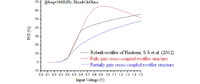
After plenty of parametric simulations, the best performance is found when the size of the main paths transistors (M1-4) is 160/120nm with a multiplier of 50 and the bootstrapping capacitors (CB1-2) are 50pF. The PCE of this structure is obtained and compared with those of fully and partially gate cross-coupled structures as shown in Figure 3.7. The main paths transistors in fully
and partially gate cross-coupled structures have the same size as those in this structure. The frequency of the input AC signal is 1960MHz and the resistive load is 2kΩ.
We can see from the PCE curves in Figure 3.7 that the FGCC structure gives highest PCE at 0.6-1.4V input (peak magnitude) range and after 1.4V the rebuilt rectifier begins to become superior to the others. This is because that the rebuilt rectifier has dynamic bulk switching blocks which effectively prevent latch-up effect at higher input levels. However it is because of the use of dynamic bulk switching blocks, and also because of the use of bootstrapped capacitors, the
rebuilt rectifier has large value of parasitic capacitors, which becomes critical at high frequency levels. Thus its efficiency at 0.6-1.4V input is always restricted. By contrary, the FGCC rectifier structure has four transistors working as switches, which are highly sensitive to turn “ON” or “OFF” at low input power (LIP) levels. Hence it shows high efficiency in 0.6-1.4V input range. In this work, we are focusing on LIP use, which means that the magnitude of the input signal will be no more than 1V, maybe even lower than 50mV. Thus only the case that the magnitude of the input is lower than 1V needs to be concerned. So in this master project, fully gate cross-coupled rectifier, also known as self-driven synchronous rectifier, is adopted due to its remarkable higher PCE at LIP levels comparing with other MOS-based structures.
Figure 3.7 PCE of the rebuilt rectifier of Hashemi et al. (2012) and comparison with those of fully and partially gate cross-coupled structures
3.2.2 Analysis of single-stage FGCC rectifier
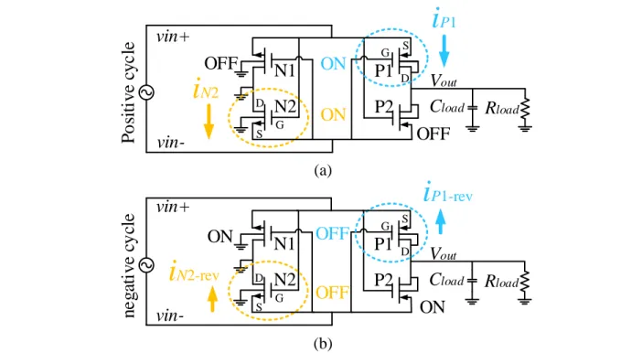
As shown in Figure 3.8, a single-stage FGCC rectifier consists of two NMOS (N1, N2) and two PMOS (P1, P2) transistors. A differential input AC signal is fed to this circuit. In order to better illustrate its operation, the differential input signals (vin+, vin-) and currents through P1 and N2 (iP1, iN2), which are derived from simulation results, are given in Figure 3.9.
The operation of this circuit can be summarized as follows. During the positive half cycle of the input AC signal, for example at point A in Figure 3.9, transistors P1 and N2 are “ON” and P2 and N1 are “OFF”. Current flows out of “Vout” to the load through P1 from the positive terminal of the input source and flows back to the negative terminal of the input source through N2, as indicated in Figure 3.8 (a). By doing this, a DC voltage is generated across the load. Here P1 and N2 work in linear region as two switches. Currents through P1 or N2 can be expressed as:
Figure 3.8 Operation of P1 and N2 of single-stage FGCC CMOS rectifier: (a) Conduction on linear mode (point A in Figure 3.9), (b) Conduction on subthreshold mode (point B in Figure
3.9).
vin+
vin-C
loadR
loadN1
N2
P1
P2
i
P1i
N2i
N2-revi
P1-revV
out G D G S DON
ON
OFF
OFF
OFF
OFF
Svin+
vin-C
loadR
loadN1
N2
P1
P2
V
out G D G S DON
ON
SP
o
si
ti
v
e
cy
c
le
n
e
g
at
iv
e
cy
cl
e
(a) (b) _ 1/ 2 2 1/ 2 1/ 2 0 _ 1/ 2 _ 1/ 2 _ 1/ 2 _ 1/ 2 1/ 2 [( ) ( ) ] 2 DS P N P N P N P N ox GS P N TH P N DS P N P N v W i C v V v L (3-2)where iP1/N2 is the drain-to-source current of transistor P1 or N2 (Ampere); μ0-P1/N2 is the electron
mobility of n- or p-type transistor (cm2·V-1·s-1); Cox is the gate-oxide capacitor per unit area (F/cm2);
WP1/N2 and LP1/N2 are effective channel length and width of P1/N2 respectively (μm); VTH-P1/N2 is
the threshold voltage of P1/N2 (V); vGS-P1/N2 and vDS-P1/N2 are gate-to-source and drain-to-source
voltage of P1/N2 respectively. Transistors P2 and N1 work in the same way during the negative half cycle since this circuit has a symmetrical structure. Therefore, we only discuss transistor P1 and N2 here.
We may easily draw one conclusion from Eq.(3-2) that lower threshold voltage will give larger iP1/N2. In other words, lower threshold voltage will make the transistors transfer the current
to the load more easily during their “ON” mode, which may lead to a higher PCE. The on resistance of transistor P1 or N2 (rON-P1/N2) can be derived from Eq.(3-2):
We may draw the second conclusion from Eq.(3-3): larger width/length ratio may decrease the on resistance, meaning that the voltage drop across the conducting transistor will decrease, which may improve the PCE. PCE is defined by:
Figure 3.9 Theoretical analysis of single-stage FGCC rectifier
V o lt ag e (mV ) Cu rre n t (uA ) 0.0
i
N2i
P1 250.0 500.0 750.0 1000.0 0.0 2.5 5.0 7.5 10.0 12.5 -2.5 -250 24.6265 24.627 24.6275 24.628 24.6285 Time (us) B A A A B vin-vin+ 1/ 2 1/ 2 _ 1/ 2 1/ 2 0 _ 1/ 2 _ 1/ 2 _ 1/ 2 _ 1/ 2 _ 1/ 2 1 ( ) ( ) ( ) P N P N ON P N P N P N ox GS P N TH P N DS P N DS P N L W r i C v V v v (3-3)(3-4)
where T is the period of the input AC signal. However, note that we are discussing the transistors working on “ON” mode and in linear region (for example at point A in Figure 3.9). Later, when the magnitude of vin+ falls, for example, to point B in Figure 3.9, the advantages of low threshold and large width/length ratio transform into disadvantages.
In the shadow area in Figure 3.9, vin+ falls to a smaller value which makes [(vGS-N2) - V TH-N2] 0 and [(vGS-P1) - VTH-P1] 0. Considering from the perspective of a switch, in this case,
transistor P1 and N2 get into “OFF” mode. Ideally, it is supposed to have no current going through them. However, since P1 and N2 operate in weak inversion region, there is a small subthreshold current going through them, as illustrated in Figure 3.8 (b). This small current iP1/N2-rev, flowing in
the reversed direction of the previous working mode, can be expressed by:
(3-5)
where k is Boltzmann constant; T is the absolute temperature; q is the electron charge; n is subthreshold slope factor; ID0 is a parameter related to process. In this situation, both larger
width/length ratio and low threshold voltage provide convenience for this reversed small current to go through, which reduces the total charge delivered to the load, resulting lower efficiency.
In conclusion, the design of FGCC rectifier should make trade-off between “ON” current and reversed subthreshold current by carefully selecting the size and threshold voltage of the transistors.
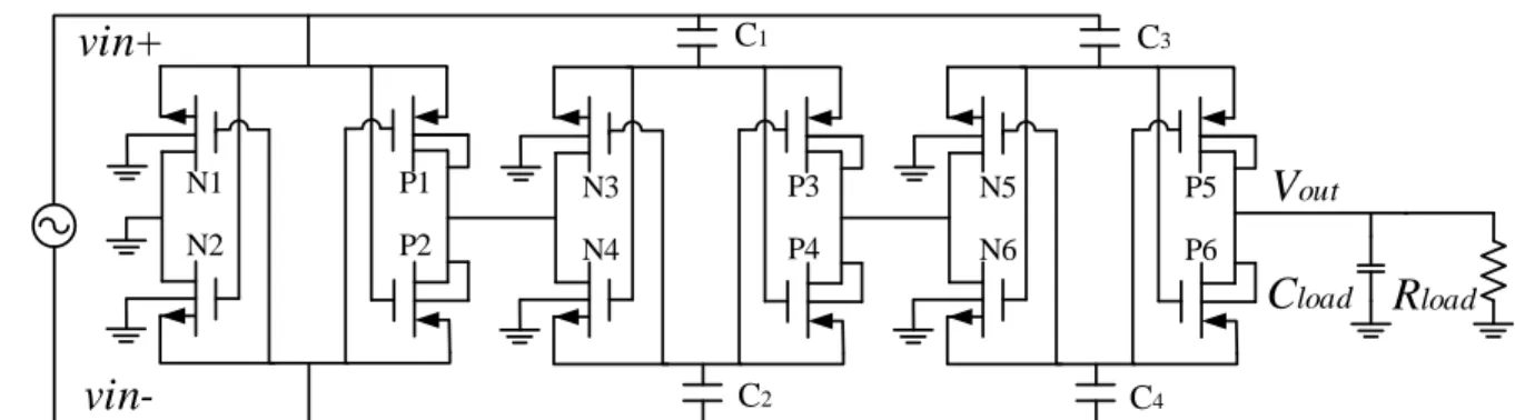
3.2.3 Necessity of cascading stages of the FGCC rectifier
Since the maximum output DC voltage can be obtained from a single-stage rectifier is limited, more stages are needed to produce a higher DC voltage across the load resistor. However, increasing the number of stages causes more leakage because: (a) body bias on nMOS transistors in later stages increases with the number of stages, which may reduce the “ON” charging current
_ 1/ 2 1/ 2 1/ 2 _ 0 1/ 2 exp ( / ) GS P N P N P N rev D P N v W i I L n kT q 0 0 2 / , ( ) ( ) 1 ( )
out out load
in t T in in in t P V R
PCE v vin vin
P v i dt T
through these nMOS transistors, thus pulls down the PCE, and (b) the total number of transistors also increases which apparently augments the total reversed subthreshold current (may vary from several nW to tens of nW depending on the input power, Yi et al. (2007)), thus PCE decreases.
In this work, we expect to have an output to be around 1V to 1.2V at the output. However, the available magnitude of the input signal in front of the rectifier depends not only on the antenna but also on the matching network. If we assume a 350mV magnitude of the input signal can be obtained, after plenty of simulation, three is selected as the number of stages since 3-stage rectifier gives enough output DC voltage and at the same time it does not lead to too much power loss, as shown in Figure 3.10. Another reason for choosing number 3 is that, according to some published works, single-stage and 3-stage FGCC rectifiers are reported to have a peak efficiency higher than 60%. The efficiency cannot be remained this high when the number of stages exceeds five due to the leakage. For example, the 5-stage FGCC rectifiers developed by Le and Luong (2010) and Ouda et al. (2013) have efficiency only around 25% when input power is below 0dBm.
The main role of the four capacitors C1-4 is to prevent the generated DC signals at the outputs of each rectifier stage from flowing back to the input. There is no capacitors at the first stage, since the output voltage at the output of the first stage is lower than the magnitude of the input signal. Thus there is no need to prevent the reverse flowing. This explains why for some designed single-stage FGCC rectifier, no capacitor is used in the input path. In addition, the sizes of the transistors do not need to be the same in each stage. Simulation results show that adjusting pMOS transistors to be slightly larger than nMOS transistors and making the transistors in first stage larger than the others help to improve the efficiency.
Figure 3.10 Proposed three-stage FGCC rectifier
vin+
vin-C
loadR
load N1 N2 N3 N4 N5 N6 P1 P2 P3 P4 P5 P6V
out C1 C3 C2 C43.2.4 PCE comparison of 3-stage FGCC rectifiers using various transistors
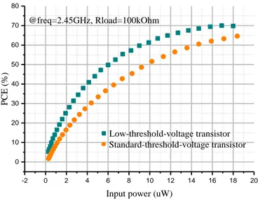
The device library of IBM130nm CMOS8RF technology provides low-threshold-voltage (LTV) transistors. In this technology, the on-current for standard nMOS is 530μA/μm of the device width, and the standard threshold voltage is 355mV. For LTV nMOS, the on-current is improved to 605μA/μm. Thus a lower threshold voltage of 260mV is achieved. As explained previously, lower threshold voltage may give larger “ON” current, which may help to increase the efficiency. However, the expense of lower threshold is the relatively larger leakage current. Hence, the performance of rectifiers using low-threshold transistors needs to be simulated and explored.
Therefore we built the schematics of one 3-stage FGCC rectifier using LTV transistors and another using standard-threshold-voltage (STV) transistors. Both 3-stage rectifiers have the same transistor sizes and load values. The only different thing is their transistor types. The frequency of the input AC signal is 2.45GHz and the resistive load at the output is 100kΩ. The simulated PCE of the two rectifiers are presented in Figure 3.11. As we can see from their PCE curves, from 0uW to 18uW input, the 3-stage rectifier using LTV transistors apparently improves the efficiency. Note that only the performance of the rectifier at LIP levels deserves to be discussed, since we focus on applications at around several microwatts. Therefore, LTV transistors are adopted in this work motivated by their higher PCE at LIP levels.
-2 0 2 4 6 8 10 12 14 16 18 20 0 10 20 30 40 50 60 70 80 Standard-threshold-voltage transistor Low-threshold-voltage transistor PCE (%)
Input power (uW) @freq=2.45GHz, Rload=100kOhm
3.2.5 PCE comparison of 3-stage FGCC rectifiers using different bulk
connections
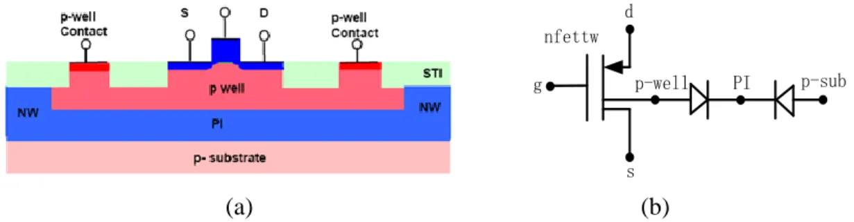
IBM130nm CMOS8RF device library provides LTV nMOS transistors within a p-well that is isolated from the substrate. The cross section of the device is shown in Figure 3.12 (a). Isolation is achieved by inserting a buried n-type layer between the local p-well and the P-substrate. This is a 6-terminal device as shown in Figure 3.12 (b). The isolating n-type layer should be tied to a quiet power supply that is at a high enough potential to prevent forward biasing.
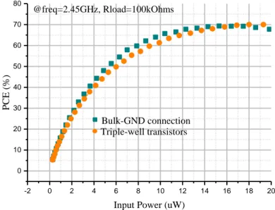
As was previously discussed in section 2.4, latch-up is a critical issue in rectifier design. In order to eliminate the latch-up effect, we may turn to triple-well LTV nMOS transistors instead of standard n-Well LTV nMOS. In order to know if triple-well LTV nMOS would improves the PCE, the schematics of two 3-stage rectifiers, one uses LTV nMOS transistors with bulk-GND connection and another one uses triple-well LTV nMOS transistors with isolating layer connected with the output node, are built and simulated. Both rectifiers have the same transistor sizes and load values. The only different thing is the method of bulk connection. The frequency of the input AC signal is 2.45GHz and the resistive load at the output is 100kΩ.
(a) (b)
Figure 3.12 PI triple well LTV nMOS transistor: (a) Cross section view from IBM Training file, (b) Symbol view.
The simulated PCE of the two 3-stage rectifiers are present in Figure 3.13. We may find out from the PCE curves that the rectifier with bulk-GND connection has slightly higher efficiency from 0uW to 16uW input. After 16uW, it seems to become inferior to the rectifier using triple-well transistors. The reason of this phenomenon is that the output voltage is too low in range of 0-16uW input and the isolating layer is connected with the output with no other choice, thus the triple-well topology does not prevent latch-up at all and in contrary they themselves generate leakage. When the two rectifiers deal with higher input power, rectifier with triple-well transistors effectively
nfettw g
s d
prevents latch-up and as a consequence it gives higher efficiency. However, note that the focus of this project is on LIP use. Therefore, we chose the rectifier using bulk-GND connection.
-2 0 2 4 6 8 10 12 14 16 18 20 0 10 20 30 40 50 60 70 80 PCE (%)
Input Power (uW) @freq=2.45GHz, Rload=100kOhms
Triple-well transistors Bulk-GND connection
Figure 3.13 PCE comparison of 3-stage FGCC rectifier structure using different bulk connection
3.2.6 Design of 3-stage FGCC rectifier
Following the preliminary analysis shown above, we can get to the conclusion that, in order to design a rectifier intended to operate with several microwatts of input power, and having a higher efficiency at low power levels, a FGCC structure, composed of three stages in series, and based on LTV transistors, and bulk-GND connection for nMOS transistors.
Figure in APPENDIX B shows the resulting 3-stage FGCC rectifier built in Virtuoso Schematic Editor. Power excitation is an 880MHz AC source with zero port resistance. By carefully selecting the transistor sizes, we obtained good performance.
3.2.7 Layout design
The layout is designed in Virtuoso Layout Suite Editing, using IBM 130nm cmrf8sf Technology with MA last metal Back End Of Line (BEOL) Metallization Options. The cross section of this MA last metal Option is presented in APPENDIX A.
- Layout of transistors
As shown in Figure 3.14 (a), the gate of nMOS transistor is connected with Metal One (M1) at both of its two ends, in order to have low resistance gate connection. M1 forms a gate contact ring. Then a substrate contact ring is designed just outside of the gate contact ring (p-well tie downs). For the nMOS transistors at the first stage of the rectifier whose sources and drains are connected with the pads, an N-well guarding is designed to collect minority electrons injected into the substrate.
As shown in Figure 3.14 (b), the pMOS transistor also has a gate contact ring. And an N-well contact ring is designed right outside the gate contact ring. This N-well is tied down by a n+/P-well diode in order to prevent N-well potential from rising too high to the P-substrate by providing the reverse biased leakage path, as explained in IBM cmrf8s Design Manual.
(a)
(b)