LOW-COST INTEGRATED WAVEGUIDE ANTENNA FRONT-END
SOLUTIONS FOR FIFTH GENERATION CELLULAR SYSTEMS AND
BEYOND
AJAY BABU GUNTUPALLI
DÉPARTEMENT DE GÉNIE ÉLECTRIQUE ÉCOLE POLYTECHNIQUE DE MONTRÉAL
THÈSE PRÉSENTÉE EN VUE DE L’OBTENTION DU DIPLÔME DE PHILOSOPHIAE DOCTOR
(GÉNIE ÉLECTRIQUE ) DÉCEMBRE 2014
UNIVERSITÉ DE MONTRÉAL
ÉCOLE POLYTECHNIQUE DE MONTRÉAL
Cette thèse intitulée :
LOW-COST INTEGRATED WAVEGUIDE ANTENNA FRONT-END
SOLUTIONS FOR FIFTH GENERATION CELLULAR SYSTEMS AND
BEYOND
présentée par : GUNTUPALLI Ajay Babu
en vue de l’obtention du diplôme de : Philosophiae Doctor a été dûment acceptée par le jury d’examen constitué de :
M. KASHYAP Raman, Ph. D., président
M. Wu Ke, Ph. D., membre et directeur de recherche M. FRIGON Jean-François, Ph. D., membre
ACKNOWLEDGMENT
I would like to thank my PhD research director, Prof. Ke Wu for giving me the opportunity to pursue my Doctorate study at Ecole Polytechnique of Montreal. His motivation helped me to understand and think solutions for some of the bottleneck problems in millimeter-wave communication.
I would like to thank technical personnel Mr. Jules Gauthier, Mr. Steve Dubé, Mr. Traian Antonescu and Mr. Maxime thibault in Poly-grames Research Centre for realizing the simulated prototypes. I would like to thank Mr. Jean-Sébastien Décarie for assistance with software problems and also Mrs. Ginette Desparois and Mrs. Nathalie Lévesque for administrative procedures of the department.
I would like to my master thesis director Prof. Substrata Sanyal at Indian Institute of Technology, Kharagpur (IIT-KGP) for teaching me RF and microwave basics and motivating me to choose my career in the microwave field. I specially want to thank Dr. Mrinal Kanti Mondal and Dr. Priyanaka Mondal for helping me to settle in Montreal and for all the encouragement. My special thanks go to my master thesis co-supervisor Dr. Vamsi Krishna Velidi for teaching me microwave filter design.
I specially want to thank Dr. Tarek Djerafi for introducing me to millimeter-wave frequency antenna array design. I would like to thank my friends Divyabrahmam Kandimalla (at IIT-KGP), Dr. Nasser Ghasemi, Dr. Sulav Adhiakri, Dr. Farshad Sarbachi, Dr. Shabnam Ladan, Lydia Chioukh, Pascal Burasa, Ya Deng, Babak Nikfal, Dr. Ali Doghri, Yang Ping, Tariq sha Mohammed, who made my stay at Poly-Grames Research Center memorable. I would like to thank Pascal Burasa and Bilel Mnasri for helping me to write the French version of Abstract.
I specially would like to thank Dr. Shabnam Ladan for her great help in revising my PhD thesis. Dr. Ladan was very helpful and supportive during my PhD. The ideas we shared during common discussion were significantly improved the quality of thesis.
Finally, I would like to extend my gratitude to my mother Rani Guntupalli and father Satyanayana Guntupalli who supported my decision at every stage of my life and encouraged to pursue Ph.D. degree in Canada. I would like thank my sister Vijaya sri Guntupalli, brother-in-law Naveen kode and my niece Kundana for all their encouragement during my graduate studies. I also want to thank my extended family members Vanaja Guntupalli, Sethaiah Vootla, Vijay anna, Laxmi vadina for all support during the final stage of writing of PhD thesis.
d’antennes ayant des gains importants dans la bande de fréquences millimétriques. Ces antennes basées sur des structures guide d’onde présentent de très bonnes performances mais elles sont difficilement intégrables avec les composants actifs. Dans la bande millimétrique, la technologie GIS (guide d’onde intégré au substrat) représente une excellente alternative pour la conception et l’implémentation des réseaux d’alimentation à faible couts et a faibles pertes. Les antennes alimentées à l’aide des structures GIS sont capables d’offrir une excellente efficacité de radiation ainsi qu’une large bande d’opération. Dans cette thèse, la technologie GIS a été choisie dans le but de concevoir des réseaux de distribution de puissance et de phase dans le but d’implémenter des antennes a grande efficacité.
Les contributions scientifiques principales de cette thèse peuvent être divisées en deux catégories. La première partie étant consacrée a la présentation des solutions pour des structures a rayonnement efficace tels que les réseaux d’antennes LP, DLP et DCP. Le choix de l’élément rayonnant est une étape vitale et cruciale pour le design de réseaux d’antennes a gain élevé et qui peuvent être contrôlés électroniquement. Dans la deuxième partie de cette thèse, des nouvelles techniques seront proposées dans le but de contrôler la direction du rayonnement suivant plusieurs directions dans les plans d’élévation et azimut.
A la fréquence 60 GHz, l’antenne a diélectrique fuselé a été choisie pour avoir une polarisation rectiligne et l’antenne patch ‘a cavité ont été choisie afin d’avoir une polarisation circulaire. En effet, l’antenne a diélectrique fuselé est utilisée par la suite pour faire la conception d’un réseau d’antennes 4x4 ayant une polarisation rectiligne a un angle de 45o.Ensuite, l’antenne a diélectrique
a été l’unité élémentaire pour l’implémentation d’un réseau a polarisation rectiligne double dont les deux polarisations sont orthogonales ce qui constitue un avantage important par rapport ‘a un réseau a simple polarisation vu qu’on est capable de multiplier par 2 le débit de données a
transmettre par notre nouvelle architecture. Finalement, l’antenne a diélectrique fuselé a été sélectionnée dans le but de concevoir un réseau d’antennes planaire ayant la capacité de faire un balayage unidimensionnel seulement (1-D).
La matrice de Butler BFN a été modifiée et intégrée au sein d’un réseau d’antennes patch 2x2, permettant d’avoir un pattern de polarisation rectiligne dans les plans élévation et azimut simultanément. La matrice de Butler a une taille réduite et permet l’alimentation d’un réseau d’antennes planaire. Le réseau d’antennes est conçu suivant la technique multicouche. Le prototype a été validé expérimentalement autour de la bande de fréquences Ka.
Dans la technique suivante, un faisceau CP est dirigé en 2-D en espace. À 60 GHz, un faisceau circulairement polarisée est obtenu en alimentant une matrice d’antenne patch en utilisant une topologie d’alimentation SIW. Dans un premier temps, les caractéristiques de l'antenne CP sont obtenues par l'insertion de deux encoches sur la circonférence extérieure d'un patch LP. Dans l'étape suivante, une matrice 2 x 2 CP patch, ayant une taille compacte et une excellente performance de rapport axial (AR) est réalisée à 60 GHz. Le faisceau rayonne avec des caractéristiques de CP en élévation et en azimut en utilisant trois dimensions construit à partir de la matrice de Butler. Ce réseau d’antennes est facilement utilisable dans un système radio intelligent.
Les mécanismes de balayage 2-D utilisant la phase et la fréquence simultanément, ont été démontrés dans cette thèse. Dans un premier temps, une technique pour la réalisation de faisceaux directionnels balayant une région limitée, est introduite et implémentée en technologie SIW. Le balayage 2-D est réalisé par le balayage de phase d’une antenne à onde de fuite. Un réseau de faisceau basé sur la lentille Rotman et une matrice de d’antenne à onde de fuite sont intégrés sur le contour de sortie, pour réaliser un réseau d'antenne de balayage 2-D.
Dans la dernière technique, une matrice d’antenne à balayage 3-D (toute l’espace) est proposée pour couvrir une région de 320ᵒ en azimut et 20ᵒ en élévation. Dans cette configuration, l'un des faisceaux peuvent être utilisé pour l’émission tandis que l'autre faisceau est simultanément utilisé pour la réception. Dans la phase finale, la plage de balayage du faisceau est en outre étendue pour couvrir toute l’espace en plaçant deux MBAs indépendants et orthogonales l’un à l'autre. La
les brevets américains (en attente), des revues internationales de haut niveau et également présentés lors de conférences internationales tenues en Amérique du Nord, Europe et Asie-Pacifique.
ABSTRACT
Millimeter-wave (or simply mm-wave) antenna arrays with single linear polarization (LP), dual linear polarization (DLP) and dual circular polarization (DCP) characteristics are widely being used for numerous applications including wireless data communication, radar sensors, passive imaging, energy harvesting and cognitive radio systems. Among different types of feeding structure, waveguide presents an excellent candidate to implement low-loss feeding networks and high-gain antenna arrays over mm-wave frequency range. Those waveguide-based antennas have been exhibiting excellent radiation characteristics, but they are not easy to integrate with active components. At mm-wave frequency, SIW (substrate integrated waveguide) is an emerging outstanding candidate to implement low loss and low cost feeding networks. SIW-fed antenna is able to yield high radiation efficiency and broadband impedance behavior. In this thesis, SIW feeding transmission technology is chosen to implement power and phase distributing networks for realizing high efficiency antenna front ends.
The main scientific and technical contributions can be summarized into two parts. In the first part, solutions for efficiently radiating apertures have been proposed such as high gain LP antenna arrays, pencil beam antenna arrays, DLP antenna arrays and DCP antenna arrays. The radiating element choice with excellent radiation characteristics is vital in realising high gain antenna array and electronically steerable phased arrays. In the second part, new techniques have been proposed to steer the fixed beam into multiple directions in elevation and azimuth utilizing passive phase shifting network.
At 60 GHz frequency, dielectric rod antenna is selected for linearly polarized radiation and cavity backed metallic circular patch antenna is selected to obtain circular polarization radiation. Single rod antenna element is experimentally characterized to validate the proposed concept. In the next stage, high gain antenna array with 45o linear polarization utilizing rod antenna radiating element
is demonstrated and feeding implemented in three dimensional (3-D) architecture is integrated along with the 4 × 4 antenna array. The data handling capability of single polarization antenna array is increased up to two fold by integrating two orthogonal polarized antenna arrays with an aperture area of one single polarized array. The Rod antenna application is also extended to obtain phase steered beams in horizontal plane in a planar 1-D phased array antenna configuration. The
In the next technique, CP beam is steered in 2-D scans space. At 60 GHz frequency, circularly polarized radiated beam is obtained by feeding an array of patch antenna using SIW feeding topology. At first, CP antenna characteristics are obtained by inserting two notches on the outer circumference of a LP patch. In the next stage, 2 x 2 CP patch array occupying compact size and excellent axial ratio (AR) performance is realized in the SIW technology. The radiated beam with CP characteristics is phase steered in elevation and azimuth using three dimensionally constructed Butler matrix BFN. The two dimensional scan CP phased array antenna system is readily usable to implement antenna front end in a cognitive radio system.
The 2-D scan mechanisms utilizing phase and frequency scan simultaneously have been demonstrated in the work. In the first technique, a technique for achieving simultaneous multiple scanned directional beams limited scan region is introduced and its development is enabled by the substrate integrated waveguide (SIW) technology. The 2-D scanning is achieved by phase steering each beam of frequency scanned leaky wave array. Rotman lens based BFN and array of LWA sources are integrated on the output contour to realize the 2-D scan conformal phased array antenna. In the last technique, full-space scanning 3-D phased array antenna is proposed to cover 320ᵒ scan region in azimuth and 20ᵒ scan region in elevation. Two-layered feed part is implemented by the combination of 90º H-plane coupler and two similar 4 × 4 Butler matrices. In this configuration, one of the beams can be used for transmit operation while the other beam can be used for receive operation simultaneously. Measured S-parameters and directional pattern measurements have confirmed the multi-dimensional scanning capability of the proposed MBA. In the final stage, the beam scanning range is further extended to cover the full-plane region by placing two independent MBAs orthogonal to each other. The proposed technique is scalable for various system applications up to W-band frequency range and beyond.
In this PhD thesis, complete set of antenna front-end solutions are proposed and validated in a low-cost integrated waveguide technology for future 5th generation cellular communication. The
comprehensive study of the antenna techniques are discussed in detail in PhD thesis. The antenna radiating part is designed and simulated in full-wave electromagnetic software Ansoft high simulation software (HFSS) and experimentally verified in far-field MI technology anechoic chamber. The results presented in this PhD thesis are published in US patents (pending), reputed international journals and also presented in international conferences held in North America, Europe and Asia-Pacific regions.
TABLE OF CONTENTS ... XI LIST OF FIGURES ... XV LIST OF TABLES ... XXIV LIST OF APPENDICES ... XXV LIST OF ACRONYMS AND ABBREVIATIONS ... XXVI
INTRODUCTION ... 1
Background and Motivation ... 1
1.1.1 Benefits of Phased Arrays ... 10
Outline of thesis ... 11
CHAPTER 2 MILLIMETER-WAVE ANTENNA ARRAY AND PHASED ARRAY ANTENNA WITH LINEAR POLARIZATION DIVERSITY ... 13
60 GHz Planar Dielectric Rod Antenna ... 13
2.1.1 Antenna design ... 14
2.1.2 Antenna radiation pattern performance ... 19
45o linearly polarized high gain antenna array for 60 GHz radio ... 22
2.2.1 3-D Antenna array design ... 24
2.2.2 Vertical InterConnect ... 24
2.2.3 Feed network of 4×4 planar array ... 26
2.2.5 Impedance and radiation performances ... 31
Milli-meter wave linear polarization diversity antenna array at 35 GHz ... 33
2.3.1 Radiating element performance ... 35
2.3.2 Feed network performance of HP and VP arrays ... 35
2.3.3 HP linear array performance ... 38
2.3.4 VP linear array performance ... 38
2.3.5 DLP array performance ... 40
Polarization Diversity Antenna with High Gain and Small Foot Print for Millimeter-wave Inter-Satellite Communication at 60 GHz Frequency ... 43
2.4.1 Feed network performance of HP and VP arrays ... 44
2.4.2 DLP array architecture and fabrication ... 47
2.4.3 HP linear array performance in the DLP array radiating environment ... 52
2.4.4 VP linear array performance in the DLP array radiating environment ... 53
2.4.5 HP and VP linear array peak gain ... 55
Planar 1-D Scan Phased array antenna at 60 GHz ... 55
Conclusions of rod antenna applications ... 58
CHAPTER 3 TWO-DIMENSIONAL SCANNING ANTENNA ARRAY DRIVEN BY INTEGRATED WAVEGUIDE PHASE SHIFTER ... 60
Single element design and characterization ... 61
Beamforming network design ... 62
3.2.1 BFN S-parameter performance ... 67
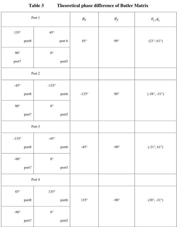
3.2.2 Theoretical beam pointing angles ... 67
3.2.3 2×2 Antenna Array beamforming results ... 70
POLARIZATION DIVERSITY ... 77
60 GHz Circularly Polarized Antenna Array Made in Low-Cost Fabrication Process . 77 4.1.1 RHCP antenna Element ... 79
4.1.2 RHCP array ... 81
Dual Circular polarization antenna element ... 88
4.2.1 Antenna element and feeding network design] ... 88
4.2.2 Axial ratio performance ... 92
4.2.3 DCP element radiation performance ... 93
Phase steered circularly polarized radiated beam in 2D scan space ... 94
4.3.1 Beam forming network design ... 94
4.3.2 Antenna array design ... 100
4.3.3 Measured phased array performance ... 102
4.3.4 CONCLUSION ... 104
CHAPTER 5 PHASED ARRAY ANTENNA DESIGN WITH TWO DIMENSIONAL SCAN CAPABILITY ... 106
Conformal Multi-Beam Integrated Waveguide Array Antenna with Two-Dimensional Scanning Capability ... 106
5.1.1 SIW leaky wave antenna ... 109
5.1.3 SIW cavity coupled E to H plane bend ... 117
5.1.4 2-D scan conformal antenna results ... 121
Simultaneous Transmit/Receive Full-Space Scanning Phased Array System for Future Integrated High Data Rate Communication over E-band and Beyond ... 127
5.2.1 Two-port LWA with 45º inclined polarization ... 128
5.2.2 Millimeter-wave Crossover Structure Utilizing Simultaneous Electric and Magnetic Coupling ... 131
5.2.3 Beamforming network design ... 139
5.2.4 Simultaneous transmit/receive operation ... 145
5.2.5 Full-space scan array with simultaneous transmit/receive operation ... 153
Conclusion ... 155
CHAPTER 6 CONCLUSIONS AND FUTURE WORK ... 157
Conclusions ... 157
Future work ... 161
REFERENCES ... 163
APPENDIX I SMALLEST FOOT PRINT PENCIL BEAM ANTENNA ARRAY ... 176
Figure. 2.2. ALTSA is loaded by a tapered dielectric rod. ... 15
Figure. 2.3. ALTSA antenna impedance matching and gain as a function of frequency. ... 15
Figure. 2.4. ALTSA antenna simulated radiation behavior in E and H-planes at 60 GHz. ... 15
Figure. 2.5. Electric field strength inside the dielectric guide. ... 16
Figure. 2.6. Simulated radiation efficiency (with and without considering metallic and dielectric losses) of the final prototype including the input transition. ... 18
Figure. 2.7. E-plane co-pol and cross-pol radiation pattern as a function of substrate thickness. . 19
Figure. 2.8. (a) Manufactured prototype of the rod antenna. (b) Simulated and measured return losses of the dielectric rod antenna. ... 20
Figure. 2.9. E-plane and H-plane measured co-pol simulation (dotted), measurement (solid) and simulated cross-pol (sash-dot), measured cross-pol pattern (dash) for the rod antenna at 57 GHz, 60 GHz and 64 GHz. ... 21
Figure. 2.10. 45ᵒ rotated vertical interconnect (a) architecture (where Dsh=1.92 mm, S=1.1 mm, Wvia=0.2 mm), (b) performance. ... 25
Figure. 2.11. (a) ALTSA antenna architecture, (b) dielectric rod antenna, where RW=1.2, RL=10, RM=5, L=1.6, LA=5.1, TT=12ᵒ, LM=1.9, W=0.14, S=1.16 and a=1.6 (all dimension are in mm). 26 Figure. 2.12. (a) 3-D view of the feed network, where input port on the XY-plane and 16 output ports are located on the vertically placed waveguides, (where C = 2, 3,…16), W=1.47, D1=3.65, D2=3.36, D3=4.5, H=0.254, S=1.1, M=12.3, and N=14 (all dimensions are in mm), (b) Vector representation of E-field inside the 3-D feed network. ... 27
Figure. 2.13. S-parameters (c) amplitude performance, (d) differential phase between ports P2, P3 and P3, P4. ... 28
Figure. 2.14. (a) Antenna array simulated prototype showing only ALTSA antenna. (b)
Fabricated prototypes of the 16 rod antennas and feeding network, (c) final array prototype. . ... 29 Figure. 2.15. Magnitude of S11 and peak gain comparison between simulated (dotted line) and
measured (solid line) results. ... 30 Figure. 2.16. Antenna radiation pattern at 60 GHz frequency in (a) E-plane (XZ-plane) and (b)
in H-plane (YZ-plane). Dash line: co-pol simulated, solid line: co-pol measured, dotted: cross-pol simulated and dot-dash: cross-pol measured. ... 32 Figure. 2.17. Illustrative diagram showing the operation of simultaneous power and data
communication system. ... 35 Figure. 2.18. (a) The linearly tapered ALTSA antenna and feed portion of the radiating element,
(b) simulated antenna impedance matching as function of frequency and (c) Low side lobe level radiation pattern of the ALTSA antenna. E-plane and H-plane are symmetrical and the cross polarization also shown. ... 36 Figure. 2.19. Feed network part of (a) HP polarization, where the physical parameters are Dx=
0.84λ, Dy= 0.85λ, W=3.3mm, D=0.2mm, Ws=0.508mm, and DL=3.44mm, and (b) VP polarization, where the physical parameters are Dx= 0.84λ, Dy= 0.85λ., S-parameters of the feeding network for (c) HP array, and (d) VP array. ... 37 Figure. 2.20. Simulated power flow inside the DLP array when fed (a) from port 1, and (b) from port 2. ... 39 Figure. 2.21. DLP array (a) architecture in HFSS, and the experimental prototype of (b) single
VP array, and (c) DLP array, (where the horizontal and vertical polarization array are
integrated into single aperture area). ... 40 Figure. 2.22. Measured H-pol array performance at 35 GHz (a) in E plane (b) in H plane, where
simulated co-pol (dotted), measured co-pol (solid) and measured cross pol (dotted dash). .. 41 Figure. 2.23. V-pol array performance at 35 GHz (a) in E plane (b) in H plane, where simulated
co-pol (dotted), measured co-pol (solid) and measured cross pol (dotted dash). ... 42 Figure. 2.24. H-polarized feeding network (a) proposed architecture, (b) S-parameters. ... 44 Figure. 2.25. V-polarized feeding network, (a) architecture (b) S-parameters ... 45
GHz, (c) 62 GHz, where simulated co-pol (dotted), measured co-pol (solid) and measured cross pol (dotted dash). ... 50 Figure. 2.30. Simulated and measured V-pol array performance in E-plane at (a) 58 GHz (b) 60
GHz, (c) 62 GHz, where simulated co-pol (dotted) , measured co-pol (solid) and measured cross pol (dotted dash). ... 51 Figure. 2.31. Simulated and measured peak gain in H-plane for (a) H-pol array only, and (b)
V-pol array only. ... 53 Figure. 2.32. Simulated electric field component for (a) H-pol array only, and (b) V-pol array
only. ... 54 Figure. 2.33. 1-D scan phased array antenna (a) simulated model (Ssiw=1.57,L1=6.58, Laltsa=4.5,
Lant=56,Want= 14,B=3.46, where all dimensions are in mm), (b) fabricated prototype, azimuth plane radiation pattern at 60 GHz frequency (c) simulated, and (d) measured for four input ports P1 to P4 (where P = port number). ... 57
Figure. 3.1. (a) Basic cross section (a-a’) of antenna stack up in XZ – plane (b) Antenna top view and exploded view (W = 2.96, Wv = 0.6, L=3.3, R1 = 0.9, R2 = 2.19, S = 1.15625, Ld = 3.427,
P = 0.5, Dv = 0.254. Where antenna dimension are in mm). ... 62
Figure. 3.2. Simulated reflection coefficient magnitude and peak gain as a function of frequency. ... 63 Figure. 3.3. (a) Planar 4×4 butler matrix with four hybrid couplers and two 45ᵒ phase shifters,
where D1 = 0.19, D2 = 0.32, P1 = 0.9, P2 = 1.47, Ds = 0.47, S = 3.87, W = 2.96, where all dimension are in mm, and (b) Two layer eight port hybrid using two different shape bends.
The coupling slot dimensions are width Wc = 0.16 mm, distance from end wall Sc = 0.275 mm, and length Lc = 2.56 mm. Ports P1-P4 on layer 1 and P5-P8 on layer 2. ... 64 Figure. 3.4. BFN (a) Simulated transmission coeffceints fed from port 1, and (b) differential phase for all four ports, the blue dotted curve is the differencial phase shift between two bends. Here,
P is the input port number. ... 65
Figure. 3.5. Co-ordinate system definition (a) on 0ᵒ degree rotated array, and (b) on 45ᵒ degree rotated array. ... 68 Figure. 3.6. Ka-band phased array (a) Basic cross section of array stacked up (a-a`) (where the
BFN is synthesized on layer 1, 2, foam is on layer 3 and antenna is integrated on layer 4), and (b) Experimental proof-of-concept prototype, multi-layered diagram and 2-D scanned beams. ... 69 Figure. 3.7. Measured reflection coefficient for port 1 and isolation from 1 to 2, 3 and 4. ... 70 Figure. 3.8. (a) Simulated normalized E plane radiation patterns as a function of θ (in degrees)
when fed from port 1, and (b) comparison between simulated and measured normalized H plane radiation patterns as a function of (in degrees) when fed from port 1 at 26.5 GHz. 71 Figure. 3.9. Measured normalized H plane radiation patterns as a function of (in degrees) when fed from (a) port 2, and (b) port 3. ... 71 Figure. 3.10. Simulated 3-dB beam widths at 26 GHz. ... 72 Figure. 4.1. CP antenna. (a) Top view, (b) exploded view and (c) cross section view. Where the
parameter dimensions in mm are Wvia= 0.25, Rvia= 0.25, Wa=3.5, Wb=3.5 Wv=0.25, Wcd=0.3, Wt=0.3, Lt=0.375, Wn=0.4, Ln= 0.4, R=0.75, Of=0.49, Ws=0.33, Ls=1.9, and Wsiw=1.37. ... 78 Figure. 4.2. Axial ratio as a function of frequency for different values of tuning stub (a) length, and
(b) width, (c) magnitude of S11 and peak RHCP gain, and (d) antenna radiation pattern in standard cut at 60 GHz. ... 80 Figure. 4.3. (a) Power dividing network for 2 × 2 patch array, (where Wp=0.25mm, Wv=0.27mm,
X=0.3mm, P= port number), (b) S-parameters as a function of frequency (solid line: |S11|). 81
Figure. 4.4. RHCP array. (a) Three dimensional view, and (b) experimental prototype top view and with end launch connector. ... 82
phase shifter, (c) side view , and (d) back view,.(where the parameters (in mm) are Ln=1.2, C=0.35, Wsiw=1.4, WC=0.34, LC=1.7, H = 0.635,WV =0.45, Want =2.4, and Wfeed =1.2). ... 89 Figure. 4.9. DCP feed network (a) amplitude, and (b) phase performance. ... 90 Figure. 4.10. .. Experimental prototype of DCP antenna………91 Figure. 4.11.Axial ratio as a function of frequency (a) for three radiating angles, and (b) in LHCP
mode. ... 92 Figure. 4.12.Antenna LHCP gain at 60 GHz in (a) xz-plane, (b) yz-plane. Dash line: simulated,
solid line: measured. ... 93 Figure. 4.13.(a) Proposed vertical interconnect, (Wvc=1.7mm, Svia=0.92mm, Wvia=2.3mm), (b)
frequency response, ... 95 Figure. 4.14.(a) BFN 3-D architecture, (b) BFN field distribution inside the integrated waveguide
topology when fed from port 1, BFN (c) vertical guide part (where Wsiw=1.7 Wfeed=1.7, Want= 1.7, S= 0.76,D=0.4, L=2.4, X=0.76, Lps=2.1, Wps=2.1, where all dimensions are in mm), and (d) horizontal guide part , (Ls=1.7,Lx=7.2,Ly=7.2, P=port number where all dimensions are in mm). ... 97 Figure. 4.15.BFN (a) amplitude performance and (b) phase gradient as a function of frequency,
(solidS p6 S p5 , dotS p7 S p6 , dashS p8 S p7 ,where p=1, 2, 3 and 4,... 98 Figure. 4.16.Antenna array (a) transparent view, (b) top view, and phased array antenna (where
Wgap=0.3, Lslot=1.87, Wslot= 1.52, Hcavity= 0.635, Wcavity= 2.9, Lcavity= 2.8, Warray= 8.6, D=1.84, M=4.1, Larray=15, and HBFN=11 , where all dimensions are in mm), (c) simulated prototype, (d) experimental prototype. ... 100 Figure. 4.17. Simulated HPBW. ... 101
Figure. 4.18.Comparison between simulated and measured axial ratio as a function of frequency. ... 101 Figure. 4.19.2-D scan phased array performance at 60 GHz frequency for (a) port 1 in azimuth
plane (b) port 4 in elevation plane. ... 103 Figure. 5.1. Beam forming network (BFN) feeding conformal array for upper hemisphere
coverage, where θ is the main beam steering angle, Δθ is the required phase shift, N=the number of beam ports. ... 107 Figure. 5.2. (a) The reflection cancellation forward wave LWA, (b) Small Section of the LWA,
where the parameters are defined as W= 2.1, P=0.52, Dv= 0.26, L=1.1, Ws=0.24, D=2.9, S1=0.6132 (all units are in mm). ... 108 Figure. 5.3. The dispersion characteristics of LWA ... 111 Figure. 5.4. The leakage power (equation (5)) variation with (a) slot width Ws (b) slot length L at
74.5GHz. (Ws, L are normalized to guided wave length). ... 112 Figure. 5.5. The calculated scanning angle on the right side and simulated peak gain on the left
side as a function of frequency. (The variation of HPBW with frequency is also shown in the inset). ... 114 Figure. 5.6. (a) E-plane co-pol simulation (dotted) and measurement (solid blue) at 76 GHz for the
LWA. The frequency is changing at an interval of 2 GHz. (b) measured E plane pattern for one-port LWA (input frequency changing from 73 GHz to 78 GHz at an interval of 1 GHz). . 115
Figure. 5.7. The manufactured prototype of single port LWA and 75 GHz load used for matched termination. The detailed view of the matched termination is also shown here. ... 116 Figure. 5.8. Measured reflection coefficient for the one-port LWA and matched termination. The
matching bandwidth of the load termination limits the LWA frequency of the operation. . 116 Figure. 5.9. The proposed E2H corner (a) The top view, here S=1.3, WV=0.508, L=1.9783 LC
=3.5 (b) Side view, here h= 0.508 (all units are in mm). ... 117 Figure. 5.10. (a) Lumped equivalent model for H2E corner. ... 118 Figure. 5.11. The variation of port 1 VSWR inside the corner as a function of S normalized to the
right side. The aperture cross-section for beam port B1 and array port A1 is shown. (Assuming half-cosine aperture distribution along the cross-section of the aperture). ... 121 Figure. 5.15. Measured (a) return loss for beam ports B1 to B7, (b) isolation from port 2, 3 to
remaining ports, (c) isolation from port 1, 4 to remaining ports ... 122 Figure. 5.16. Comparison between the simulated (dotted) and measured (solid) 3-dB beam-width
in both E and H-planes when excited at the middle port 4. ... 123 Figure. 5.17. Experimental prototype of the 2-D scan multi-beam antenna. ... 124 Figure. 5.18. Measured E-plane patterns excited at (a) at input port 1 versus frequency. (b) Input
port 4 versus frequency. ... 125 Figure. 5.19. Measured H-plane patterns excited from ports 1-7 at 74.5 GHz. ... 126 Figure. 5.20. Simulated and experimental prototype of two-port LWA with 45º inclined
polarization and also shown single cell of an inclined slot-pair along with the dimension. 129 Figure. 5.21. Simulated and measured S-parameters of two-port LWA. ... 130 Figure. 5.22. (a)E-plane co-pol simulation radiation pattern (b) measured E plane pattern of two-port LWA (the input frequency changing from 80 GHz to 90 GHz at an interval of 1 GHz) ... 131
Figure. 5.23. Schematic representation of the ideal crossover junction, where ports 1 and 2 represent one transmission line and ports 3 and 4 represent the other transmission line. .... 133 Figure. 5.24. The 0-dB coupler contains two 3-dB couplers separated with electrical distance θ
where (2n1)/ 4,n0,1, 2.. ... 133 Figure. 5.25. Top view of (a) the cascaded two 3dB hybrid couplers, where D=0.5, L=4,
shown. The slots are on the middle layer of the multi-layer structure where ports 1, 3 on the bottom layer and ports 2, 4 are on the top layer. ... 134 Figure. 5.26. The comparison between simulated S-parameters of the cascaded coupler with two
different physical separation distances .. ... 134 Figure. 5.27. Proposed two layered transition showing the E-plane and H-plane in the same
physical distance. The slots are placed in the common layer between two substrates. The dimensions are: D=0.5, Lm=4, Ws=0.25, X=0.2, αm=10°, P=2, Wm=3.6, Le=8.5, Sm=1.5, We=0.2 (all dimensions are in mm). ... 135 Figure. 5.28. The E-Field (at 35GHz) coupled through (a) the two-layer structure (b) the bottom
waveguide. ... 136 Figure. 5.29. The scattering parameters of the SIW cross over structure without the input
transitions. ... 136 Figure. 5.30. (a) Experimental prototype of the 0-dB coupler, measured (b) transmission loss S41
and (c) return loss S11, isolation S21, and coupling S31. ... 138 Figure. 5.31. (a) proposed planar Butler matrix (b) differential phase between the output ports of
the Butler matrix,(solidS p6 S p5 , dot S p7 S p6 , dash S p8 S p7 ,where p=1,2,3 and 4 (c) S-parameters from port1 to port 5,6,7 and port 8,also coupling from port1 to port 2,3,4. ... ... 140 Figure. 5.32. Proposed circuit diagram for feeding transmit and receive arrays. ... 142 Figure. 5.33. The Tx chain and Rx chain are connected to the excitation ports located on the
bottom layer. Signal flow through the dual-layered feed for (a) Rx case and (b) Tx case .. 143 Figure. 5.34. A feed network showing two similar 4 x 4 Butler matrices in two layers. ... 144 Figure. 5.35. Simulated (a) return loss and (b) coupling coefficients of proposed multi-dimensional phased array scanning system. ... 145 Figure. 5.36. Proposed multi-dimensional phased array scanning system (a) in transmitting mode
and (b) in receiving mode. ... 146 Figure. 5.37. Proposed multi-dimensional phased array scanning system, where excitation ports
on the bottom layer, for Tx array from P1-P4 are on the left side and for receive array from P5-P8 are on the right side. ... 147
source frequency is set at 84 GHz.. ... 150 Figure. 5.41. (a) Simulated azimuth plane pattern using one-port.(b) Measured elevation plane
pattern using one-port LWA (when fed from P1, Beam port is changed from P1 to P4) when source frequency is set at 84 GHz). ... 151 Figure. 5.42. Experimental prototype of the multi-beam antenna forming 2-D scanned patterns ..
... 152 Figure. 5.43. HPBW plot showing all the 16 phase-steered beams and also five frequency-steered
beams. 153
Figure. 5.44. (a) Simulated and (b) measured azimuth plane pattern of the phase-steered beams for 16 inputs. ... 154 Figure 6.1. Different types of radiating elements. ….………….………..………..162 Figure 6.2. Different types of antenna arrays …………..………….………….………163 Figure 6.3. Different types of 1-D and 2-D scan phased array antennas….………..163 Figure 6.4. Different types phased arrays wide scan range ………...………164
LIST OF TABLES
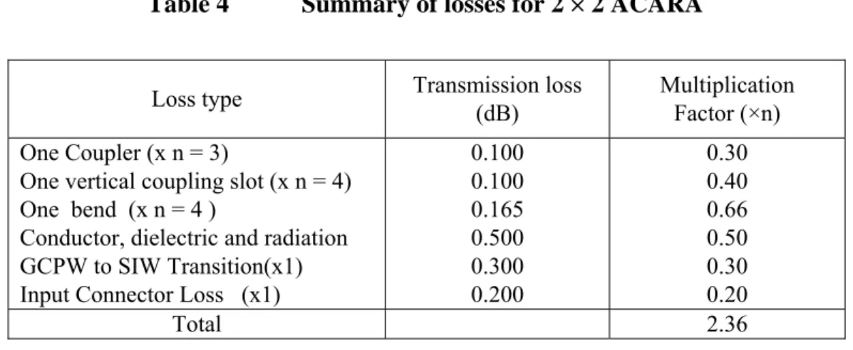
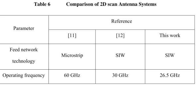
Table 1 Antenna physical parameters ... 17 Table 2 Comparison of rod antennas within substrate integrated circuits (SICs) family ... 22 Table 3 Theoretical Phase difference of Butler Matrix ... 66 Table 4 Summary of losses for 2 × 2 ACARA... 74 Table 5 Performance highlights of high-efficiency 2-D scan antenna array system ... 74 Table 6 Comparison of 2D scan Antenna Systems ... 76
LIST OF ACRONYMS AND ABBREVIATIONS 1-D One-Dimensional
2-D Two-Dimensional
3-D Three-Dimensional
ALSTA Antipodal Linearly Tapered Slot Antenna
AR Axial Ratio
BFN Beam Forming Network CR Cognitive Radio
CBCPW Conductor-Backed Co-Planar Waveguide CPW Coplanar Waveguide
CP Circular Polarization DCP Dual Circular Polarization DLP Dual Linear Polarization
EIRP Equivalent Isotropic Radiated Power HFSS High Frequency Structure Simulator
HMSIW Half Mode Substrate Integrated Waveguide LP Linear Polarization
LWA Leaky Wave Antenna MBA Multi Beam Antenna
MMICs Microwave Monolithic Integrated Circuits MPT Microwave Power Transmission
Mm-wave Millimeter-wave PCB Printed Circuits Board
SIW Substrate Integrated Waveguide SICs Substrate Integrated Circuits
SINRD Substrate Integrated Non-Radiative Dielectric Guide SIIG Substrate Integrated Image Guide
TE Transverse Electric
frequency ranges. The 60-GHz frequency band can be employed to realize the next-generation wireless high-speed communication system that is capable of handling data rates of multiple gigabits per second. The unlicensed band of 7 GHz at 60 GHz, for example, is useful and attractive for establishing high-speed wireless personnel area network (W-PAN) with a speed of at least 7 Gbps [1]. Still, in order to obtain a mm-wave link-budget that is required for wireless gigabit-per-second communication, antenna arrays are needed that should have sufficient gain and support beam-forming. The development of antenna arrays that can maintain high gain and high radiation efficiency is much anticipated for future 5G cellular communication systems and beyond. Moreover, antenna array and RF front-end should be integrated into a low-cost system on substrate that can be realized with a standard production process. The high permittivity of silicon would limit the antenna performance in terms of radiation and bandwidth. Nevertheless, the antenna designed on such a high permittivity can readily be integrated with the other silicon based platforms. The use of current wireless frequency bands limits further evolvement to higher data rates and shorter distances for two main reasons. First, the bandwidth available for these systems are limited that fundamentally limits the achievable data rate. Second, radiofrequency interference limits the operation of parallel systems within a limited range of each other. Mm-wave communication system can overcome these two hurdles. However, related link budget analysis demands for antenna arrays that have high gain and high aperture efficiency. Also, antenna arrays with multiple polarization signatures may be used to double the system data rate capability.
(a)
(c)
(d)
Figure.1.1 (a) Typical base station antenna architecture of cellular communication, (b) Indoor application of ultra-high-speed short range communication system, simplified block diagram of a radar sensor using (c) single circular, (d) dual circular polarization antenna to detect human heart beat and respiration rates.
Mm-wave base station antenna architecture is shown in Figure 1.1a. The typical antenna configuration in a cellular communication can be linear, planar, non-planar and conformal shape. In addition, beam steering capability of the base station antenna minimizes interference between adjacent users and reduces power consumption. The application of mm-wave frequency for short range ultra-high-speed communication is show in Figure 1.1b. In addition antenna with single linear and dual circular polarization characteristics are widely being used for numerous applications including radar sensors, passive imaging, energy harvesting and cognitive radio systems. The simplified block diagram of a radar transceiver using single LP antenna and CP antenna is shown in Figure. 1.1c, d. The radar with CP antenna can detect chest and heart displacement irrespective of the patient position [2]-[4]. The sensor can always detect amplitude
Figure. 1.2. Microwave power transmission (MPT) system with phase steered microwave beam on the transmission side and rectenna with high gain CP array on the receiving side. The phased array system and antenna array are using the SIW feeding network technology.
variations even the polarization of patient is not matched with the transmitting antenna. To satisfy front-end requirements of these systems, different techniques have been proposed to obtain circular polarization at mm-wave frequency.
CP purity, gain and pattern bandwidth. In the case of energy harvesting applications, CP antenna connected to rectifier is generally expected to covert RF to DC power independent of source polarization [7]. The received DC voltage is maximum and constant for CP over linearly polarized (LP) rectenna configuration.
The 60 GHz frequency band as one special mm-wave hotspot can be employed to realize the next-generation wireless short-haul high-speed communication link between inter-satellite systems [8]-[9]. The shorter wavelengths of electromagnetic waves at 60 GHz (5 mm or 0.2 inch wavelength) interact with oxygen molecules and absorbs the radiated energy. In the higher altitudes (above 43,000 kms) where there is no oxygen, 60 GHz band can offer longer communication link [8], free from electromagnetic interferences from earth over the same band. Polarization diversity antennas can transport double the data rate and offer greater flexibility in terms of size and cost of satellite antennas. For this purpose, high gain DLP antenna array is proposed and experimentally validated in this work.
The application of 1-D scan phased array antenna and high efficiency antenna array is explained using an example of microwave power transmission (MPT) system. As illustrated in Figure. 1.2, a typical MPT system consists of a phased array antenna on the transmitting side and a rectenna array on the receiving side. In the development of an efficient MPT system, antenna plays a vital role in focusing the radiating beam in a specific direction. MPT over mm-wave frequency range has been under investigation from many years [10]. General architecture of MPT consists of signal generator, power amplifier and antenna array or phase steered antenna array in the back-end. Antenna array will be able to transmit the power in only one direction and antenna array combined with phased array techniques results in multiple simultaneous directional beams. High-efficiency phased array systems were used to transmit power in multiple directions [11-13].
The choice of a mm-wave frequency range has advantages in terms of shorter wavelength and smaller antenna aperture size. However, the path losses between the transmitting and receiving antennas also increase with the operating frequency. In this case, high-gain antenna array should be designed to satisfy all requirements of mm-wave power-budget. In [14], an antenna synthesis was developed for dedicated wireless MPT and it demonstrated the maximum beam efficiency capability of the circular and rectangular planar arrays.
In addition to the typical application mentioned above, electronically steerable millimeter-wave antenna systems with 2-D scan capability have found numerous applications including radar, high-data rate communication systems, synthetic vision schemes for weapon detection and automotive collision avoidance systems [84], and cognitive radio [16]-[19]. These systems require a high-speed elevation and azimuth two-dimensional (2-D) scanning of the radiation beam to increase the performance in term of capacity, precision (resolution) and to reduce the number of the system building blocks.
First technique of 2-D scan phased array antenna utilizing phase-controlled BFN for azimuth plane scanning, and frequency controlled leaky wave sources for elevation plane scanning is demonstrated in [20]. However, many antenna front-end applications require a fixed outgoing beam in the operating frequency range. Second technique of 2-D scan phased array system utilizing phase only steered antenna system in elevation and azimuth have been studied in [21]-[24].
The 2-D scanning can be enabled in planar array by the use of phase shifters [25] or a switching beam (Butler matrix or lens-enabled techniques) which can be stacked or (volumetric) multiple-beam-forming lens as proposed in [26]. To enable a continuous scanning, the electronically steered antenna array generally are complex with a prohibitively high cost because of a large number of phase shifters involved in the system design and their considerable RF losses [27]-[30]. This is in particular true for mm-wave systems.
The concept of substrate integrated waveguide (SIW) technology offers various advantages over the conventional microstrip technology and metallic hollow waveguide. The passive beamforming techniques are mainly fixed beamforming techniques, where the numbers of output beamforming states are limited and the adaptive steering of beam can be obtained by the integration of the active components on the same system but the power distribution network adds the extra complexity to
to implement low profile beam forming network and easy to integrate along with the active components. At millimeter-wave (mm-wave) frequency, the selection of substrate integrated waveguide (SIW) in the design and development of a beam forming network topology has proven to be excellent [31]. The SIW feeding antenna arrays were realized on a silicon substrate to implement system on chip [32].
For certain applications, operating frequency should be kept constant, while the phase gradient is varied to steer the beam in elevation and azimuth simultaneously. 1-D scan system can have phase-controlled beams only in one direction where a linear phase gradient is varied along the array input contour. A beamforming network (BFN) driven linear array involves more freedom, which can be fed from an edge of array. In 2-D scan systems feeding planar arrays, phase-controlled beams are scanning in azimuth and elevation planes. The selection of a beam forming network is, nevertheless, critical in such 2-D scan systems because of the phase gradients varied along the two directions.
In this PhD thesis, phase only steered 2-D scan antenna system technique is proposed and validated at Ka-band frequency range. Such two-dimensional (2-D) scanning phased array antenna with low-cost, high-performance are highly in demand for high data-rate wireless radio links, and mm-wave imaging applications[33]-[36]. The performance of a 2-D beam-forming antenna system depends on the design of its beam-forming network (BFN) to produce constant beam direction angle θ0, beam shape and low side lobe level. Various BFN topologies to feed 1-D linear array were summarized in [87]. In 1-D beam-forming systems, the antenna placement allows to place the BFN and an array in the same plane. In 2-D beam-forming systems, phase gradient between two elements is different in horizontal and vertical directions which impose a strict requirement on the design of the BFN.
The metallic waveguide fed microstrip array has been proposed in [88] to alleviate the radiation loss problem of the microstrip feed network. The SIW fed planar microstrip array has also been proposed in [39] to overcome the limitations of conventional metallic waveguide, where a higher radiation efficiency of 79% was obtained. Nevertheless, the feed network and patch array were integrated onto the same layer, the spurious radiation from the feed network was thus not completely suppressed. The SIW cavity-backed 2 × 2 antenna arrays have been proposed to enhance the radiation efficiency up to 70% in [40] and impedance bandwidth up to 11.7% in [41]. The standing-wave SIW fed aperture-coupled microstrip array has been proposed in [42] and achieved an impedance bandwidth up to 22% at 60 GHz. The previously proposed SIW fed array applications were generally limited to only one fixed beam direction [38]-[42]. Planar and non-planar forms of various beamforming matrices like Butler, Blass and Nolen matrices were already studied in SIW technology to scan one dimensional (1-D) linear array. Recently, a 2-D scanning of planar 2 × 4 array employing a planar switched beam network that consists of two 4 × 4 Butler matrices and four hybrid couplers using the microstrip technology has been proposed for 60-GHz radio applications [91]. The loss of BFN in combination with array decreases the total radiation efficiency. The SIW based 2-D scan beam forming network has been studied and developed in [92], where single resonant slot antenna has narrow bandwidth and low radiation efficiency, and its applications are limited for feeding the 2 × 2 antenna array only.
As shown in Figure. 1.3, the basic architecture for a traditional electronically scanned array consists of transmit and receive components, a power dividing network, a phase shifting network, and an array of antennas. Phased arrays can be classified as either active or passive category. Passive arrays make use of a central transmitter and receiver, and they are able to apply a progressive phase difference to each antenna element. The passive beam-forming can be obtained by using the fixed beam forming techniques such as Butler matrix, where a better control of the radiated beams can be obtained by increasing the number of inputs to the butler matrix. With respect to active arrays, there is an individual transmit/receive module (TRM) at each antenna element that is comprised of an amplifier for high-power transmission, an amplifier for low-noise reception, and a phase shifter device.
Figure. 1.3.Beam forming network (BFN) feeding conformal array for upper hemisphere coverage, where θ is the main beam steering angle, Δθ is the required phase shift, N=the number of beam ports.
The passive beamforming techniques are mainly fixed beamforming techniques, where the numbers of output beamforming states are limited and the adaptive steering of beam can be obtained by the integration of the active components on the same system but the power distribution network adds the extra complexity to the system.
The basic operation principle of the phased array technique (using a receiver as an example) is depicted in Figure. 1.4b. The phased array receiver consists of N separate signal paths that connect to separate antennas. The desired signal from certain incident angle(s) (θ) arrives at these antennas with different time delays. In a one-dimensional antenna array receiver, the progressive time delay between two adjacent antennas is
sin /
d c
Where d is the antenna spacing and c is the speed of light. The signal received by the first antenna of a phased array receiver can be represented as
( ) ( ) cos( ( ) )
o
(a)
(b)
Figure. 1.4. (a) Principle of a phased array transmitter (b) Principle of a phased array receiver.
The time delays among the different signals paths can be compensated in the receiver so that the signals are combined coherently at the output, then the combined signal at the output can be expressed as:Sout( )t S to( ) *N, where N is the number of antenna elements.
1.1.1 Benefits of Phased Arrays
Phased arrays bring several advantages to the wireless system.
First of all, in a phased array receiver, the signals received by the multiple antennas can be added up coherently. As a result, the output signal-to noise ratio and therefore the sensitivity of the receiver can be improved by 10log10 (N) dB.
antenna transmitter. Besides, the output power of a phased array transmitter can be controlled by simply turning on or off a certain number of transmitter paths.
Thirdly, a phased array system can place nulls in undesired direction(s), which improves channel multipath profile and reduces interference to/from other systems.
Outline of thesis
This PhD thesis proposes solutions to design high-performance antenna front-end systems for obtaining single broadside beam and electronically steerable directional beam. The comprehensive work flow is organized, which covers multiple aspects of beam antenna system exploration from single broadside beam, narrow directional beam, simultaneous orthogonal directional beam, circularly polarized directional beam and then electronically steering the single beam in both azimuth and elevation simultaneously.
The second chapter of PhD thesis covers different antenna front-end systems using rod antenna as radiating element At first, planar dielectric rod antenna is proposed and used as radiating element to design high gain 45o linearly polarized antenna array. In the subsequent step, dual polarization
antenna array is designed using the rod antenna as radiating element. The planar phased array antenna using rod antenna is discussed and validated in SIW technology.
The third chapter of the PhD thesis presents and discusses the technique to obtain phase steered beams in elevation and azimuth beams simultaneously. Phase steering obtained by using analog beam forming technique is integrated under the aperture area of 2 × 2 planar array.
The fourth chapter of the thesis is dedicated to obtain circularly polarized beams in single direction and also in multiple phase steered directions. At first, single CP beam is radiated from 2 × 2 sub
array and exhibits excellent CP radiation characteristics. Dual circularly polarized antenna is designed using rod antenna as radiating element. At the end, single CP beam is phase- steered in elevation and azimuth directions simultaneously by integrating compact Butler matrix under 2 × 4 array aperture.
The fifth chapter of PhD thesis introduces and discusses phase and frequency scanning array antennas operating at E-band frequency range. Leaky wave antenna (LWA) designed in SIW technology is used as radiating element to design 2D scan phased array antennas. The frequency scanning behaviour of LWA is combined with phase scanning behaviour of Rotman lens based phase shifter to obtain multiple beam in limited scanning range. In the second part, the multi-beam antenna deploys a Butler matrix phase shifting network proposed to cover 320o scan range with
multiple beams in azimuth and 20o range in elevation simultaneously.
in the thesis are already published in the international journals and conferences. At first, dielectric rod antenna is proposed and characterized in SIW technology. The application of rod antenna in the realization of high performance antenna front-ends is discussed in detail.
60 GHz Planar Dielectric Rod Antenna
Among different types of antenna, dielectric rod antenna has widely been used due to its simplicity in architecture [45] and easy to integrate along with the milli-meter-wave integrated circuits on the single platform. The inherent wide-band nature of the rod antenna has been used for different applications including the wide bandwidth ground penetrating radar in [46]. Different techniques to design the linearly polarized antenna and antenna array were proposed in [46-51]. In [47], 60 GHz multi-layer aperture-coupled antenna array was proposed and peak gain was measured at 32 dBi with 256 radiating elements. The efficiency of array was measured to be 70%. In [48], planar SIW fed 60GHz slot array antenna was proposed and the peak gain was measured to be 23 dBi. However, the inherent narrow-band nature of the slot limits the impedance bandwidth and the series feeding method limits the pattern bandwidth. The antenna array efficiency was measured to be 68% at 60 GHz. To improve the antenna impedance and pattern bandwidth, dielectric rod antenna has been proposed in this work.
Dielectric rod antenna has been studied extensively in the literature [49-51]. Among the substrate integrate circuits (SICs) family, both substrate integrated image guide (SIIG) and integrated non-radaitive waveguide (SINRD) have been used respectively in [49] and [50] to feed dielectric rod antenna. These two families of SICs require an additional transition to communicate with the other parts of circuit. The third and well-known family member of SICs, is substrate integrated waveguide (SIW) that has also used for the design of feeding networks in [51] and to
develop high-gain dielectric rod antenna arrays. In this case, antipodal linearly tapered slot antenna (ALTSA) antenna was loaded by polyflon material to increase the gain. But, all these methods were not suitable for integration along with active circuits on a single planar platform.
2.1.1 Antenna design
The rod antenna is fabricated by using a simple printed-circuit board (PCB) process on single Rogers 3006 substrate with εr = 6.3, tan δ = 0.0012@10 GHz, and thickness = 0.635 mm.
The rod Antenna is characterized in full wave electromagnetic software HFSSv14 developed by ANSYS.
2.1.1.1 ALTSA antenna architecture
Among the end-fire radiating antenna structures, antipodal linearly tapered slot antenna (ALTSA) has widely been used in various applications thanks to its simplicity in architecture. Recently, 60 GHz ALTSA was proposed in [52] and a radiation behavior was obtained over the full band of frequencies from 55 GHz to 67 GHz. The antenna was designed on dielectric substrate (RO 4003) with εr =3.38. As substrate permittivity value increases, most of the electrical fields
will be concentered inside the dielectric region. Antenna radiation efficiency will then be decreased.
Figure. 2.3. ALTSA antenna impedance matching and gain as a function of frequency.
Figure. 2.4. ALTSA antenna simulated radiation behavior in E and H-planes at 60 GHz. 55 56 57 58 59 60 61 62 63 64 65 -40 -30 -20 -10 0 10 20 Frequency (GHz) S1 1( dB ) G ai n( dB ) -150 -100 -50 0 50 100 150 -15 -10 -5 0 5 10 Angle (o) Pe ak G ai n( dB ) E plane H plane
Figure. 2.5. Electric field strength inside the dielectric guide.
As shown in Figure. 2.1, ALTSA antenna is initially designed on dielectric substrate with εr =6.3 and all the physical parameters are given in the same Figure. Slots near H-plane of the
dielectric are corrugated to improve the cross-polarization and also the input matching of the ALTSA. All the physical parameters are optimized to obtain a good radiation pattern performance. Antenna return loss and gain as a function of frequency are shown in Figure. 2.3. Return loss of the antenna |S11| ≤ -10 dB is obtained over 16.6% of bandwidth at 60 GHz. Peak gain is better than 6 dBi over the entire desired frequency band.
As shown in Figure. 2.4, antenna gain pattern is symmetrical in E and H-planes and the half-power beam width (HPBW) in E and H-planes is of 70º. The cross-polarization value is lower than -15 dB. Peak gain of the ALTSA antenna is 7.4 dBi only. The antenna gain can be increased by changing the value of LA, but parameters TT and LM are set to be maximum possible values at this frequency on the chosen dielectric permittivity value.
2.1.1.2 Rod antenna architecture
To further enhance the gain of ALTSA antenna, dielectric rod antenna shown in Figure. 2.2 is proposed. The dielectric rod is loaded at the output and the matching at the junction is obtained by tapering the end-fire edge of the ALTSA. The output end of rod antenna is tapered to make the sharp edge and the length RM is chosen as one quarter wavelength for matching the junction discontinuities. The electric field strength is mainly concentrated inside the high permittivity dielectric of ALTSA antenna.
Table 1 Antenna physical parameters Variable Value (in mm) Variable Value (in mm) RW 1.2 TT 12º RL 10 LM 1.9 RM 5 W 0.14 L 1.6 S 1.16 LA 5.1 a 1.6
The rod antenna peak gain is as a function of rod length RL at the design frequency of 60 GHz. As the length of the rod increases, the gain also increases. Simulated Antenna radiation efficiency with and without considering losses is compared in Figure. 2.6. The ideal antenna radiation efficiency is close to 95% over the entire frequency band. When losses are taken into account for the dielectric rod, the dielectric loss tangent is set as 0.0025 for simulations at 60 GHz. The metallic sidewalls are filled up with the copper, the metallic sheet thickness is also considered to be 17 um. The antenna efficiency including all the losses is 85% at the frequency of 60 GHz.
Figure. 2.6. Simulated radiation efficiency (with and without considering metallic and dielectric losses) of the final prototype including the input transition.
2.1.1.3 Antenna cross-pol and side lobe levels
Antenna cross-pol and side lobe level as a function of substrate thickness is given in Figure. 2.7. As the substrate thickness increases, the cross pol level and side lobe levels also increase. As the thickness increases, the fields become loosely bonded within the substrate dielectric, so the polarization purity gets also reduced. For 10 mil thickness, the cross-pol value is less than -29.35 dB and the worst side lobe value is -26 dB. Finally, the antenna thickness is considered to be 25 mil for the fabricated prototype.
2.1.1.4 Measured antenna impedance bandwidth
The rod antenna is manufactured by using a simple low-cost fabrication process. The experimental prototype is shown in Figure. 2.8a. V-connector is used to measure the return loss of the antenna with Antitsu 3739C vector network analyzer. The total length of the fabricated antenna is 4λo excluding the length of feed waveguide and transition. Measured and simulated reflection coefficients are compared in Figure. 2.8b. Antenna reflection coefficient |S11| ≤ -10 dB from 55 GHz to 65 GHz. 57 58 59 60 61 62 63 64 60 70 80 90 100 Frequency (GHz) R a dai ti on ef fi ci e ncy ( in % )
With all losses Without losses
With dilelectric loss only With metallic loss only
Figure. 2.7. E-plane co-pol and cross-pol radiation pattern as a function of substrate thickness.
2.1.2 Antenna radiation pattern performance
Far field antenna pattern is measured in the MI technology anechoic chamber. Experimental prototype of the antenna is considered as receiver and the transmitting horn antenna is set a transmitter. Antenna radiation pattern is measured from 57 GHz to 64 GHz at an interval of 0.5 GHz for frequency and 1º of interval for gain patterns. Figure. 2.9, plots the normalized radiation patterns in the E and H-planes at three different frequency points 57 GHz , 60 GHz and 64 GHz. Simulated and measured results are compared and also measured cross polarization is shown in the same Figure. Both results are well in agreement and similar behavior is observed for all the remaining frequency points.
The measured gain is extracted to be 12.5 dBi at the design frequency of 60 GHz. The peak gain values are measured to be 11.5 dBi, 12.5 dBi and 12.8 dBi at 57GHz , 60 GHz and 64 GHz, respectively. Antenna HPBW is calculated to be 40º in both the E and H-plane radiation cut planes. The HPBW value of antenna is almost half when compared to the ALTSA.This is due to the loading of the ALTSA with the dielectric rod antenna. The worst side-lobe level (SLL) value is measured to be 10.5 dB lower than the maximum peak gain value. This value can be further lowered by decreasing the thickness of dielectric to 10 mil from the chosen 25 mil thickness. The measured cross polarization is lower than -17 dB at 60 GHz. The antenaa performance for different thickness is shown in Figure. 2.7. The measured gain difference or fluctuation over the bandwidth from 57 GHz to 64 GHz is less than 1.8 dBi.
-150 -100 -50 0 50 100 150 -60
(a)
(b)
Figure. 2.8. (a) Manufactured prototype of the rod antenna. (b) Simulated and measured return losses of the dielectric rod antenna.
The proposed antenna makes use of a simple transmssion line model of SICs family, exhibiting a good radation behavoir over the entire frequency band from 57 GHz to 64 GHz. Antenna radation efficiency of 85% is calculated from the measured peak gain and simulated directivity at 60 GHz . The efficiency is primarily effected by the dielectric loss of the substrate.
55 56 57
58 59
60 61 62
63 64
65
-35
-30
-25
-20
-15
-10
-5
Frequency (GHz)
S1
1
(d
B
)
Simulated
Measured
Figure. 2.9. E-plane and H-plane measured co-pol simulation (dotted), measurement (solid) and simulated cross-pol (sash-dot), measured cross-pol pattern (dash) for the rod antenna at 57 GHz, 60 GHz and 64 GHz.
In [48], 128 slot antennas were contributing to the gain of 22 dB . Also, slot antena has inherent narrowband nature When compared with SIC family of the rod antennas developed in [49]-[50] , the proposed antenna is using SIW feed type instead of SIIG or SINRD. SIW feed structre was proposed in [51], but dilelectric loading of the ALTSA makes antenna non-planar and relatively complicated to manufacture. Antenna developed in [52], was a corrugated ALTSA
-90 -60 -30 0 30 60 90 -30 -20 -10 0 Angle (o) N o rm a liz e d g a in (d B ) H plane at 60GHz -90 -60 -30 0 30 60 90 -30 -20 -10 0 Angle (o) N o rm a li z ed ga in (d B) E plane at 60GHz -90 -60 -30 0 30 60 90 -30 -25 -20 -15 -10 -5 0 Angle (o) No rm a li z ed ga in (d B ) H plane 64GHz -90 -60 -30 0 30 60 90 -30 -20 -10 0 Angle (o) No rm al iz ed gai n (d B ) E plane at64GHz
but prototype was printed on a substrate permitivity vlaue of 3.3. Antenna physical size will not allow to implement antenna arrays with different polarization signatures.
Table 2 Comparison of rod antennas within substrate integrated circuits (SICs) family
SIIG SINRD guide SIW
Fundamental mode TE11 LSM10 and/or LSE10 TE10
Transition design Uneasy to integrate with
microstrip and CPW structures
Uneasy to integrate with microstrip and CPW
structures
Easy to integrate with microstrip and CPW
structures Cut-off frequency
dependence
Substrate thickness Substrate thickness and
dielectric width
Waveguide width only
Useful for frequency range
Limited lower frequency use for because of unacceptable leakage and radiation at discontinuities
For W-band and beyond From low GHz
applications and above
Fabrication complexity
Moderate Limitation on substrate
thickness
Easy
Bandwidth of fundamental mode
< 20% < 20% ≤ 50%
Remarks Limited use because SIIG open
waveguide structure contributes to radiation loss.
Limited use because SINRD fundamental mode bandwidth may be narrow.
Widely used
45
olinearly polarized high gain antenna array for 60 GHz radio
In this section, the dielectric rod antenna is used as raiding element to implement high gain antenna array at 60 GHz frequency. Millimeter-wave antenna arrays are widely studied and developed for short-range communications, automotive radar, sensing and imaging systems.
achieved 15% of bandwidth in [57]. The solution proposed in [58] utilizes a narrow wall coupling to excite the slots etched on the top ground plane of SIW cavity. Antenna has achieved 12.6% of impedance bandwidth with 12 dBi peak gain. Multi-layer stacked Yagi-antenna with a small footprint was proposed in [59], and achieved 10.5% of impedance bandwidth with 18 dBi gain at 60 GHz. At 35 GHz, 3-D antenna array proposed in [60], has a gain of 27 dBi with 128 radiating elements.
Low temperature co-fired ceramic (LTCC) technology has been used to implement broadband high gain antennas [53]. In the dielectric rod antenna radiated beam peak gain is a function of rod length. To implement high gain and high efficiency antenna arrays, SIW-fed rod antenna has been proposed in [61] and [62]. SIW transmission line has low-loss nature at millimeter-wave frequencies due to perfect shielding nature. Therefore, low-cost antenna with high gain is studied and developed in this work.
The millimeter-wave interconnects have been mostly used for traditional transmission lines such as microstrip, co-planar wave guide and planar substrate integrated waveguide only. Among the existing techniques, wire-bonding method is the most common way to connect different transmission lines [63]. However, a significant parasitic effect of the wire bonding method not only limits the bandwidth but also contributes to the undesired radiation loss. To mitigate the radiation loss, planar interconnects were proposed in SIW technology for realizing non-planar magic T and dual polarization antenna array in [60] and [61].
In this work, a 45o LP planar array utilizing non-planar interconnect and SIW fed rod antennas
is proposed to construct high gain antenna array at 60 GHz frequency band. Array occupies a total volume of 2.8 λ × 3.2 λ × 5.1 λ with an average peak gain of 17.5 dBi over 8.3% of pattern bandwidth.
2.2.1 3-D Antenna array design
Antenna prototype is simulated in Ansoft HFSS software and fabricated on Rogers’s 3006 substrate with 10 mil dielectric thickness. Antenna and feeding network are designed on dielectric substrate with εr =6.3 and tanδ=0.003.
2.2.2 Vertical InterConnect
A vertical interconnect operating in an upper Ka-band over 14% and 28.5% of bandwidth (with |S11|≤ -15 dB) at 35GHz was respectively proposed in [60] and [61]. The slot etched on a broad wall waveguide is narrow band with only 4% at the design frequency. The equivalent circuit is represented with shunt admittance. As explained in [8], slot is replaced by a waveguide so that bandwidth of transition is increased to 11.3%. Feed network shown in Figure. 2.10a, makes use of a vertical interconnect operating at 60 GHz. The feed part consists of slot placed at a distance
Dsh= λg/4 from shorted end of the wall, so that maximum electric field is excited in center of the slot. The parameter Dsh controls bandwidth and input impedance of the interconnect. The vertical waveguide is connected to feed guide using this slot. The power is being transferred to vertical waveguide from input waveguide. Input port 1 is placed on the feed guide and output port 2 is placed on the vertical guide. The foot print of the vertical waveguide is fit within the feed guide width. Impedance matching bandwidth is improved by selecting vertical guide width S is less than feed guide width W. The field is coupling smoothly from horizontal guide to the vertical guide without any reflections coming back to input port. As shown in Figure. 2.10b, simulated magnitude of reflection coefficient (with |S11| ≤ -20) without input transitions is covering the frequency band from 57 GHz to 63 GHz. The design and fabrication complexity has been reduced when compared to the technique proposed in [60]. The proposed vertical interconnect is used to connect feeding network and antenna elements. The Rod antenna shown in Figure. 2.11, is used radiating element to design high gain antenna array at 60 GHz frequency range. The antenna element is experimentally validated in the previous section.
(a)
(b)
Figure. 2.10. 45ᵒ rotated vertical interconnect (a) architecture (where Dsh=1.92 mm, S=1.1 mm,
Wvia=0.2 mm), (b) performance. 55 57 59 61 63 65 -40 -30 -20 -10 0 Frequency (GHz) S p a ra me te rs (d B ) S11 S21