UNIVERSITÉ DE MONTRÉAL
MILLIMETER-WAVE SUBSTRATE INTEGRATED WAVEGUIDE ANTENNA
AND FRONT-END TECHNIQUES FOR GIGABYTE POINT-TO-POINT
WIRELESS SERVICES
NASSER GHASSEMI
DÉPARTEMENT DE GÉNIE ÉLECTRIQUE ÉCOLE POLYTECHNIQUE DE MONTRÉAL
THÈSE PRÉSENTÉE EN VUE DE L’OBTENTION DU DIPLÔME DE PHILOSOPHIAE DOCTOR
(GÉNIE ÉLECTRIQUE ) DÉCEMBRE 2013
UNIVERSITÉ DE MONTRÉAL
ÉCOLE POLYTECHNIQUE DE MONTRÉAL
Cette thèse intitulée:
MILLIMETER-WAVE SUBSTRATE INTEGRATED WAVEGUIDE ANTENNA AND FRONT-END TECHNIQUES FOR GIGABYTE POINT-TO-POINT WIRELESS SERVICES
présentée par : GHASSEMI Nasser
en vue de l’obtention du diplôme de : Philosophiæ Doctor a été dûment acceptée par le jury d’examen constitué de :
M. LAURIN Jean-Jacques, P h.D., président
M. WU Ke, Ph.D., membre et directeur de recherche M. CALOZ Christophe, Ph.D., membre
To my parents, To my love Zeynab
ACKNOWLEDGMENT
First of all, I would like to express my gratitude to my PhD advisor Prof. Ke Wu, who offered me support whenever I needed it. His passion for research, his persistence, and his innovative ideas gave me the drive and the motivation to explore new frontiers and to accomplish this thesis. I would also like to thank all the personnel at the Poly-Grames Research Center when I studied in Canada, in particular Mr. Jules Gauthier, Mr. Traian Antonescu, Mr. Maxime Thibault, and Mr. Steve Dubé, whose technical assistance was essential for the realization of the prototypes. A special thank is extended to Mrs. Ginette Desparois and Mrs. Nathalie Lévesque for guiding me through the administration and to Mr. Jean-Sébastien Décarie for assistance with computer trouble.
I am also indebted to my student colleagues and friends for all the professional and personal advice, and to everybody who contributed directly or indirectly to this thesis especially. I would like to thank Simon Couture for his help to translate the abstract to French.
I would also like to thank all my teachers and professors at y master, bachelor and high school. A special thank is extended to Prof. Rashed Mohassel, Prof. Moradi, Prof. Sh. Mohanna, Prof. F. Mohanna, Prof. Arzaghi, Prof. Zarifkar, and Prof. Samiei.
A special thank goes to the members of the examination jury, who took their time to read the thesis and provided very valuable comments.
Lastly, and most importantly, I would like to thank my parents. They bore me, raised me, supported me, taught me, and loved me. I would like to express my deepest gratitude to my wife for her love, encouragement and support on short and long distance. To them I dedicate this thesis.
RÉSUMÉ
La relativement faible absorption atmosphérique dans les bandes de fréquences E et W a permis le développement de nombreuses applications sans-fil. Les bandes de fréquences de 71-76 GHz, 81-86 GHz et 94.1-97 GHz sont toutes assignées au spectre de communication sans-fil gigabyte par la Federal Communication Commission (FCC) des États-Unis. Lorsque la fréquence augmente vers la région des ondes millimétriques, l’efficacité et la qualité des lignes micro-ruban sont affectées par de sérieuses pertes de transmission et par l’interférence inter-signaux. D’un autre côté, la technologie des guides d’ondes classique est demeurée populaire pour la conception de systèmes haute perfomance dans la bande E/W. Cependant, cette technologie n’est pas appropriée pour une production à grande échelle et à faible coût à cause de sa structure encombrante et coûteuse. De plus, la structure non-planaire des guide d’ondes rend difficile la connection à des composantes planaires actives ainsi qu’à d’autres lignes planaires telles que les lignes micro-ruban et les guides d’ondes coplanaires (CPW). Afin de remédier à ce problème, les circuits intégrés aux substrats (SIC) ont été proposés comme une solution à faible coût, à efficacité élevée, planaire et intégrée au substrat pour des applications à hautes-fréquences. Les guides d’ondes intégrés aux substrats (SIW), faisant partie de la famille des SIC, possède non seulement les avantages des guides d’ondes rectangulaires mais aussi d’autres bénéfices comme un faible coût, une petite taille, un poids léger et la facilité de fabrication par les techniques de fabrication des PCB ou d’autres techniques. Dans cette thèse, nous élargissons la recherche sur les SIW en proposant et développant une variété d’antennes innovatrices, de réseaux d’antennes et de composantes passives millimétriques qui sont appliqués à la conception et à la démonstration de réseaux d’antennes intégrés et d’étages d’entrée de systèmes de communication en bande E/W.
Les contributions scientifiques principales du présent travail peuvent être résumées comme suit: z Un réseau d’antenne 4x4 utilisant la technologie des guides d’ondes intégrés au substrat
(SIW) pour la conception de son réseau d’alimentation est proposé et démontré. Des fentes longitudinales gravées sur la surface métallique du dessus du SIW sont utilisées pour alimenter les éléments du réseau d’antennes. Des cubes composés d’un matériau diélectrique à faible permittivité sont placés au-dessus de chaque réseau d’antenne 1x4 afin d’augmenter le gain des antennes patch. La largeur de bande de deux réseaux
d’antennes 4x4 est d’environ 7.5 GHz (94.2-101.8 GHz) avec un gain de 19 dBi.
z La conception d’une antenne planaire basée sur une tige diélectrique est proposée et étudiée. L’antenne est alimentée par un guide d’ondes diélectrique non rayonnant intégré au substrat (SINRD). Cette antenne présente plusieurs caractéristiques intéressantes telles qu’une grande largeur de bande (94-104 GHz), un gain relativement élevé et stable, l’utilisation d’un substrat à permittivité élevée et un rayonnement parallèle au substrat guidé par celui-ci.
z Une antenne à guide d’onde co-planaire (CPW) en forme de spirale, compacte, uni planaire, à polarisation circulaire est étudiée théoriquement et expérimentalement pour des applications à large bande. L’antenne est alimentée directement par un CPW de 50 Ω par le côté extérieur de la spirale de sorte qu’un balun d’adaptation n’est pas requis. Cette alimentation permet la capacité d’obtenir un réseau planaire d’antennes spirales. Cette antenne spirale est avantageuse à cause de sa structure uni planaire facile à fabriquer aux fréquences d’ondes millimétriques.
z Un antenne cornet pyramidale dans la bande W composée de circuits imprimés (PCB) multi-couches à faible coût est développée et démontre une grande largeur de bande couvrant 71-76 GHz, 81-86 GHz et 94.1-97 GHz. L’antenne cornet proposée a aussi l’avantage d’avoir un rayonnement dans la direction perpendiculaire au substrat et d’utiliser le SIW pour son alimentation. Des fentes transversales sur la surface métallique du dessus à la fin du SIW sont déployées afin d’alimenter l’antenne cornet. Des vias métallisés sont utilisés pour réaliser les murs du cornet.
z Une antenne à fentes de type antipode, à rétrécissement linéaire et chargée par un matériau diélectrique (ALTSA) est étudiée. Utilisant le concept du cornet alimenté par un SIW, cette antenne planaire chargée par un matériau diélectrique est caractérisée par un faible coût, un gain élevé et une efficacité élevée et est conçue pour des services sans-fil gigabytes à ultra large bande dans la bande E/W (71-97 GHz). Le gain mesuré d’un élément de cette antenne est 14±0.5 dBi tandis qu’une efficacité de rayonnement mesurée de 84.23% est obtenue à 80 GHz. Le gain mesuré d’un réseau 1x4 de cette antenne est 19±1 dBi.
décroît dont la bande passante couvre toute la bande E/W. Cette transition est composée d’une couche unique d’un substrat ayant une constante diélectrique élevée et dont la largeur est progressivement rétrécie qui fait la connection entre deux SIW. Grâce à sa structure basée sur un guide d’ondes, cette transition est isolée électromagnétiquement de l’extérieur et le bruit dû aux interférences est minimal.
z Un nouveau résean d’antennes patch à haute efficacité et ayant un gain élevé est réalisé pour les services sans-fil gigabyte point-à-point dans la bande E (81-86 GHz). La largeur de bande simulée et mesurée du réseau d’antenne sont de 7.2% ce qui permet de couvrir la bande de fréquence désirée de 81-86 GHz. Le gain mesuré du réseau d’antenne est 18.5 dBi et est presque constant sur la bande de fréquences d’intérêt. Une efficacité de rayonnement de 90.3 % est obtenue.
z Un système de réception intégré au substrat opérant sur la bande de fréquences de 81-86 GHz avec une grande largeur de bande qui atteint 5.5 GHz est présenté pour la première fois. L’étage d’entrée proposée intègre des composantes actives et passives dans un assemblage unique. Un substrat à faible constante diélectrique est utilisé pour fabriquer l’antenne afin d’augmenter sa largeur de bande et son gain tandis que des circuits actifs incluant un LNA, un multiplicateur et des multiplicateurs de fréquence sont montés en surface par MHMIC.
Les réseaux d’antennes sont une composante critique des systèmes sans-fil point-à-point dans la bande E/W car les antennes doivent satisfaire plusieurs critères. Les nouvelles antennes proposées ont un faible coût, une efficacité élevée, une grande largeur de bande ainsi qu’un gain élevé et stable ce qui les rend appropriées pour cette application. Différentes structures d’antennes qui rayonnent parallèlement ou perpendiculairement au substrat sont proposées et démontrées.
Les résultats de cette thèse ont déjà été acceptés et publiés dans 4 articles du journal IEEE Transactions on Antennas and Propagation, 2 lettres dans le IEEE Antennas and Wireless Propagation Letters, un article du journal IEEE Transactions on Components, Packaging and Manufacturing Technology, ainsi que d’autres articles de journaux et de conférences qui sont mentionnés à la fin de cette thèse.
ABSTRACT
The relatively low atmospheric absorption over E-band and W-band (frequency window) has been spurred many wireless applications. Frequency bands of 71-76 GHz, 81-86 GHz, and 94.1-97 GHz are all allocated by the US Federal Communication Commission (FCC) as parts of gigabyte wireless spectrum. As frequency increases to millimeter wave region, the efficiency and quality of microstrip lines suffer from serious transmission losses and signal interferences. On the other hand, classical waveguide technology has been popular in the design of high-performance millimeter-wave systems at E/W-band. However, this technology is not suitable for low-cost and mass production because of its expensive and bulky structure. In addition, the non-planar structure of waveguide makes it difficult to get connected to planar active components and other planar lines such as microstrip line and coplanar waveguide (CPW). To overcome this bottleneck problem, substrate integrated circuits (SICs) have been proposed as low-cost and high-efficient integrated planar structures for high-frequency applications. Substrate integrated waveguide (SIW), which is part of the SICs family, has manifested not only the advantages of rectangular waveguide but also other benefits such as low cost, compact size, light weight, and easy fabrication using PCB or other processing techniques. In this Ph.D. thesis, we extend the research of SIW to the proposal and development of various innovative antennas, antenna arrays and millimetre-wave passive components, which are applied to the design and demonstration of integrated antenna arrays and E/W-band front-end sub-systems.
The principal scientific contributions of this thesis work can be summarized in the following: z A 4×4 antenna array is proposed and demonstrated using substrate-integrated waveguide
(SIW) technology for the design of its feed network. Longitudinal slots etched on the SIW top metallic surface are used to drive the array antenna elements. Dielectric cubes made of low-permittivity material are placed on top of each 1×4 antenna array to increase the gain of circular patch antenna elements. Measured impedance bandwidths of two 4×4 antenna arrays are about 7.5 GHz (94.2–101.8 GHz) with 19 dBi gain.
z Design of planar dielectric rod antenna is proposed and studied, which is fed by Substrate Integrated Non-Radiative Dielectric (SINRD) waveguide. This antenna presents numerous interesting features such as broad bandwidth (94-104 GHz), relatively high and stable gain, use of high dielectric constant substrate, and substrate-oriented end-fire radiation.
z A compact, uniplanar, circularly polarized coplanar waveguide (CPW) spiral antenna is investigated theoretically and experimentally for wideband applications. The antenna is directly fed by a 50 Ω CPW from the outside edge of the spiral, thus a matching balun is not required. This feeding provides a capability of having an entire uniplanar array of spirals. This spiral antenna is desirable due to its uniplanar structure that offers easy fabrication at millimeter-wave frequency.
z W-band integrated pyramidal horn antenna made of low cost multilayer printed circuit board (PCB) process is developed and it shows a broad bandwidth covering 71-76 GHz, 81-86 GHz, and 94.1-97 GHz. The proposed horn antenna also has the advantages of radiation along the broadside to the substrate and it makes use of SIW as its feeder. Transverse slot on the top metallic surface at the end of SIW is deployed to drive the horn antenna. Metalized via holes are used to synthesize the horn walls.
z A dielectric loaded antipodal linearly tapered slot antenna (ALTSA) is studied with which the concept of SIW-fed horn is used to design a low-cost, high-gain and efficient planar dielectric-loaded antenna for ultra-wideband gigabyte wireless services at E/W-band (71-97 GHz). Measured gain of single element antenna is 14±0.5 dBi while measured radiation efficiency of 84.23% is obtained at 80 GHz. Measured gain of 1×4 array antenna is 19±1 dBi,
z Broadband transition of SIW designed on high-to-low dielectric constant substrate whose bandwidth covers the entire E/W-band. The transition has a single layer structure that consists of a tapered high dielectric constant substrate connecting two SIWs. Thanks to the waveguide-based structure of the transition, it has a self-shielded configuration, and its noise interference is minimum.
z A novel high-efficient and high-gain patch antenna array is realized for E-Band gigabyte point-to-point wireless services (81-86 GHz). Simulated and measured bandwidths of the antenna array are 7.2% that covers the desired frequency range of 81 - 86 GHz. Measured gain of the 4×4 antenna array is 18.5 dBi that is almost constant within the antenna bandwidth of interest. Measured radiation efficiency of 90.3% is obtained.
z A substrate integrated receiver system operating over the band of 81-86 GHz with a broadband up to 5.5 GHz is presented for the first time. The proposed front-end
sub-system integrates active and passive components within a single package. A substrate with low dielectric constant is used to fabricate the antenna for increasing its bandwidth and gain While actives circuits including LNA, mixer and frequency multipliers are surface-mounted using MHMIC.
Antenna array is a critical part of the E/W-band point to point wireless system demonstrations, because antenna should have several specifications to be suitable for point to point wireless system. The proposed novel antennas are low cost, high efficient, broad band, and also they have high and stable gain, which make them appropriate for this application. Different antenna structures which radiate end fire, or broadside to the substrate are proposed and demonstrated. The results of this PHD dissertation are already accepted and published as four journal papers in IEEE Transactions on Antennas and Propagation, two letters in IEEE Antennas and Wireless Propagation Letters, one journal paper in IEEE Transactions on Components, Packaging and Manufacturing Technology, and some other journal and conference paper which are mentioned in detail at the end of this thesis.
TABLE OF CONTENTS
DEDICATION... iii ACKNOWLEDGMENT ... iv RÉSUMÉ... ... v ABSTRACT... ... viii TABLE OF CONTENTS ... xiLIST OF FIGURES ... xiv
LIST OF TABLES ... xx
LIST OF ACRONYMS AND ABBREVIATIONS ... xxi
CHAPTER 1 INTRODUCTION ... 1
1.1 Background and Motivation ... 1
1.2 Outline of thesis ... 8
CHAPTER 2 COMPACT COPLANAR WAVEGUIDE SPIRAL ANTENNA WITH CIRCULAR POLARIZATION FOR WIDEBAND APPLICATIONS ... 10
2.1 Background and introduction ... 10
2.2 Antenna design ... 11
2.3 Fabrication and Measurement Results ... 16
2.4 Conclusion ... 21
CHAPTER 3 LOW-COST AND HIGH-EFFICIENT ANTENNA FOR W-BAND ... 22
3.1 Low-Cost and High-Efficient E-Band SIW Antenna Array Made of Printed Circuit Board Process ... 22
3.1.1 Overview and introduction ... 23
3.1.2 Design of 4×4 antenna arrays ... 23
3.1.3 Fabrication and measurement of 4×4 antenna arrays ... 31
3.2 Planar dielectric rod antenna for gigabyte wireless communication at E band ... 41
3.2.2 Design considerations of the antenna and the feed ... 42
3.2.3 Fabrication and Measurement of SINRD fed dielectric rod antenna ... 49
3.3 Conclusion ... 53
CHAPTER 4 WIDE-BAND AND LOW-COST ANTENNA FOR E/W-BAND (71-97 GHZ) GIGABYTE POINT TO POINT WIRELESS SERVICES ... 55
4.1 Integrated pyramidal horn antenna made of multilayer printed circuit board (PCB) process. ... 55
4.1.1 Introduction ... 56
4.1.2 Structure and design of integrated pyramidal horn antenna ... 56
4.1.3 Fabrication and measurement of the integrated pyramidal horn antenna ... 63
4.2 Planar high-gain dielectric-loaded antipodal linearly tapered slot antenna for E/W-band gigabyte point-to-point wireless services ... 67
4.2.1 Review and introduction ... 67
4.2.2 Dielectric-loaded antipodal linearly tapered slot antenna (single element) ... 68
4.2.3 1×4 planar array of dielectric loaded ALTSA antenna ... 79
4.3 Conclusion ... 84
CHAPTER 5 E-BAND BROADBAND TRANSITION OF SIW ON HIGH-TO-LOW DIELECTRIC CONSTANT SUBSTRATES ... 86
5.1 Introduction ... 86
5.2 Explanation of the transition ... 87
5.3 Fabrication and Measurement Results ... 94
5.4 Conclusion ... 96
CHAPTER 6 LOW COST, E-BAND (81-86 GHZ) RECEIVER FRONT-END, FOR GIGABYTE POINT-TO-POINT WIRELESS COMMUNICATIONS ... 97
6.2 High-efficient patch antenna array for E-Band (81-86 GHz) Gigabyte Point-to-Point
Wireless Services ... 99
6.2.1 Design of the patch antenna array ... 99
6.2.2 Fabrication and measurement results of 4×4 array of patch antennas ... 103
6.3 4 order Chebyshev SIW cavity filter ... 107
6.4 Wire-bondings, transitions and GCPW transition lines ... 110
6.5 Active components ... 114
6.6 Test setup and measurements of receiver front-end ... 116
6.7 Conclusion ... 119
CHAPTER 7 CONCLUSIONS AND FUTURE WORK ... 120
7.1 Conclusions ... 120
7.2 Future works ... 122
LIST OF FIGURES
Figure 1.1. Average atmospheric attenuation versus frequency [1]-[2]. ... 2
Figure 1.2. Applications of E/W-band gigabyte point-to-point communication (a) campus wireless backhaul [11]. ... 3
Figure 1.3. Topology of an SIW guide realized on a dielectric substrate [12]. ... 5
Figure 1.4. Effect of dielectric and metallic losses on insertion loss of one centimeter SIW on (a) 4 mils, and (b) 20 mils thickness substrate ... 8
Figure 2.1. Geometry and 3-D view (including radiation pattern) of the CPW fed spiral antenna... ... 12
Figure 2.2. Impact of the high dielectric constant (9.8) substrate thickness (T) on the front to back radiation ratio of the compact CPW spiral antenna at 14.5 GHz. ... 13
Figure 2.3. Effect of CPW line termination and thickness of the substrate (T) on the axial ratio of the compact CPW spiral antenna. ... 15
Figure 2.4. Effect of CPW line termination on the radiation efficiency...15
Figure 2.5. Micro-photograph of the fabricated compact spiral antenna using MHMIC technology; (a) top view, (b) 3-D view with test fixture, (c) 3-D view. ... 17
Figure 2.6. Measured and simulated return losses of the compact spiral antenna. ... 18
Figure 2.7. Measured and simulated gains of the compact spiral antenna. ... 19
Figure 2.8. Measured and simulated axial ratios of the compact spiral antenna. ... 19
Figure 2.9. Measured radiation pattern of the compact spiral antenna at frequencies of 12, 14 and 16 GHz... ... 20
Figure 3.1. Layout of a 1×4 antenna array (S1 = 0.1 mm, S2 = 2 mm, and D1=0.75 mm) ... 25
Figure 3.2. Layout of the 4×4 power divider and dimensions of the slots. ... 25
Figure 3.3. Gain at 97 GHz versus width W of the rectangular dielectric cube at thicknesses (S2) of 1, 1.5, 2, and 2.5 mm for a 1×4 array antenna. Note that dielectric or metallic losses are not considered in this simulation. ... 26
Figure 3.4. Radiation pattern in (a) XZ plane, (E plane), (b) YZ plane (H plane), of the 1×4 antenna array considering the effect of the rectangular dielectric cube. Solid: with dielectric rectangular cube, and dashed: without dielectric rectangular cube. ... 27
Figure 3.5. Simulated |S11| and |S21| of the T-shaped and Y-shaped junctions. ... 28
Figure 3.6. Simulated gain (a) and |S11|, (b) of the 4x4 antenna array considering the effect of the dielectric and metallic losses. ... 29
Figure 3.7. Layout of the 1×4 vertically stacked Yagi-like antenna array. ... 30
Figure 3.8. Photograph of the fabricated 4x4 antenna array with dielectric cubes; (a) top view, (b) bottom view, (c) antenna under test. ... 33
Figure 3.9. Measured and simulated reflection coefficients of the 4×4 antenna array with dielectric cubes. ... 34
Figure 3.10. Simulated and measured co-polarization and measured cross-polarization patterns in the E- and H-planes at (a) 95.25 GHz, (b) 97 GHz, (c) 98.75 GHz, and (d) 100.5 GHz. Solid: measured, dashed: simulated, and dotted: measured cross-polarization. ... 36
Figure 3.11. Photograph of the fabricated 4×4 vertically Yagi-like antenna array. ... 37
Figure 3.12. Measured and simulated |S11| of the 4×4 vertically Yagi-like antenna array. ... 38
Figure 3.13. Simulated and measured co- and cross- polarization patterns in E- and H-planes at (a) 95.25 GHz, (b) 97 GHz, (c) 98.75 GHz, and (d) 100.5 GHz. Sold: measured, dashed: simulated and dotted: measured cross-polarization. ... 40
Figure 3.14. (a) Conventional horn fed dielectric rod antenna, (b) planar SINRD guide-fed integrated dielectric rod antenna. ... 44
Figure 3.15. Top view of the simulated electric field distribution (Ansoft HFSS v.13) of the planar SINRD guide-fed dielectric rod antenna. ... 45
Figure 3.16. Influence of the length of the dielectric rod on the gain of the integrated SINRD guide-fed dielectric rod antenna. ... 46
Figure 3.17. (a) Top view and, (b) side view, of the WR10-to-SINRD guide transition, (c) 3-D view and top view of the SINR3-D guide-fed dielectric rod antenna and the WR10 to SINR3-D
guide transition... ... 47
Figure 3.18. |S11| and |S12| of the back to back WR10 to SINRD guide transition. ... 48
Figure 3.19. Photograph of the fabricated planar SINRD guide-fed dielectric rod antenna and the WR10 to SINRD guide transition. ... 50
Figure 3.20. Measured and simulated return loss of the planar SINRD guide-fed dielectric rod antenna... ... 50
Figure 3.21. Simulated radiation patterns in YZ plane (H plane), and XY plane (E plane), of the SINRD guide-fed integrated dielectric rod antenna at (a) 93 GHz, (b) 96 GHz, (c) 99 GHz, and (d) 102 GHz. Solid: measured, dashed: simulated and dotted: measured cross-polarizations... ... 52
Figure 4.1. Configuration of basic waveguide-based horn antenna and its waveguide feed. ... 57
Figure 4.2. Configuration of multilayer integrated horn antenna (a) Side view, (b) 3D view, and (c) Top view ... 58
Figure 4.3. Impact of the aperture of the antenna on (a) H plane, (b) E plane at 94 GHz. ... 60
Figure 4.4. Effect of adding the layers on gain and bandwidth characteristics of the multilayer integrated horn antenna. ... 62
Figure 4.5. Simulated radiation efficiency of the integrated horn antenna ... 63
Figure 4.6. Photograph of the fabricated antenna (a) top view, (b) side view ... 64
Figure 4.7. Simulated and measured |S11| of the integrated multilayer horn antenna ... 65
Figure 4.8. Simulated and measured gains of the integrated multilayer horn antenna ... 65
Figure 4.9. Simulated and measured E- and H-plane radiation patterns of the horn antenna at (a) 78 GHz, (b) 88 GHz, and (c) 98 GHz. ... 66
Figure 4.10. Structure of millimeter-wave (a) ALTSA antenna, (b) ALTSA with horn shaped via, (c) elliptical dielectric loaded ALTSA with horn shaped via, and (d) rectangular dielectric loaded ALTSA with horn shaped via. ... 69 Figure 4.11. Top view of simulated electric field distribution at 84 GHz (Ansoft HFSS v.13) of the ALTSA antenna with horn shaped via and (a) Elliptical, (b) rectangular dielectric loading (L2 = 5.5 mm)... ... 71 Figure 4.12. Impact of the horn shaped via and dielectric loading on the gain... .. 71 Figure 4.13. Impact of the horn shaped via and dielectric loading on the radiation pattern of ALTSA antenna at 83.5 GHz (a) YZ (H) plane (b) XY (E) plane. ... 72 Figure 4.14. Impact of length of the rectangular dielectric loading on the gain of the antenna at 74 GHz, 84 GHz, and 94 GHz. ... 73 Figure 4.15. Impact of the length of the loaded dielectric on the side lobe level, (a) E plane, and (b) H plane, at 74 GHz, 84 GHz, and 94 GHz. ... 74 Figure 4.16. Photograph of the fabricated (a) Elliptical dielectric loaded ALTSA, (b) rectangular dielectric loaded ALTSA. ... 76 Figure 4.17. Measured and simulated (a) |S11| and (b) Gain... ... 77 Figure 4.18. Simulated and measured radiation patterns of the rectangular dielectric loaded ALTSA in the E- and H-planes at (a) 75 GHz, (b) 85 GHz, and (c) 95 GHz ... 78 Figure 4.19. (a) Geometry of power divider (b) Simulated |S11| and |S21| of T-shaped and Y-shaped junctions. ...80 Figure 4.20. Photograph of the fabricated 1×4 array of rectangular dielectric loaded ALTSA... ... 81 Figure 4.21. Measured and simulated (a) |S11|, (b) Gain of 1×4 array of rectangular dielectric loaded ALTSA. ... 82 Figure 4.22. Simulated and measured radiation patterns of the rectangular dielectric loaded ALTSA in H and E planes at (a) 75 GHz, (b) 85 GHz, and (c) 95 GHz. ... 83 Figure 4.23. Measured |S12| of 28.778 mm long SIW on Rogers 6002 substrate. ... 84
Figure 5.1. Structure of the millimeter-wave broadband transition of SIW on high-to-low dielectric constant substrates with tapered transition. ... 88
Figure 5.2. Top view of the simulated electric field distribution (Ansoft HFSS v.13) of the broadband transition of SIW on high-to-low dielectric constant substrates. ... 89
Figure 5.3. Impact of (a) WR, and (b) LR on |S11| and |S21| of the transition. ... 90
Figure 5.4. Impact of the gap between the high dielectric constant substrate and the low dielectric constant substrate. ... 91
Figure 5.5. Micro-photograph of the fabricated back-to-back transition (before adding the conductor tape)... ... 95
Figure 5.6. Measurement setup of the transition ... 95
Figure 5.7. Measured and simulated |S11| and |S21| of the back-to-back transition. ... 96 Figure 6.1. (a) Block diagram, and (b) photograph, of the demonstrated E band (81-86 GHz) receiver front-end ... 98
Figure 6.2. Geometry and 3-D view of the (a) 1×4 antenna array, (b) 4×4 antenna array, and (c) power divider. ... 100
Figure 6.3. Simulated |S11| and |S21| of the T-shaped and Y-shaped junctions. ... 102
Figure 6.4. Influence of the thickness of the top dielectric layer on the gain of a 1×4 antenna array at 83 GHz. ... 102
Figure 6.5. Photograph of the fabricated 4×4 antenna array of patch antennas. ... 103
Figure 6.6. Measured and simulated impedances of the 4×4 array of patch antennas. ... 104
Figure 6.7. Simulated and measured gains of the 4x4 antenna array considering the effect of the dielectric and metallic losses. ... 105
Figure 6.8. Measured and simulated radiation efficiencies of the 4×4 array of patch antennas... ... 106
Figure 6.9. Simulated radiation pattern in XZ plane, (E plane), and YZ plane (H plane), (c.f. Figure 3.2) of the 4×4 antenna array at (a) 82.5 GHz, and (b) 84.5 GHz. Solid: measured, dashed: simulated, dotted: measured polarization, and dotted-dashed: simulated cross-polarization... ... 107
Figure 6.10. Structure of the filter and simulated electric field distribution at (a) 76 GHz, and (b) 84 GHz... ... 108
Figure 6.11. Photograph of the fabricated filter. ... 109
Figure 6.12. Simulated and measured |S11| and |S12| of the filter. ... 110
Figure 6.13. Micro-photograph of via after (a) drill by laser, and (b) sputter cupper coated. .. 111
Figure 6.14. Micro-photograph of the fabricated GCPW on Alumina substrate (a) after filling via holes and polishing the surface, (b) after gold sputtering and photolithography. ... 112
Figure 6.15. Measured |S12| of 3.78 mm length GCPW fabricated on Alumina substrate (solid), and CPW to microstrip line transition (dashed), and transition of microstrip line on high-to-low dielectric constant substrate (dotted). ... 113
Figure 6.16. Transition from SIW to microstrip, microstrip on high to low dielectric constant substrate, and Microstrip to CPW transition ... 114
Figure 6.17. Active components on Alumina Substrate ... 115
Figure 6.18. (a) Experimental setup diagram of E band (81-86 GHz) receiver sub system, (b) photograph of the measurement setup. ... 117
Figure 6.19. Spectra of the received IF signal ... 118
LIST OF TABLES
Table 3.1: Dimensions of the 4 ×4 antenna array………...………26
Table 3.2: Dimensions of the 4 ×4 Yagi-like antenna array………..……….31
Table 3.3: Dimensions of the Antenna and WR10-to-SINRD guide transition….….…………...48
Table 4.1: Dimensions of the integrated pyramidal horn antenna………..59
Table 4.2: Dimensions of the dielectric loaded ALTSA………....70
Table 4.3: Dimensions of the power divider………..81
Table 5.1: Dimensions of the transition………….……….82
Table 5.2: Dimensions of the transition for different materials (unit: mm)………...……92
Table 6.1: Dimensions of the 4×4 array of patch antennas………..……106
LIST OF ACRONYMS AND ABBREVIATIONS
2-D Two-Dimensional3-D Three-Dimensional ADS Advanced Design System AIA Active Integrated Antenna
ALSTA Antipodal Linearly Tapered Slot Antenna AM Amplitude Modulation
CAD Computer Aided Design
CBCPW Conductor-Backed Co-Planar Waveguide. CPW Coplanar Waveguide
CST-MWS Microwave Studio® (Computer Simulation Technology) DC Direct Current
EBG Electromagnetic Band Gap
EIRP Equivalent Isotropic Radiated Power FET Field-Effect Transistor
FHMSIW Folded Half Mode Substrate Integrated Waveguide FOM Figure of Merit
FSIW Folded Substrate Integrated Waveguide HB Harmonic Balance
HFSS High Frequency Structure Simulator
HMSIW Half Mode Substrate Integrated Waveguide IF Intermediate Frequency
IM3 Third-order Intermodulation IP3 Third-order Intercept Point
LNA Low Noise Amplifier LO Local Oscillator
MEMS Micro Electro Mechanical systems MICs Microwave Integrated Circuits
MMICs Microwave Monolithic Integrated Circuits MPT Microwave Power Transmission
MW Magnetic Wall PA Power Amplifier
PAE Power Added Efficiency PCB Printed Circuits Board RF Radio Frequency
SIC Substrate Integrated Circuits
SINRD Substrate Integrated Non-Radiative Dielectric Guide SIIG Substrate Integrated Image Guide
SIW Substrate Integrated Waveguide TE Transverse Electric
TEM Transverse Electric Magnetic TM Transverse Magnetic
TSA Tapered Slot Antenna TTL Transistor–Transistor Logic VCO Voltage Controlled Oscillator VNA Vector Network Analyzer
CHAPTER 1 INTRODUCTION
1.1 Background and Motivation
Operating frequencies of wireless communication systems have increased in order to assign radio access to a less crowded part of the electromagnetic spectrum and also provide a wider bandwidth for data transmission. The relatively low atmospheric absorption rate at E/W-band, 140 GHz, 220 GHz, 340 GHz, and 410 GHz (Figure 1.1) as transmission windows has spurred many applications and innovations at millimeter-wave frequencies and beyond [1]. A wide range of applications have attracted much attention from industry and academia to the exploitation of E/W-band (71-97 GHz) [3]-[4]. The E/W-band spectral window offers possibility great potential of gigabyte data wireless transmission over several kilometers in normal weather conditions [5]. Frequency bands of 71-76 GHz, 81-86 GHz (usually referred as E-band), and 94.1-97 GHz (part of W-band) are all allocated by the US Federal Communication Commission (FCC) as gigabyte wireless spectrum [3]-[4]. Over those frequency windows, the atmospheric absorption drops to less than 1dB/Km and spells out the capability of long-range gigabyte point-to-point wireless services [5]. Obviously, wide bandwidth and low atmospheric loss allow for the E/W-band implementation of high resolution and long-range radars [6], detectors, and sensors [7], which may be used in helicopter, aircraft/automobile collision avoidance radar, passive millimeter wave imaging, and radar sensors [8]-[10].
Figure 1.1. Average atmospheric attenuation versus frequency [1]-[2].
The application range over E/W-band is extensive and evolving quickly. Figure 1.2 (a) shows one of the main applications of E/W-Band frequencies is related to on-campus LAN connectivity that provides users with a flexible, fast and safe way to establish the network with fiber optic backbone access. E/W-band is also used for Wireless Backhaul services (Figure 1.2 (b)) to provide users with high speed, low cost and scalable means of increasing data and voice traffics to and from hard-to-reach cell towers or where the deployment of terrestrial fiber is not economically viable [11]. We can summarize the potential applications of E/W-band as follows [3]:
¾ Fiber backbone POP access ¾ Enterprise campus connectivity ¾ Local area network (LAN) extension ¾ Local area loop
¾ Metropolitan area network (MAN) ¾ Wide area network (WAN) access
¾ Central office bypass ¾ Wireless backhaul ¾ High definition video ¾ Storage access
(a)
(b)
Figure 1.2. Applications of E/W-band gigabyte point-to-point communication (a) campus LAN, (b) wireless backhaul [11].
Front-end technologies have been known as the critical enabling mover for the development of millimeter-wave systems and applications. In this connection, transmission line techniques have been playing the instrumental role in the development of such front-end platforms. Microstrip
lines have been used since decades for microwave applications due to their low-cost planar structures for a full scale of integration. As frequency increases to millimeter wave region, the efficiency and quality of microstrip lines suffer from serious transmission losses and signal interferences. On the other hand, classical waveguide technology has been popular in the design and development of high-performance millimeter-wave circuits and systems. However, the waveguide technology is not suitable for low-cost and mass production because of its expensive and bulky structure. In addition, the non-planar nature of waveguide without the possibility of integration makes it difficult to get connected to planar active components. To overcome this bottleneck problem, substrate integrated circuits (SICs) have been proposed as low-cost and high-efficient integrated planar structures for a wide range of high-frequency applications. Substrate integrated waveguide (SIW) that is part of SICs, presents not only the inherent advantages of rectangular waveguide but also offers other desirable benefits such as low cost, compact size, light weight, and easy fabrication using PCB or other processing techniques. Generally speaking, SIW consists of arrays of metallic via holes or slot trenches created in a planar substrate. Furthermore, SIWs can easily be connected to or integrated with microstrip and coplanar waveguides utilizing a wideband transition on the same substrate [12]-[16].
Thanks to the low-loss transmission characteristics of the non-radiative dielectric (NRD) waveguide, it has been demonstrated as a promising candidate for millimeter-wave applications. However, the fabrication and integration of NRD waveguides are generally not easy because of their mechanical tolerance and bulky geometry especially at millimeter-wave frequency. Substrate integrated non-radiative dielectric (SINRD) waveguide has been demonstrated successfully to overcome such fabrication and integration hurdles of the original NRD waveguide. SINRD guide presents a planar topology and can easily be connected to any other planar lines and active components. In the design and development of an SINRD guide, drilling an array of air holes reduces the effective permittivity of the bilateral surrounding areas of the central guiding strip, thus creating a dielectric channel of waveguide in planar substrate. The effective dielectric constant can be controlled by choosing an appropriate set of geometrical parameters of the array holes [17]-[20]. Other SICs structures are Substrate Integrated Image Guide (SIIG) [21], half-mode SIW (HMSIW) [22]-[28], folded HMSIW (FHMSIW) [29], and folded SIW (FSIW) [30]-[31], ridge SIW [32] etc. Generally, any non-planar structure can be synthesized into its planar counterpart through the concept of SICs such as substrate integrated
coaxial lines. This research work is primarily focused on novel antenna and front-end sub-system based on SIW technology for gigabyte point to point wireless communication at E/W-band.
Figure 1.3. Topology of an SIW guide realized on a dielectric substrate [12].
As Figure 1.3 suggests, placing two rows of metalized hole in substrate is used to synthesize the rectangular waveguide inside the substrate. Spacing b between the holes, diameter D of the holes, and spacing W between the two rows of metallic vias are basic physical parameters that are necessary in the design of an SIW. To reduce potential leakage loss between adjacent vias, period
b must be kept small. Because the diameter of via and the period length are interrelated to each
other, ratio D/b is considered to be more critical than the period length in the design. The SIW can no longer be regarded as a normal homogeneous waveguide, and it is in fact an artificial periodic waveguide [33]. The diameter of via may significantly affect the return loss of the waveguide section in view of its input port. Two basic design rules have been deducted of different SIW geometries [12]:
/ 5 2 g D b D λ < ≤ (1)
Propagation properties of TE10-like mode in SIW are very similar to the TE10 mode ofrectangular
SIW are the same as its equivalent rectangular waveguide. Subsequently, the width of SIW can be approximated by using the following equations [34]-[37]:
2 0.95 eff D W W b = − (2)
Equation (1)is valid for b < λ0 × εr/2 and b < 4D, where D is the diameter of the metallic holes.
For the fabrication and design of SIW structures at E/W-band, appropriate fabrication tolerance and material selection should be considered. First of all, because of small dimensions of the SIW at E/W-band, mechanical fabrication tolerance could have a significant impact on the performance of SIW circuits. Cut-off frequency of TE mode along SIW can be calculated from: 10
10 1 2 c eff f W εμ = (3)
Then, a simple calculation shows that 1 mil (25 µm) tolerance can change the cut-off frequency of an SIW on Alumina substrate (εr =9.8) by about ± 2 GHz at 63 GHz, and on Rogers/duroid 6002 substrate (εr =2.98) by ± 1 GHz. This can visibly change the operating frequency of SIW based-circuits especially filters and cavities. Cutting with laser beam, drilling and punching are three main techniques for making vias on substrates. Material characterization such as mechanical and thermal stability, rigidness, flexibility, and thickness of substrate usually determines which technique is appropriate for different substrate. The dimension of via and the width of SIW should always be measured accurately after fabrication. For the laser beam cutting, even the diameter of beam can be critically important. As an example, a laser beam with 2 mils diameter will reduce the width of SIW by 2 mils, which, according to equation (3) can change the cut-off frequency of SIW on Alumina substrate (εr =9.8) by ± 4 GHz at 63 GHz, and SIW on Rogers/duroid 6002 substrate (εr =2.98) by ± 2 GHz.
The characteristics of substrate are the other important aspect that should be accounted for in the design of SIW circuits at E/W-band. As frequency increases, dielectric constant and dielectric loss tangent of the material will generally change even though dielectric constant exhibits in a very stable manner. The first step of designing E/W-band circuits and components is measuring the dielectric constant and loss tangent of the substrate. As an example, according to equation (3),
changing the dielectric constant of the substrate from 2.98 to 2.8 can change the cut-off frequency of SIW by 2 GHz at 66 GHz. This can be critical in designing resonant structures such as antenna, filter and cavities.
As it is mentioned in [38]-[39], the characteristics of SIW components may change by changing the operating temperature of substrate, which should be considered in the related design process.
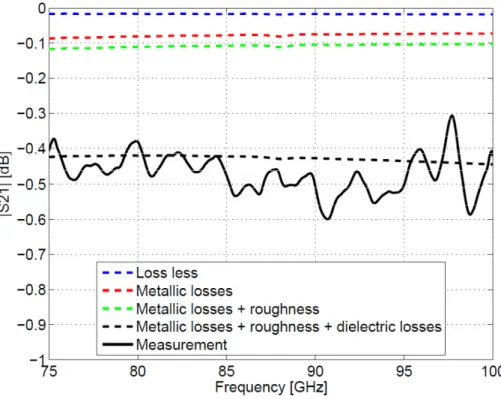
Figure 1.4 illustrates the effect of dielectric and metallic losses on insertion loss of one centimeter SIW on 4 mils and 20 mils thickness substrate. It is clear that, as the thickness of the substrate decreases metallic losses will increase and dielectric losses remains constant. Decreasing the thickness of the substrate also increases the effect of the roughness of the metal.
(b)
Figure 1.4.Effect of dielectric and metallic losses on insertion loss of one centimeter SIW on (a) 4 mils, and (b) 20 mils thickness substrate
1.2 Outline of thesis
This thesis research is concerned with the design and development of original and innovative antennas, antenna arrays, and front-end sub-systems based on SICs technology for E/W-band wireless applications such as back-haul interconnectivity. Although several SICs-based antennas, antenna arrays and beam forming networks have been recently proposed and developed, most of them have been designed and demonstrated for applications with operating frequencies lower than 40 GHz. This thesis demonstrates a number of millimeter-wave examples at E/W-bands by deploying the low-cost PCB techniques. In fact, it pushes the limiting performances and features of SIW with such techniques. The first goal of this research work is to investigate, design and demonstrate a class of novel low-cost antennas and front-end configurations for gigabyte data wireless transmission at E/W-band. The proposed antennas exhibit wide bandwidth, high gain, high efficiency and stable radiation pattern and gain within the frequency band of interest. This thesis structure is organised as follows. Chapter 2 presents a wideband CPW fed, circular
polarized spiral antenna that can be easily fabricated at high frequency. Chapter 3 presents a set of novel SIW antennas for 94-97 GHz applications. The first antenna radiates along the broadside to the substrate while the second antenna presents substrate-oriented end-fire radiation. Chapter 4 focuses on applying SIW technology to design two novel wideband antennas whose bandwidth covers the entire E/W-band of interest (71-97 GHz). In this part of the work, one antenna radiates along the broadside to the substrate, while other antenna radiates substrate-oriented end-fire. Subsequently, Chapter 5 presents a novel broadband transition of SIW on high-to-low dielectric constant substrates. Chapter 6 presents a wideband 81-86 GHz receiver front-end that is integrated into package. Finally, the last chapter concludes the thesis work by highlighting and summarizing the key concepts and contributions developed in this work as well as the future work in connection with this research project.
CHAPTER 2
COMPACT COPLANAR WAVEGUIDE
SPIRAL ANTENNA WITH CIRCULAR POLARIZATION
FOR WIDEBAND APPLICATIONS
This chapter presents a compact, uni-planar, circularly polarized, coplanar waveguide (CPW) spiral antenna for wideband applications. The antenna is directly fed by a 50 Ω CPW from the outside edge of the spiral, thus a balun for matching is not required. This feed provides the capability to have an entire uniplanar array of spirals. It is found that a thick substrate of high dielectric constant absorbs most of the radiated power and results in a unidirectional radiation pattern, which is desirable in many applications. Therefore, this antenna structure is fabricated on a substrate of high dielectric constant, resulting in miniaturization and capability for integrated system applications. The proposed topology is desirable due to its uni-planar structure which offers easy fabrication at millimeter-wave frequencies. Due to the fabrication limitation at our lab, the antenna structure is re-designed and fabricated at Ku band to prove the concept. It is experimentally verified that the proposed spiral antenna has stable radiation pattern, and its axial ratio is less than 3 dB over the frequency range of 11.4-17.5 GHz.
2.1 Background and introduction
In fact, most of the materials used for fabricating integrated circuits present relatively high dielectric constants, which provide the capability of designing antennas for integrated system applications. Spiral antennas [40] have numerous applications due to their wide bandwidth and circular polarization. Unfortunately, unless integrated with differential circuits, they generally suffer from two main disadvantages. First of all, their input impedance is not 50 Ω, and thus a wideband balun for impedance matching is required. Secondly, the central feeding leads to a thickness that incurs high fabrication cost, especially at high frequencies. Also, the central feeding makes planar array design more of a challenge.
Although different microstrip spiral antennas were studied, as frequency increases, microstrip-based configuration suffers from serious losses especially in millimeter-wave bands [14]. Coplanar waveguide is desirable due to its high efficiency at millimeter wave frequencies, and also its unbalanced and uniplanar structure. Therefore, different structures of CPW-fed spiral
antennas with external feed have been reported [41]-[43]. Although these structures provide a wide impedance bandwidth, they present circular polarization over a relatively narrow bandwidth. An externally fed three-arm spiral antenna was proposed in [44]. This antenna has a circular polarization over the frequency range of 2.3 to 3.7 GHz. Increasing the dielectric constant of the substrate decreases the dimension of the antenna but, unfortunately, also increases the axial ratio. For a substrate with dielectric constant of 6.15, the axial ratio is more than 3 dB for circular polarization. To obtain a unidirectional radiation pattern, that spiral antenna must be mounted a quarter-wave length above the ground plane, thus introducing frequency dependence [44].
Therefore, this chapter presents a compact externally fed CPW spiral antenna which is designed on an Alumina substrate of dielectric constant of 9.8. MHMIC technology is used to fabricate the spiral antenna with good processing precision. The effect of radiation absorption of thick substrates with high dielectric constant [45], [46] is used to obtain a unidirectional radiation pattern. (Note that in [45], the high dielectric constant is foremost a consequence of integration with the CMOS fabrication process.) This simple method results in a thinner antenna compared to the technique that consists of mounting the circuit a quarter-wave length above the ground plane. The proposed method also provides a stable radiation pattern for wideband applications because it is no longer dependent on wavelength. A CPW feed is desirable due to its uniplanar structure, and it does not require a balun for impedance matching; moreover, it has a high efficiency at millimeter wave frequencies. Feeding from the outside edge of the antenna provides the design capability of a uniplanar antenna array and reduces the cost of fabrication, especially at millimeter wave frequencies. Experimental results show that the antenna is circularly polarized and has a stable radiation pattern over a wide portion of the Ku-band for various radar and communications applications.
2.2 Antenna design
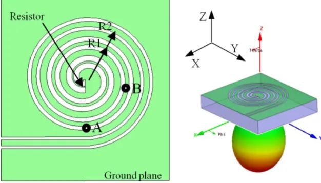
The proposed antenna structure consists of a CPW line which curls up three times. This 50 Ω CPW line is tapered linearly to its 100 Ω counterpart at the center of the antenna, and is terminated by connecting a 100 Ω resistor. Top and 3D views of the spiral antenna are shown in Figure 2.1.
The maximum radiation occurs when currents in neighboring CPW lines are in phase. To achieve the in-phase condition with respect to neighboring lines, the length of one turn must be equal to one wavelength. This means that as frequency increases, the proposed antenna will become more intensively radiating at the part more contiguous to the center. If the length of one turn is equal to one wavelength, circularly polarized radiation will also take place because the radiated electric field from points A (Ey) and B (Ex), see Figure 2.1. , will be 90 degree out of phase. This can easily be expressed mathematically by using the following equation:
)
(
1 2 0R
R
f
c
eff+
=
=
π
ε
λ
(2.1)where and are, respectively, the small and large radius of the curved line, then radius of one turn is approximately the average of and . And is the effective dielectric constant. This expression suggests that the size of the antenna has an inverse relationship with εeff .
Figure 2.1. Geometry and 3-D view (including radiation pattern) of the CPW fed spiral antenna
The radiation mechanism of the antenna is based on phase difference in two gaps, beside of the signal line of the curved CPW line, which creates common mode propagation. To increase the
radiation efficiency and decrease the power level reaching the center of the antenna, the impedance of the CPW line is increased from 50 Ω at the outside of the spiral to 100 Ω at its center. Increasing the line impedance decreases the ground plane width and puts two CPW lines closer together. This would potentially generate higher-order modes. However, our simulation results suggest that their effects are in fact negligible. These simulation results are beyond the scope of this work and thus are not shown here.
Figure 2.2. illustrates the effect of the high dielectric constant (9.8) substrate thickness (T) on the front to back radiation ratio of the Ku-band CPW spiral antenna, as analyzed by Ansoft HFSS software. Figure 2.2. suggests that by increasing the thickness of the substrate to 1.75 mm, most of the radiated energy is concentrated inside the dielectric, and a unidirectional radiation pattern is thus obtained. The effect of radiation absorption of thick substrates with high dielectric constants is illustrated in detail in [45]. Alumina is of interest for this antenna design due to its high dielectric constant (9.8) and low dielectric losses (tan δ=0.0001).
Figure 2.2. Impact of the high dielectric constant (9.8) substrate thickness (T) on the front to back radiation ratio of the compact CPW spiral antenna at 14.5 GHz.
Figure 2.3. illustrates how the axial ratio of the antenna is dependent on the thickness of the substrate and loading at the end of the CPW line. We consider four cases: with and without resistor at T=1.75 mm, and with resistor at T=1mm and 0.25 mm. As shown in Figure 2.3. , the thickness of the substrate with high dielectric constant has significant effect on the axial ratio of the spiral antenna. The best axial ratio of the antenna (1 dB at 12 GHz) is obtained by utilizing the 1.75 mm thick substrate.
Consequently, using a thick substrate with high dielectric constant decreases the axial ratio and the dimensions of the antenna; it also provides a unidirectional radiation pattern which is suitable for many applications.
Figure 2.3. also shows the effect of loading the end of the CPW line with a 100Ω resistor. Without this termination, the reflected waves increase axial ratio, because they radiate in the opposite circular polarization. The 100 Ω termination limits the reflection of waves at the end of the CPW. Terminating the CPW line has a significant effect on reducing the axial ratio although it also decreases the radiation efficiency of the antenna. The effect of loading on the radiation efficiency at different frequencies is dependent on the portion of the wave that reaches the end of the CPW line. Figure 2.4. illustrates this effect. The simulated efficiency of the loaded spiral antenna is more than 72% within the operating frequency of the antenna. Note that all dielectric, metallic, and mismatch losses have been considered in the simulations.
When designing antennas on high dielectric constant substrates, the excitation of surface waves might decrease the efficiency of the antenna and also cause side lobes. However, a comparison of radiation efficiency of the proposed compact spiral antenna in Figure 2.4. with the efficiencies of similar spiral antennas on low dielectric constant substrate, shows that the efficiencies are similar and that side lobes are absent in the simulated radiation patterns.
Figure 2.3. Effect of CPW line termination and thickness of the substrate (T) on the axial ratio of the compact CPW spiral antenna.
Figure 2.4. Effect of CPW line termination on the radiation efficiency of the compact CPW spiral antenna.
The width of the CPW signal line at the outside edge of the antenna is 0.3 mm which is tapered linearly to a 0.05 mm width at the center of the antenna in order to increase the impedance of the CPW line from 50 Ω to 100 Ω. The results show that the proposed structure can be used as a circularly polarized compact spiral antenna for wideband application in millimeter-wave frequency bands. To verify the antenna structure, a Ku-band spiral antenna was designed, simulated and measured, as shown in the next section.
2.3 Fabrication and Measurement Results
MHMIC technology, a promising technology for small scale production, is used to fabricate the proposed spiral antenna on 20 mil (0.508 mm) thick Alumina substrate. The dielectric loss tangent of this Alumina substrate is 0.0001 (at 10 GHz). A 9 mm ×7.5 mm rectangular Rogers/duroid 6010 substrate of 50 mil (1.270 mm) thickness with a dielectric constant of 10.2 is attached to the 20 mil Alumina substrate to increase the thickness of the substrate to 70 mil (1.8 mm). Note that the effect of adhesive between the layers is included in the simulation results. The spiral antenna is fabricated from a 1 µm thick gold film on the ceramic substrate (Figure 2.5. ). The 100 Ω resistor is fabricated from a thin film of Ti. Its location is shown in the inset of Figure 2.5. a. The dimensions of the resistor are 150 µm × 150µm and 20 nm in thickness. A micro-photograph of the top view of the fabricated spiral antenna, the surface resistor and a 3-D view are shown in Figure 2.5. Measured and simulated return losses of the compact spiral antenna are plotted in Figure 2.6. over the 10-20 GHz frequency range. The return loss was measured using an Anritsu 3739C vector network analyzer. The discrepancy between the simulated and measured results is attributed to the proximity of the test fixture (Anritsu 36801K right angle) to the antenna, although the test fixture was covered with a thin absorber (see Figure 2.5. b).
(a)
(b) (c)
Figure 2.5. Micro-photograph of the fabricated compact spiral antenna using MHMIC technology; (a) top view, (b) 3-D view with test fixture, (c) 3-D view.
X Y
100 Ω resistor 3.75 mm
Figure 2.6. Measured and simulated return losses of the compact spiral antenna.
Figure 2.7. shows simulated and measured gains of the compact spiral antenna over the frequency range of 11-18 GHz. In the gain measurement setup, the frequency step is 0.2 GHz. The reference plane is the YZ plane (c.f. Figure 2.1. ) for both simulations and measurements. Note that dielectric and metallic losses are included in the simulated gain of the antenna. The measured gain is determined at an elevation angle of θ = 180°. As the gain measurements suggest, the use of a high dielectric constant thick substrate allows a relatively constant gain within a wide bandwidth from 11.5-17.5 GHz. This frequency range is used for numerous applications in radars and communications.
Figure 2.8. compares the measured and simulated axial ratios of the compact spiral antenna. The magnitude at two orthogonal states is used to calculate the axial ratio of the antenna. The measured axial ratio of the antenna is less than 3.3 dB over the frequency range of 11.4-18 GHz. The discrepancy between the simulation and measurement is attributed to the effect of the test fixture that has been used to feed the antenna in our anechoic chamber.
Figure 2.7. Measured and simulated gains of the compact spiral antenna.
Figure 2.8. Measured and simulated axial ratios of the compact spiral antenna.
Measured (in YZ plane) and simulated (in both YZ and XZ planes) radiation patterns of the compact spiral antenna are shown in Figure 2.9. The measured radiation pattern of the antenna has around 10 dB front to back ratio. This suggests that most of the power is concentrated within the substrate due to the high dielectric constant, and a stable unidirectional radiation pattern is obtained over a wide bandwidth. The test fixture that has been used to feed the antenna in the
anechoic chamber has an effect on the radiation pattern, especially at θ = 100° and θ = 255°. This is because the size of the antenna is small and the antenna is too close to the test fixture, which inevitably has effects on the radiation.
Figure 2.9. Measured CP radiation pattern of the compact spiral antenna at frequencies of 12, 14 and 16 GHz.
2.4 Conclusion
A new compact spiral antenna is designed and validated both theoretically and experimentally. A CPW feed from the external edge of the antenna has been used to excite the antenna. The proposed topology is desirable due to its uniplanar structure which offers easy fabrication at millimeter-wave frequencies. The second advantage of using CPW is low radiation losses at high frequency compared to microstrip lines. This spiral antenna does not require a balun due to the unbalanced CPW feed. The use of a substrate with high dielectric constant has effectively reduced the antenna size. It is found that a thick substrate of high dielectric constant absorbs most of the radiated power and results in a unidirectional radiation pattern, which is desirable in many applications. This antenna structure is fabricated on a substrate of high dielectric constant, resulting in miniaturization and capability for integrated system applications. It is experimentally verified that the proposed spiral antenna has stable radiation pattern, and its axial ratio is less than 3 dB over the frequency range of 11.4–17.5 GHz. It is shown that using a thick substrate and terminating the CPW at the center of the spiral antenna decrease the axial ratio. Nearly constant unidirectional radiation patterns over a wide bandwidth are obtained with a thick substrate of high dielectric constant.
Next chapters will present antennas with higher gain and efficiency which are more appropriate for E band gigabyte point to point wireless communication. The goal of the following chapters is presenting some antennas with novel structures to be able to fabricate them at E band with low cost PCB fabrication process.
CHAPTER 3
LOW-COST AND HIGH-EFFICIENT
ANTENNA FOR W-BAND APPLICATIONS
This chapter presents two novel low cost, high gain and high efficient antennas for applications over W-band, e.g. 94-97 GHz in our case. The first antenna is a 4×4 antenna array that is designed on a low dielectric constant substrate and it radiates along the broadside to the substrate. The second antenna is a dielectric rod antenna designed on a high dielectric constant substrate and it features a substrate-oriented end-fire radiation.
3.1 Low-Cost and High-Efficient E-Band SIW Antenna Array Made of
Printed Circuit Board Process
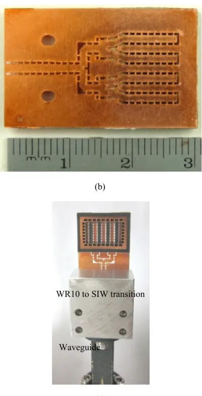
A novel class of low-cost, small-footprint and high-gain antenna arrays is presented in this section for applications over the E-band and beyond. A 4×4 antenna array is proposed and demonstrated using SIW technology for the design of its feed network and longitudinal slots on the SIW top metallic surface to drive the array antenna elements. Rectangular cubes of low-permittivity material are placed on top of each 1×4 antenna array to increase the gain of the circular patch antenna elements. This new design is compared to a second 4x4 antenna array which, instead of dielectric cubes, uses vertically stacked Yagi-like parasitic director elements to increase the gain. Measured impedance bandwidths of the two 4×4 antenna arrays are about 7.5 GHz (94.2-101.8 GHz) at 19 dBi gain level, with radiation patterns and gains of the two arrays remaining nearly constant over this bandwidth. While the fabrication effort of the new array involving dielectric cubes is significantly reduced, its measured radiation efficiency of 81 percent is slightly lower compared to 90 percent of the Yagi-like design.
3.1.1 Overview and introduction
Due to its directive radiation pattern, the Yagi antenna has been widely applied in the design of communication systems. However, it requires a boom to structurally support individual antenna elements [47]. To avoid the use of a boom, printed Yagi antennas were demonstrated in X band [48]-[49], with radiation in a plane parallel to the substrate. However, such antennas have a very large footprint. In many applications, an antenna is desired to have a broad radiation pattern in the plane perpendicular to the substrate. Therefore, an interesting approach is to use stacked director elements in a Yagi-like arrangement to increase the gain of printed antennas [50]. Later, this technique has been used in a multilayer Yagi-like microstrip antenna at 31 GHz [51], a dipole stacked Yagi antenna at 5.8 GHz [52], a dual polarized circular patch Yagi antenna at 5.8 GHz [52] and a stacked Yagi antenna at 60 GHz [53] with a very small footprint.
In this section, we present a different design technique of low-cost and high-efficiency 4×4 antenna array for E/W-band applications over the range of 94.1-97 GHz. SIW technology is used to feed the antenna elements through longitudinal slots etched on the top metallization of the SIW. The main difference compared to a similar Yagi-like array [53], which has been redesigned and is also presented for comparison, is that the original multi-layered Yagi arrangement is replaced by a dielectric block, thus significantly simplifying the fabrication process while the characteristics of the antenna array remain almost the same. Compared with previously reported millimeter-wave SIW slot antennas [54]-[56], the antenna structures proposed and developed in this section can result in higher gain, larger bandwidth and higher radiation efficiency with a more stable (less dispersive) gain within the operational bandwidth.
3.1.2 Design of 4×4 antenna arrays
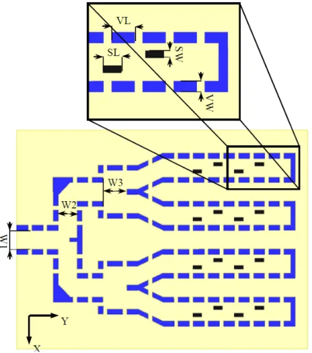
The proposed 4×4 W-band antenna array consists of four 1×4 antenna arrays as shown in Figure 3.1. Each 1×4 element has three basic layers. The bottom layer is the SIW feed network of the antenna, which is designed using a 20 mil Rogers/Duroid 6002 substrate. It is shown in Figure 3.2 for the entire 4×4 array including the one-to-four power divider. The four circular antenna elements in Figure 3.1 are fed in phase by four longitudinal, linearly polarized slots on the top metallization of the SIW. Their centers are half a wavelength apart, which amounts to
1.375 mm at the center frequency of 97 GHz. All the dimensions of the antenna are illustrated in Table 3.1. The SIWs are terminated by short circuits that are three quarter wavelengths away from the center of the last slot in order to align the slots at the peaks of the standing wave in the SIW. The design procedure is similar to the work presented in [55], and the reader is referred to [55] for further details.
The middle layer consists of circular patches of diameter D1 that are placed over slots on an Ultralam 3850 substrate of thickness S1 and dielectric constant of 2.9. The resonant frequency of the patches depends on the patch diameters and the dielectric constant of their top and bottom layers [57]. To reach the maximum gain and bandwidth, the dimension of the circular patches, the slots, and the thickness of Ultralam 3850 substrate are optimized with Ansoft HFSS.
The top layer of the 1×4 array is a rectangular dielectric cube with relative permittivity of 2.2, which is placed on top of the patches to increase the gain of the antenna. It is found that width W and thickness S2 (c.f. Figure 3.1) of this dielectric cube have a strong effect on the radiation pattern and gain of the antenna. Figure 3.3 shows the simulated gain versus width W of the dielectric rectangular cube at different thicknesses S2 of the array. It is shown that the maximum gain of 14 dBi is obtained using the dielectric rectangular cube with dimensions S2 = 2 mm and W = 1.24 mm, instead of 11 dBi without the dielectric cube. Therefore, a 3 dB gain increase is obtained through the addition of a dielectric rectangular cube. The effect of the dimension of the dielectric on the bandwidth of the antenna is negligible. Note that the mentioned simulated gain is based on IEEE gain.
Figure 3.4 shows the normalized radiation pattern of the antenna with and without the dielectric rectangular cube (W = 1.24 mm). It is observed that the antenna’s directivity is increased by adding the rectangular dielectric cube.
Simulated |S21| and |S11| of the Y- and T-shaped junctions are shown in Figure 3.5. It is noted that the T junction leads to a higher reflection coefficient than the Y junction due to the existence of 90 degree bends in this structure. In order to decrease the mutual coupling between the four 1×4 arrays, they are separated by a distance equal to 0.95λ. Due to the high directivity of the 1×4 arrays, the level of grating lobes, which results from an increase in separation between 1×4 arrays from 0.5λ to 0.95λ will be less than the side lobe level.
Figure 3.1. Layout of a 1×4 antenna array (S1 = 0.1 mm, S2 = 2 mm, and D1=0.75 mm)
Table 3.1: Dimensions of the 4 ×4 antenna array
Symbol Value (mm) Symbol Value (mm) G1 0.1 VL 0.75 G2 0.25 W 1.24 D1 0.75 W1 1.24 SW 0.24 W2 1.24 SL 0.6 W3 1.55 VW 0.254
Figure 3.3. Gain at 97 GHz versus width W of the rectangular dielectric cube at thicknesses (S2) of 1, 1.5, 2, and 2.5 mm for a 1×4 array antenna. Note that dielectric or metallic losses are not considered in this simulation.
(a)
(b)
Figure 3.4. Radiation pattern in (a) XZ plane, (E plane), (b) YZ plane (H plane), (c.f. Figure 3.1) of the 1×4 antenna array considering the effect of the rectangular dielectric cube. Solid: with dielectric rectangular cube, and dashed: without dielectric rectangular cube.
Figure 3.5. Simulated |S11| and |S21| of the T-shaped and Y-shaped junctions.
Figure 3.6 illustrates the effect of the circular patches and dielectric rectangular cube on gain (Figure 3.6a) and |S11| (Figure 3.6b) of the 4×4 antenna array. It is shown in Figure 3.6b that the bare slot array (structure of Figure 3.1 without the rectangular dielectric cube and circular patches) has one resonant frequency with 3% impedance bandwidth. By adding the circular patches on the top of the slots (structure of Figure 3.1 without the rectangular dielectric cube), the bandwidth of the structure is increased. Although adding the circular patches does not have a significant effect on the gain of the antenna, it increases the bandwidth to 7.2% (7 GHz). Figure 3.6a also shows that adding the dielectric rectangular cube on top of the patches increases the gain of the antenna array by 3.5 dB. Figure 3.6b shows that the dielectric rectangular cube does not have a significant effect on bandwidth of the antenna. For the above investigation of the effect of patches and rectangular dielectric cubes, the dimensions of the patches and slots are changed to be compatible with the structure because the resonant frequency of the circular patch depends on the dielectric constant of the top and bottom layers.
Note that for the slot array and the structure without the dielectric rectangular cube, metallic and dielectric losses are considered in the simulation. Simulated results show that including metallic loss decreases the gain of the antenna array by 0.14 dB while including dielectric loss decreases the gain by 1.18 dB; both losses do not reduce the bandwidth. To estimate the dielectric loss tangent of the substrate at 94 GHz, two different lengths of SIW are used; one to calibrate the vector analyzer, and the other to estimate the total loss. Then, HFSS
(a)
(b)
Figure 3.6. Simulated gain (a) and |S11|, (b) of the 4x4 antenna array considering the effect of the dielectric and metallic losses.
software is used to compare the simulated |S21| with the measured results. This method was used in [26] to estimate the dielectric loss tangent at 60 GHz. It is concluded that the metallic and dielectric losses do not have a significant effect on the bandwidth of the antenna array. However,
![Figure 1.3. Topology of an SIW guide realized on a dielectric substrate [12].](https://thumb-eu.123doks.com/thumbv2/123doknet/2331485.31792/27.918.224.699.255.488/figure-topology-siw-guide-realized-dielectric-substrate.webp)