To link to this article:
URL:
http://www.chalcogen.ro/1777_Essi.pdf
This is an author-deposited version published in: http://oatao.univ-toulouse.fr/
Eprints ID: 5650
To cite this version:
Essi, Marc Marie-Maurice Meledge and Yot, Pascal G. and Chevallier,
Geoffroy and Estournès, Claude and Pradel, Annie SPS-prepared targets
for sputtering deposition of phase change films. (2011) Digest Journal of
Nanomaterials and Biostructures, vol. 6 (n° 4). pp. 1777-1782. ISSN 1842
- 3582
Open Archive Toulouse Archive Ouverte (OATAO)
OATAO is an open access repository that collects the work of Toulouse researchers
and makes it freely available over the web where possible.
Any correspondence concerning this service should be sent to the repository
administrator:
[email protected]
SPS-PREPARED TARGETS FOR SPUTTERING DEPOSITION OF PHASE CHANGE FILMS
MARC MARIE-MAURICE MELEDGE ESSIa*, PASCAL G. YOTb,
GEOFFROY CHEVALLIERc, CLAUDE ESTOURNESc , ANNIE PRADELb
a
Laboratoire de Chimie des Matériaux Inorganiques, Université de Cocody, UFR-SSMT, 22 BP 582 Abidjan 22, Côte d’Ivoire
b
Institut Charles Gerhardt Montpellier, UMR 5253, Université Montpellier 2, CC 1503, Place E. Bataillon, F-34095 Montpellier cedex 05, France
c
Plateforme Nationale CNRS de Frittage Flash, Institut Carnot CIRIMAT, UMR 5085 CNRS-UPS-INP, Université Paul Sabatier, 118 route de Narbonne, 31062 Toulouse Cedex 09, France
Phase-change materials like thin films from the systems [Ge1-xPbx]Te and Ge[Te1-xSex] are
of interest for data storage. For these compositions amorphous materials can not be obtained by melt quenching. However, Suitable films can be obtained using RF sputtering. Spark plasma sintering (SPS) was used to densify the powders to obtain large targets. Synthesis conditions and characterisations of the targets are reported. Amorphous nano films were obtained using the sintered targets and characterised.
Keywords: Phase-change materials, Chalcogenides, Spark plasma sintering, RF sputtering, Thin films, Nano materials
1. Introduction
Phase-change materials are gaining increasing interest because of their use in the data storage media [1-2]. The technology is based on the reversible switching between the amorphous and crystalline phases which considerably differs in their physical properties [3]. The information is stored in the resistance state of the material. Data erasing is nothing but recrystallizing the written mark. By sensing the differences in the physical properties between the phases, data reading is possible [4, 5]. The storage concept was proposed earlier in 1968 by Ovshinsky [6]. While numerous chalcogenide phase-change alloys have been examined since few decade [7-9], M. Wuttig recently provides a clear scheme showing how to identify phase-change materials on the basis of only their stoichiometry [10]. These information are condensed in a map which describes properties with stoichiometry and locates those compositions that exhibit phase-change properties. Since this approach is predictive, well-know materials might be concerned with atomic substitutions. Therefore, substitution will enable us to extend the classification to new materials. For instance, considering GeTe binary, germanium (tellurium) could be replaced by lead (selenium) according to the substitutions rules [10, 11] giving rise to [Ge1-xPbx]Te and Ge[Te 1-xSex]. To be identified as new phase-change materials new compositions have to provide the required properties combination. As a first stage of properties investigations, our goal was to obtain amorphous material. Preparation and characterisation of suitable materials are presented in this paper.
*
2. Experimental methods
Chalcogenide alloys of Ge9PbTe10, Ge2TeSe and Ge4Te3Se were prepared by melt quenching technique. The stoichiometric amounts of elements with high purity (Sigma Aldrich®) were accurately weighed and sealed in quartz ampoules with a vacuum ~ 10-6 mbar. Silica tubes were heated in a furnace where temperature was raised at a rate of 0.1 °C.min-1 up to 950°C and kept around that temperature for 10 hours to insure the homogeneity of the samples. The obtained melts were cooled rapidly by removing the samples from the furnace and dropping to ice-cooled water. After water quenching, the bulk samples were pulverized in fine powders with homogeneous grain size of 50 µm to allow subsequent sintering.
It is well know that Spark plasma sintering makes it possible to densify materials at a lower temperature and in a shorter time compared with conventional techniques [12]. The as-prepared powder to be consolidated was then load into a cylindrical graphite die. Between the die and the powder as well as between the punch and the sample a sheet of graphitic paper was placed for easy removal. This ensemble is known as the stack. The powders were pre-compacted (applied load of § 1 ton) before introduction inside the SPS device. Consolidation was performed under vacuum (residual cell pressure <5 Pa) to avoid oxidation. A pulse configuration of 12 pulses (one pulse duration 3.3 ms) followed by two periods of zero current (6.6 ms) was used. Samples were heated through the die and punch from room temperature to 300°C with a heating rate of 50°C/min and held for 5 min at this sintering temperature. The temperature was controlled and regulated using a thermocouple put into a hole situated at the surface of the die. During the entire SPS process, a mechanical force of 5 kN was maintained through the plungers. The force was released at the end of the sintering dwell and the samples were allowed to reach the room temperature in free fall. Sintering temperature was chosen in accordance with the thermal analysis experiments showing a thermal stability of the compounds since 300°C. For comparative studies, all the samples were sintered under similar conditions. Linear shrinkage of the specimens during SPS process was continuously monitored by displacement of piston during the process.
Nano films were elaborated under Argon plasma. The deposition of the thin layers was done in a Alcatel Dion 300 set-up equipped with a turbo molecular pump, achieving a base pressure of 10-6 mbar. Films were deposited over silicon wafers. Prior to deposition, pre-sputtering was conducted using a shutter between the target and the substrate, to remove contamination on target surface. During the deposition, an Ar-gas pressure was adjusted to 10-2 mbar. Deposition was performed at room temperature with sputtering power fixed at 30 W because of the dielectric character of the chalcogenide materials. Silicon substrates were cleaned with a commercial detergent in an ultrasonic bath and rinsed in alcohol. These were cleaned one minute in diluted HF before being dried with dry air. The target to substrate distance was about 5 cm. The adherence of the membranes was checked by the classic adhesive tape test and they showed good adhesion to the substrate.
3. Results and discussions
For the studied compositions we verified that it is difficult to obtain large suitable bulk target by melt quenching (|3 cm diam.). Therefore, we use RF sputtering to get amorphous thin films. Spark plasma sintering [12] has been used to consolidate the powders in order to obtain sputtering targets. A first series of pellets were sintered in order to investigate influence of SPS process on to composition, structure and morphology. One gram of the as-prepared powders to be consolidated was load into a cylindrical graphite die of 8 mm diameter. Pellet of 8 mm in diameter and about 3mm thick were obtained. The helium densities of sintered samples were measured using an Accupy 1330 Micromeritics apparatus. The densification was calculated through the theoretical densities of raw materials and was found to be close to 97%. A CAMECA SX100 electron probe micro-analyser employing five wavelength-dispersive spectrometers was used for chemical analysis. The experiments were made with a beam intensity of 10 nA and an accelerating voltage of 20 keV. For EPMA measurements the sintered materials were cut in their middle along the pressing axis. The surface of Ge9PbTe10 sintered sample is shown in figure1 (a).
(a) (b) (c)
(d) (e) (d)
Fig. 1. Electron probe-microanalyser image of Ge9PbTe10 (a), Ge2TeSe (b) and Ge4Te3Se
(c). SEM morphology of the fracture surface of Ge9PbTe10 (d), Ge2TeSe (e) and Ge4Te3Se
(c)sintered targets.
The distribution of the phases can be easily distinguished. Some white spots randomly distribute in the matrix are observed. EPMA has shown that these white spots have a high Pb concentration and average contents of Ge, Pb and Te taken from few spots are 29.9, 19.7 and 50.05 at.% respectively. The remaining area represents Ge9PbTe10 alloy with average Ge, Pb and Te contents being 44.24, 4.85 and 50.57 at.%, very close to the stoichiometry of the starting materials (Table1). This suggests that there is an inhomogeneous distribution of lead in the sample. It is clearly evident that few phases coexist in the sintered sample. Among them, one with a composition close to the stoichiometry and a phase with high lead concentration. Concerning Ge[Te1-x Sex] alloys, we did not identify any secondary phases using electron probe micro-analyser (figures 1(b) and(c)). On the whole the data obtained by EPMA indicated that both sintered target were homogeneous. The relative amount of elements was close to the one existing in the starting materials. The average contents of Ge, Te and Se are 49.67, 38.51 and 11.51 at.% for Ge4Te3Se (Table 1). For Ge2TeSe the values were found to be 49.68, 25.8 and 24.25 at.% respectively for Ge, Te and Se (Table 1).
Table 1. Nominal compositions (Theor.), chemical compositions of sintered materials (Target) and of thin films measured by EPMA.
Ge9PbTe10 Ge4Te3Se1 Ge2TeSe
Theor. Target Film Theor. Target Film Theor. Target Film
Ge 45 44.24 43.22 50 49.67 47.54 50 49.68 50.05 Pb 5 4.85 5.18 - - - - - - Te 50 50.57 51.6 37.5 38.51 40.44 25 25.8 23.67 Se - - - 12.5 11.51 12.02 25 24.5 26.29 100 µm 100 µm 100 µm 3.33 µm 2.31 µm 2.31 µm
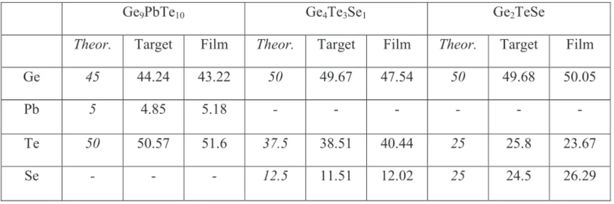
In addition to chemical analysis, microstructural and morphological characterisations of the samples have been carried out. The SEM images have been recorded with a HITACHI S-4500I scanning electron microscope operating at 15 kV. The materials obtained by SPS processes were investigated after fracture of samples. First, the SEM images (figures 1(d), (e) and (f)) were effective in obtaining dense materials. The microstructural analyses show that SPS-prepared targets result in bulks with randomly oriented grains. This result shows that during the process, in addition to the uniaxial force applied through the puncher, and additional horizontal force from the mould walls are also acting on the sample. Then, the pressure around the sample seems like a hydrostatics pressure leading to the dense target but with randomly grain orientation. Similar results are obtained using SPS technique [13, 14]. In addition, a laminar texture was observed from the fracture. On the other hand, secondary electron SEM images show that after SPS processes, the resulting samples consist of soft agglomerated pellets with sizes less than 200 nm. No pores and abnormal grains were found in all fields of view of SEM observations. X-ray diffraction measurements was carried on to identify phase formation and then to follow the structural changes under consolidation. Structural studies for sintered samples were done thanks to Seifert diffractometer equipped with a copper cathode and a backward monochromator. Range of scanned angles (2ș) was 10-80 with a step of 0.02° and exposure time of 4s. Figure 2(a) shows the XRD patterns of Ge9PbTe10 powder. Characteristic peaks of the rhombohedral GeTe were indentified and indexed with the 47-1079 JCPDS card [15, 16]. The XRD pattern of the corresponding material after SPS process is given in figure 2 (b). It is shown that sintering process led to appearance of weak peaks arising from the cubic “Altaite” phase (PbTe) indentified with the 78-1905 standard JCPDS card [16, 17]. This result is in agreement with the data obtained by EPMA measurements confirming the presence of two crystalline phases. Similar results were observed
with Ge2TeSe compounds. The starting powder was found to be a mixture of rhombohedral GeTe
and GeTeSe (JCPDS cards 39-1070) [16] crystalline phases. In addition, for the SPS-prepared target Ge2TeSe, new peaks in diffraction pattern appear. They belong to the cubic GeSe (JCPDS card 27-1154) [16]. In fact, during the SPS course heating rate and rapid densification may allow the formation of a secondary phase. At the opposite, the diffraction patterns of both powder and sintered Ge4Te3Se materials were observed to be similar and all reveal a mixture of GeTe and GeTeSe crystalline phases.
Fig. 2. Powder XRD patterns of Ge9PbTe10 samples. Starting powder (a), SPS-prepared
target (b), and GIXRD pattern obtained with the obtained thin film (c).
We have to note that above characterizations were satisfying in obtaining dense sintered materials. Consolidation by SPS process may involve significant changes of phase compositions and structures, so that the values of relative density could not show the real densification level. However, to facilitate rapid and complete switch between the amorphous and crystalline states, less heterogeneous targets have been selected for thin films elaboration.
Sputtering targets were consolidated by SPS technique using conditions determined by analysing the data recovered from the 8 mm diameter targets characterisations. 18 grams of selected samples were loaded into 26 mm inner diameter graphite dies. The temperature increased to 350°C directly at 50°C.min-1 and held for 5 min at this temperature. The pressure was applied through the plungers in two steps. First, a load of 30.6 kN was applied with a dwell time of 6 min. To complete densification, this step was followed by the application of a uniaxial force of 45.9 kN for 5 min at 350°C. The resulting targets have a cylindrical form with a height of 5 mm and a diameter of 26 mm. The densities of all targets evaluated from the masses over samples size is 98% of the theoretical densities. Subsequent deposition was carried out using RF cathodic sputtering set up. The substrate holder was neither rotated nor heated, but cooled down by water circulation. The amorphous nature of the sputtered films was investigated over the 2ș diffraction angle range of 25-47°. To increase the diffraction volume and avoid the diffraction peak from Si substrate, glancing incidence X-ray diffraction (GIXRD) was performed (PANalytical X’pert MRD). The glancing angle between X-rays and the membrane surface was 0.1°. Experiments were performed using copper X-ray tube working at 45 kV and 35 mA. A parabolic multilayer mirror was used as the primary optic and parallel plate collimator with a flat graphite monochromator was used as the secondary optic. X-ray diffraction patterns were then recorded with a measuring time of 120 s per step. As shown in Fig. 2(c), the XRD patterns presented no diffraction peak confirming the amorphous state of the layers. The obtained thin films are then suitable for further investigations in order to characterize the optical properties and writing performance of new materials. For instance, reversible light-induced crystallization might be used to involve phase change of the amorphous films [18]. The deposited thin films were observed by SEM.
(a) (b) (c)
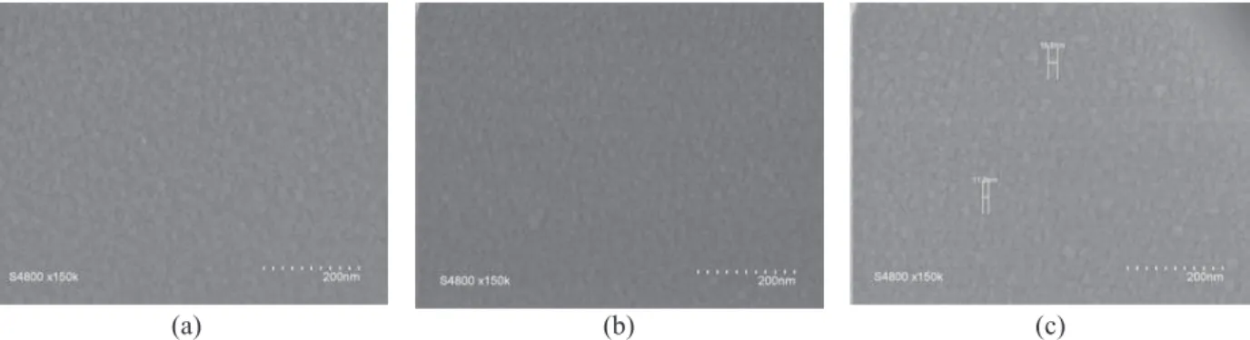
Fig. 3. SEM micrograph of thin films
The layers exhibit surface of good quality without observable defects. As can be seen in figure 3 the nanostructure shows the presence of grains that are probably due to the presence of a columnar structure perpendicular to the surface. Such morphology is often observed for films deposited by RF sputtering [19, 20]. It is shown that the average column size was approximately the same whatever the thickness, but that the columns gathered to form clusters when the thickness increased. The films thickness and roughness were determined from atomic force microscopy (AFM). For the studied compositions, the speed deposition target ranged from 2 to 3 nm.min-1. Thickness measured at different points of a sputtered film was shown to be maximum at the centre and to decrease as the point moves away from it, following a cosinusoidal law [21]. Membranes deposited under the same conditions were characterised by the same thickness at the centre. It can be noted that the roughness is different from one point of the film to another. It is maximum at the centre of the layer and decreases as the point moves away from the centre. Such a variation was expected taking into account the change in the thickness at different points of the thin films. The nature of the elements included in the film was determined by EPMA allowing simultaneously the obtaining of a good quantification of chemical composition. This analysis showed that the average contents of elements in the deposited thin films are close to that existing in bulk materials used for
target (Table 1). The compositions were also proved to be reproducible. Nano devices exhibit no significant difference in roughness according to the corresponding values 2.9, 3.1 and 2.8 nm respectively for Ge9PbTe10, Ge2TeSe and Ge4Te3Se.
4. Conclusions
Suitable sputtering targets were prepared using spark plasma sintering technique. Taking the advantages of SPS process, fully dense chalcogenide alloys were fabricated at low sintering temperature in short time cycle. Structural characterization of sintered samples indicated the presence of secondary phases which did not avoid amorphous films formation. The resulting sputtered layers were found to be homogeneous with a good surface state. The success of the elaboration of nun crystalline nano devices encourages us to establish the suitable conditions to get reversible switching between the amorphous and crystalline state. Future works, including the study of the phase change properties, will be reported elsewhere.
References
[1] J. Tomforde, S. Buller, M. Ried, W. Bensch, D. Wamwangi, M. Heidelmann, M. Wuttig, solid state science 11, 683 (2009).
[2] W. Weánic, M. Wuttig, materials today 11, 20 (2008).
[3] J.B. Wachter, K. Chrissafis, V. Petkov, C.D. Malliakas, D. Bilc, T. Kyratsi,
K.M. Paraskevopoulos, S.D. Mahanti, T. Torbrügge, H. Eckert, M.G. Kanatzidis, J. Solid State Chem. 180, 420 (2007).
[4] M. Wuttig, C. Steimer, Appl. Phys. A 87, 411 (2007). [5] M. Wuttig, N. Yamada, Nature Mater. 6, 824 (2007). [6] S. Ovshinsky, Phys. Rev. Lett. 21, 1450 (1968)
[7] E. Morales-Sanchez, E.F. Prokhorov, J. Gonzalez-Hernandez, A. Mendoza-Galvan, Thin Solid Films 471, 243 (2005).
[8] T. Zhang, Y. Cheng, Z. Song, B. Liu, S. Feng, X. Han, Z. Zhang, B. Chen, Scripta Materialia 58, 977 (2008).
[9] W. Welnic, A. Pamungkas, R. Detemple, Ch. Steimer, S. Blügel, M. Wuttig, Nat. Matters 5, 56 (2006).
[10] D. Lencer, M. Salinga, B. Grabowski, T. Hickel, J. Neugebauer, M. Wuttig, Nature Mater. 7, 972 (2008).
[11] J.R. Chelikowsky, J.C Phillips, Phys. Rev. B 17, 2453 (1978). [12] M. Tokita, J. Soc. Powder Tech. Jpn. 30, 790 (1993).
[13] J.G. Noudem, J. Eur. Ceram. Soc. 29, 2659 (2009).
[14] Y. Liu, Y. Lin, Z. Shi, C-W. Nan, Z. Shen, J. Am. Ceram. Soc. 88, 1337 (2005). [15] B. Liu, Z. Song, T. Zhang, S. Feng, B. Chen, Appl. Surf. Sci. 242, 62 (2005). [16] JCPDS cards. 47-1079 (GeTe), 78-1905 (PbTe), 39-1070 (GeTeSe), 27-1154 (GeSe). [17] L. Kungumadevi, K. Rajasekar, A. Subbarayan, R. Sathyamoorthy, Ionics 14, 63 (2008). [18] S. Kim, X.Z. Li, S. Lee, K.-H. Kim, S.-Y Lee, Ultramicroscopy 108, 1110 (2008). [19] F.O. Méar, M. Essi, P. Sistat, M.-F. Guimon, D. Gonbeau, A. Pradel, Appl. Surf. Sci. 255, 6607 (2009).
[20] F.O. Méar, M. Essi, M.-F. Guimon, A. Pradel, Chalcogen. Lett. 5, 117 (2008). [21] M. Essi, A. Pradel, Chalcogen. Lett. 8, 301 (2011).