HAL Id: hal-02862234
https://hal-univ-rennes1.archives-ouvertes.fr/hal-02862234
Submitted on 17 Jul 2020
HAL is a multi-disciplinary open access
archive for the deposit and dissemination of
sci-entific research documents, whether they are
pub-lished or not. The documents may come from
teaching and research institutions in France or
abroad, or from public or private research centers.
L’archive ouverte pluridisciplinaire HAL, est
destinée au dépôt et à la diffusion de documents
scientifiques de niveau recherche, publiés ou non,
émanant des établissements d’enseignement et de
recherche français ou étrangers, des laboratoires
publics ou privés.
Distributed under a Creative Commons Attribution| 4.0 International License
fabricated by sputtering and pulsed laser deposition
Simone Normani, Geoffrey Louvet, Emeline Baudet, Marek Bouška, Jan
Gutwirth, Florent Starecki, Jean-Louis Doualan, Yannick Ledemi, Younès
Messaddeq, Jean-Luc Adam, et al.
To cite this version:
Simone Normani, Geoffrey Louvet, Emeline Baudet, Marek Bouška, Jan Gutwirth, et al..
Compar-ative study of Er-doped Ga-Ge-Sb-S thin films fabricated by sputtering and pulsed laser deposition.
Scientific Reports, Nature Publishing Group, 2020, 10 (1), pp.7997. �10.1038/s41598-020-64092-3�.
�hal-02862234�
comparative study of er
3
+
-doped
Ga-Ge-Sb-S thin films fabricated
by sputtering and pulsed laser
deposition
Simone normani
1, Geoffrey Louvet
2,3, Emeline Baudet
1, Marek Bouška
1, Jan Gutwirth
1,
Florent Starecki
4, Jean-Louis Doualan
4, Yannick Ledemi
3, Younes Messaddeq
3,
Jean-Luc Adam
2, petr němec
1& Virginie nazabal
2,1✉
Despite the renewed interest in rare earth-doped chalcogenide glasses lying mainly in mid-infrared applications, a few comprehensive studies so far have presented the photoluminescence of amorphous chalcogenide films from visible to mid-infrared. This work reports the fabrication of luminescent quaternary sulfide thin films using radio-frequency sputtering and pulsed laser deposition, and the characterization of their chemical composition, morphology, structure, refractive index and Er3+
photoluminescence. The study of Er3+ 4i
13/2 level lifetimes enables developing suitable deposition
parameters; the dependency of composition, structural and spectroscopic properties on deposition parameters provides a way to tailor the RE-doped thin film properties. The surface roughness is very low for both deposition methods, ensuring reasonable propagation optical losses. The effects of annealing on the sulfide films spectroscopy and lifetimes were assessed. PLD appears consistent composition-wise, and largely independent of the deposition conditions, but radiofrequency magnetron sputtering seems to be more versatile, as one may tailor the film properties through deposition parameters manipulation. The luminescence via rare earth-doped chalcogenide waveguiding micro-structures might find easy-to-use applications concerning telecommunications or on-chip optical sensors for which luminescent sources or amplifiers operating at different wavelengths are required.
In recent times, the range of electromagnetic spectrum covering mid-wavelength infrared (MWIR) and long-wave infrared (LWIR), has become an appealing option for cutting-edge chemical sensing applications, due to its encompassing the excitation of fundamental vibrational transitions for many molecules, specifically in gaseous or in liquid phase1. Depicted interest in the mid-infrared range has raised the need for the development
of novel low-loss optical devices, which in turn spurs the research also in the direction of new MWIR/LWIR radiation sources and amplifiers. As of now, the main light source operating in the infrared is the quantum cas-cade laser, which provides a wide emission wavelength range beyond the near-IR2,3 and therefore represents an
important stepping stone in the advancements on this topic. Another crucial advancement is the miniaturization of sensors, which has been achieved by developing integrated optical components, allowing for compact and performant devices, and which is still a subject of research in order to optimize the means, the scale and the costs of the production.
Due to their low phonon energies and wide transmission window that extends far into the infrared region of the spectrum4–6, chalcogenide glasses doped with rare earths (RE) are essential to the development of integrated
active optical devices in the near-wave infrared (NWIR)-to-LWIR range. Moreover, thanks to their high nonlin-earities, chalcogenide glasses are particularly appealing for the development of all-optical signal processing7–9.
Amorphous chalcogenide thin films can be deposited relatively easily via radiofrequency (RF) sputter-ing10–12 and pulsed laser deposition (PLD)13, which makes it possible to obtain performant confined structures
1Department of Graphic Arts and Photophysics, Faculty of Chemical Technology, University of Pardubice, 53210,
Pardubice, Czech Republic. 2Univ Rennes, CNRS, ISCR (Institut des Sciences Chimiques de Rennes) – UMR 6226,
F-35000, Rennes, France. 3Centre d’Optique, Photonique et Laser (COPL), 2375 rue de la Terrasse, Université Laval,
Québec, Qc, Canada. 4CIMAP UMR-CNRS 6252, Université de Caen Normandie, 14050, Caen, France. ✉e-mail:
virginie.nazabal@univ-rennes1.fr
such as waveguides and resonators. In recent years, many advances have been made in the development of chalcogenide-based microstructures for in situ MWIR sensing, for instance in the medical field14 and for
vari-ous environmental applications15,16. This field of research has the aim of paving the way for the development of
easy, cheap and possibly large-scale production techniques1 for MWIR devices. Especially, erbium-doped
quater-nary chalcogenides such as Ga-Ge-Sb-S have been shown as a suitable choice for amplification and laser genera-tion17 and for sensing applications in the MWIR. If one considers erbium for RE doping, some works have to be
cited on various chalcogenide matrices like Ge10As40Se25S25:Er3+, 70Ga2S3:23La2S3:6La2O3:Er3+, As2S(Se)3:Er3+,
Ge33As12Se55:Er3+, Ga-Ge-Se:Er3+ (Ga: 3–54 at. %, Ge: 0–35 at. %, Se: 21–70 at. %), Ga5Ge20Sb10S65:Er3+ for thin
film deposition using RF sputtering method17–21, 0.15Ga
2S3–0.85GeS2:Er3+, Ge30Ga5Se64Er1, Ga5Ge20Sb10S(Se)65,
and GaLaS glass matrices deposited with PLD metod22–25, eventually (GeS
2)67(Ga2S3)33:Er3+, As2S3:Er3+
or As24S38Se38:Er3+ matrices deposited by evaporation with erbium implantation and As2S(Se)3:Er3+ and
Ge3Ga28Se70:Er3+ matrices by thermal co-evaporation26–28. Depending on the physical vapor deposition (PVD)
method and the selected composition (with gallium or without, with arsenic or without, sulfides or selenides), the results obtained are relatively disparate and difficult to compare as the parameters change from one to another chalcogenide thin film. It should be noted that relatively few publications mention results within channelled guides allowing both a relatively efficient fluorescence in propagation mode coupled with limited optical losses and a concentration of erbium sufficiently high for integrated optics, and even fewer papers show luminescence in the mid-infrared. Under optical pumping at 1.55 µm, broadband guided mid-infrared photoluminescence was recorded for the first time above 3 µm from RE doped integrated chalcogenides waveguides29. Other rare
earth-doped quaternary chalcogenide optical fibers with specific Ga-Ge-Sb-Se composition have also been suc-cessfully implemented in MWIR for gas sensing and for exploring the spectral range of LWIR using Tb3+, Dy3+
and Sm3+30–32. Given the properties of these amorphous materials, one can recognize the potential for
applica-tions of this kind of materials as both efficient sensors and laser sources, particularly in integrated optics. In this work, we show an extensive study of erbium-doped Ga-Ge-Sb-S thin films fabricated by PLD and RF sputter-ing, comparing the two PVD methods and the effects that the deposition conditions have on their composition, morphology, topography and optical properties. Erbium ion doping was chosen, although this RE is relatively ineffective in generating an emission in the mid-IR spectral range except around 2.7 μm, given a very unfavorable branching ratio to allow an emission at 4.5 μm. On the other hand, erbium allows us to follow its spectroscopic characteristics in the near infrared in sulfide thin films and thus to obtain very valuable information on the man-ufacturing process of rare earth-doped chalcogenide films devoted to infrared emission. Thanks to the knowledge of these different chemical, optical or spectroscopic characteristics put into perspective in relation to the deposi-tion condideposi-tions, the aim of this study is to obtain a detailed understanding of the advantages of one PVD method over the other, and the possibilities of adapting the properties of the chalcogenide thin films by adjusting the set manufacturing parameters.
Results and Discussion
In order to better control the manufacturing process of PLD and RF sputtered thin films of erbium-doped sulfides, as well as to better know the specific role and impact played by the two deposition techniques on the final results and characteristics, two sets of samples deposited by PLD and RF sputtering, were prepared and studied by recording their chemical composition, morphology, local structure and spectroscopy. The results of the anal-ysis are presented in the following paragraphs, showing the dependence of various properties on the deposition parameters in the range of variation studied: in principle, we will show how the thin films resulting from the PLD technique are generally insensitive to variations in these parameter sets, whereas a trend can be identified for RF sputtering method.
Chemical composition of sulfide thin films and targets.
The chemical composition of the deposited films as well as the used targets was estimated via energy dispersive X-ray spectroscopy (EDS). The results are reported in Table 1, along with the refractive index estimation from variable angle spectroscopic ellipsometry (VASE).One can see that the deposited films all share a deficiency in sulfur concentration with respect to the target composition, which is a little bit more pronounced in the PLD samples (an average of 10 at. % vs. 9 at. % for the sputtered films). Consequently, the other elements concentration is on average higher than the target’s, and in particular, the Ge and Sb concentration is sensibly larger in the PLD thin films than in the bulk, as is the Ge and Ga concentration in RF-sputtered samples. This can be understood in the case of sputtering method by difference in sputtering rate of sulfur and antimony compared to gallium and more over germanium atoms12,33. Whatever
the PVD technique used, chalcogen atoms are always deficient in composition. Less energetic, lighter, they must probably be more sensitive to the dynamic vacuum created in the chamber, to the renewal of the process gas, and consequently less deposited on the substrate than the other atoms. It should also be noted that this chalcogen defi-cit will be more or less marked from one deposition chamber to another and will depend mainly on the volume of the chamber, the position of the targets in relation to the secondary vacuum pump, the gas flow in the chamber and its aeraulic.
The chemical elements concentration was plotted as a function of the deposition parameters. The trends were then observed as a function of chamber pressure. In fact, one can see that while the sulfur deficiency is for the most part independent of the argon pressure in the case of PLD films (Fig. 1a), it follows a decreasing trend as a function of pressure in sputtered thin films whatever the RF power as it was already observed in the case of Ge-Sb-Se sputtered films12,34 (Fig. 1b,c).
Morphology, topography and refractive index of Er
3+-doped Ga-Ge-Sb-S thin films.
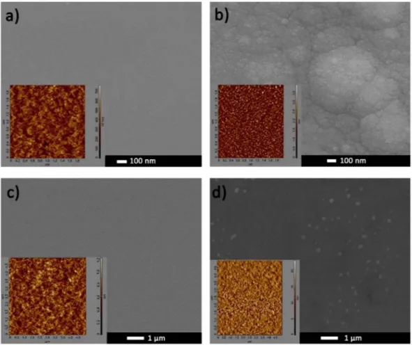
The thinVASE data. The deposition rate of PLD thin films (ranging from 18 to 63 nm/min) is consistently higher than that of sputtered samples (ranging from 3 to 18 nm/min), which is typical for PLD when compared to the RF-sputtering process of dielectric targets, even enhanced by magnetron. From the AFM and SEM measure-ments it appears that the morphology of the samples is not strongly influenced by power, energy density, nor target-to-substrate distance, and most samples show quite low root mean square surface roughness (below 0.5 ± 0.1 nm, scanned area of 5 µm × 5 µm). In addition, sputtered samples appear to have the better surface mor-phology, with generally somewhat lower roughness than PLD samples (under 0.3 ± 0.1 nm). However, as one can see in Fig. 2, samples deposited with relatively high chamber pressure have very high rough surfaces (up to more than 4 nm), which is in accordance with expectations, as the gas provides additional resistance to the extracted particles flow, therefore the deposited film homogeneity.
The refractive index difference between the films and the targets was investigated as a function of the different deposition parameters. One can see from Table 1 that the films’ refractive index is always greater than that of the bulk targets. While most parameters (energy density, RF power, target-to-substrate distance) do not show any univocal effect on refractive index, it was observed that pressure seems to play a definite role. PLD samples do not show a change in the refractive index that would follow a pronounced behavior. The refractive index of sputtered samples, instead, appears to be influenced by pressure. Figure 3 shows the variation of the sputtered thin film refractive index as a function of argon pressure in the chamber: the mismatch decreases with increasing argon
Sample
PLD Samples
p E.D. d Chemical Composition (±1 at.%) Ref. Index
mbar J/cm2 cm Real composition Δ%Ga Δ%Ge Δ%Sb Δ%S Δ1.55 µmn (±0.01)
P-1 N/A 2.4 6 Ga8Ge23Sb14S55 2 5 4 −11 0.26 P-2 N/A 2.1 6 Ga7Ge23Sb13S57 2 4 3 −9 0.19 P-3 N/A 1.7 6 Ga7Ge22Sb14S57 2 4 3 −9 0.22 P-4 N/A 2.4 8.5 Ga8Ge23Sb12S57 2 5 2 −9 0.19 P-5 5·10−4 2.4 6 Ga 8Ge23Sb14S55 2 4 4 −10 0.21 P-6 5·10−3 2.4 6 Ga8Ge23Sb14S55 2 5 4 −11 0.26 P-7 5·10−3 2.1 6 Ga 8Ge23Sb14S55 2 5 4 −11 0.25 P-8 5·10−3 1.7 6 Ga8Ge23Sb13S56 2 4 3 −9 0.20 P-9 5·10−3 2.4 8.5 Ga 8Ge23Sb14S55 3 5 3 −11 0.29 P-10 5·10−2 2.4 6 Ga7Ge23Sb14S56 2 4 4 −10 0.25 P-11 N/A 2.4 7.25 Ga8Ge24Sb13S55 3 5 3 −11 0.36 P-12 5·10−3 2.4 7.25 Ga 8Ge24Sb15S53 3 6 4 −13 0.31 Sample Sputtered Samples
p RF power d Chemical Composition (±1 at.%) Ref. Index
mbar W cm Real composition Δ%Ga Δ%Ge Δ%Sb Δ%S Δ1.55 µmn (±0.01)
S-1 7·10−3 20 5 Ga 8Ge24Sb12S56 4 5 2 −11 0.13 S-2 7·10−3 15 5 Ga 8Ge24Sb12S56 4 5 3 −12 0.20 S-3 7·10−3 10 5 Ga 8Ge24Sb13S55 4 5 4 −13 0.15 S-4 7·10−3 20 8.5 Ga7Ge23Sb11S59 3 4 2 −9 0.07 S-5 8.5·10−3 20 5 Ga 7Ge24Sb11S58 3 4 2 −9 0.11 S-6 8.5·10−3 15 5 Ga7Ge23Sb12S58 3 4 3 −10 0.11 S-7 1.10−2 25 5 Ga 7Ge23Sb12S58 3 4 2 −9 0.09 S-8 1·10−2 20 5 Ga 7Ge24Sb11S58 3 5 2 −10 0.09 S-9 1·10−2 15 5 Ga 7Ge24Sb11S58 3 4 2 −9 0.09 S-10 1·10−2 10 5 Ga 7Ge23Sb12S58 3 4 3 −10 0.10 S-11 1·10−2 20 8.5 Ga7Ge22Sb12S59 3 3 2 −8 0.13 S-12 2·10−2 20 5 Ga 7Ge24Sb12S57 4 5 2 −11 0.10 S-13 2·10−2 15 5 Ga6Ge21Sb13S60 3 2 3 −8 0.05 S-14 3·10−2 20 5 Ga 7Ge23Sb11S59 3 4 2 −9 0.02 S-15 3·10−2 15 5 Ga6Ge22Sb12S60 3 3 2 −8 0.01 S-16 7·10−3 20 6.75 Ga 8Ge23Sb10S59 4 4 1 −9 0.03 S-17 1·10−2 20 6.75 Ga 7Ge24Sb11S58 4 4 2 −10 0.01
Table 1. Experimental parameters of the for Er3+-doped Ga-Ge-Sb-S thin films deposited by PLD (Ar pressure,
energy density (E.D.) and target-to-substrate distance (d)) and RF magnetron sputtering (Ar pressure, RF working power and distance), chemical composition of the films and its difference compared to the used targets (Δ%Ga, Δ%Ge, Δ%Sb, Δ%S) and refractive index difference (at 1.55 µm) between films and targets. Note that the chemical composition and the refractive index of the targets are Ga5Ge19Sb10S66 with n1.55 µm = 2.24 for PLD
pressure, and it is a consistent behavior across all deposition powers considered. This relationship is interesting as it suggests that it is possible to tailor the refractive index of RF sputtered thin films, opening the way for the sputtering fabrication of multilayer and graded-index devices with the use of a single glass target, by adjusting the argon pressure in the chamber. The observation of a dominant role of pressure on the thin films composition in the case of RF sputtering is in agreement with previous results obtained in the study of Ge-Sb-Se films as reported by Baudet et al.12.
By plotting the refractive index mismatch as a function of the sulfur concentration one can observe a decreas-ing trend (Fig. 4). The trend is better defined in PLD samples, while in sputtered films the data are more scattered, although the general decreasing behavior is still visible and the overall range of this fluctuation is larger, due to the greater change in sulfur concentration discussed previously.
Raman scattering spectroscopy of Er
3+sulfide thin films.
Raman scattering spectroscopy wasemployed to investigate the thin film local structure. Figure 5 shows the Raman scattering spectra of various
Figure 1. Plot of the variation in Ga, Ge, Sb, S concentration as a function of pressure during deposition for
films deposited by PLD and RF-sputtering under similar condition (i.e. laser energy density, RF power and target-to-substrate distance) and varying in-chamber argon pressure. The main Raman feature of sulfide films is located between 300 and 450 cm−1: it should be expected to observe the symmetric stretching modes of
[SbS3/2] pyramidal units, [GaS4/2] and [GeS4/2] tetrahedra, detectable around 296, 320, and 340 cm−1. Shoulder
at 370 cm−1 is connected with companion mode (A
1c), linked to the vibrations of [GeS4/2] tetrahedra bound by
their edges. The other shoulder above 400 cm−1 can be associated mainly with the S
3Ge–S–GeS3 vibrations related
to edge sharing or corner sharing of [GeS4/2] tetrahedra24. Nevertheless, they cannot be distinctly detected due
Figure 2. SEM and AFM images of as-deposited PLD thin films a) P-6 (5·10−3 mbar, 2.4 J/cm2, 6 cm), (b) P-10
(5·10−2 mbar, 2.4 J/cm2, 6 cm), and sputtered thin films (c) S-7 (1·10−2 mbar, 25 W, 5 cm), (d) S-14 (3·10−2 mbar,
20 W, 5 cm).
Figure 3. Plot of refractive index variation (deviation from bulk value n = 2.249) between thin films and Er3+
to the overlap with the Er3+ fluorescence under laser probe excitation at 785 nm or 633 nm. The Raman bands
and shoulders clearly present at 155, 205, and 255 cm−1 were identified as markers of the presence of Sb-Sb,
Ge-Ge(Sb), and Ge(Ga)-Ge(Ga) bonds respectively usually not present for a stoichiometric composition of the bulk glass and often associated in literature to defects or “wrong” bonds. One can observe that no significant effect is clearly visible in the case of PLD when changing the deposition parameters, while the presence of these specific bonds decreases with increasing Ar pressure in the RF sputtered samples, as seen by the gradual reduction in the intensity of the associated Raman features. One can also notice strong differences between the PLD and sputtered samples “wrong” bond ratios. The Ge(Ga)-Ge(Ga) bonds are more prominent in sputtered samples and more difficult to observe in PLD films because of the widening of the main band around 300 cm−1 generally associated
with a larger disorder and also a slightly higher concentration of antimony in PLD films. Overall, “wrong” bonds seem to be in greater proportion in PLD films, especially Sb-Sb bond vibration is more intense in PLD films than sputtered ones (Fig. 5). This is consistent with the larger content of antimony and deficit in sulfur in the PLD films (Fig. 1 and Table 1) and is the signature of singular cluster favoring Sb-Sb bonds for PLD films compared to sputtered films, probably related to the different nature of the plasma generated by these two deposition methods.
er
3+spectroscopic characterization.
The 1.55 µm fluorescence spectra of the pristine samples (Fig. 6)show that there is a significant difference between the sputtered and PLD films. Noteworthy, while there is varia-tion in overall intensity from one sample to the other one, the shape of the fluorescence band for sputtered films remains roughly the same. On the other hand, PLD samples display much greater variations in the relative inten-sity of the peaks that make up the spectral band, particularly the shoulders at ~1520 and 1560 nm. In principle, this may be linked either to reabsorption effects from the erbium ions within the layer which is more impactful at shorter wavelengths, or to a higher degree of a local structural disorder (which could be considered based on Raman spectra analysis) of the PLD films that distorts the local crystal field at the dopant sites, changing the Stark levels ratios, and thus the emission band shape. The presence of more defects and greater inhomogeneity may be correlated with the somewhat larger surface roughness observed previously by AFM with respect to the sputtered samples. Moreover, since the measurements were taken with an incident-light configuration on micrometer-thick films, reabsorption is expected to affect the emission band shape to a much lesser degree than in the case of a bulk or waveguide sample. The normalization at the peak maximum was therefore chosen over the conventional
Figure 4. Plot of refractive index variation between thin film and Er3+-doped Ga-Ge-Sb-S target as a function
of the variation in sulfur concentration, for (a) PLD samples and (b) sputtered samples. The polynomial fit shows the approximate data trend.
one at the longer wavelength features less affected by reabsorption, in order to visually enhance the band shape variations, and illustrate how the extent of such fluctuations is greater for the PLD films than the sputtered ones.
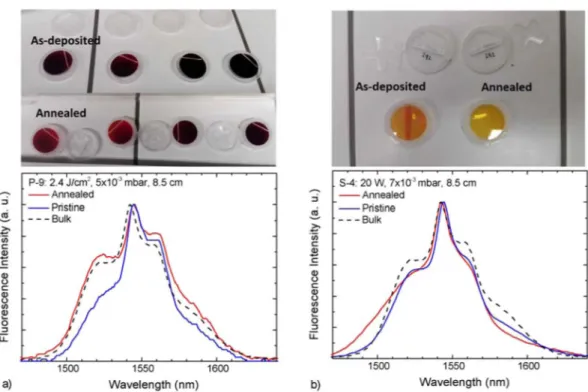
The effects of annealing on the fluorescence spectra can be observed directly in Fig. 7. One can notice that the changes in spectral band shape are more pronounced in the case of PLD samples. This phenomenon suggests that the fluctuations previously observed in as-deposited PLD films spectra are due to the inhomogeneity of the local lattice environment around the Er3+ ion positions, rather than an effect of fluorescence reabsorption,
as well as of the greater degree of film stress removal by annealing. Several samples (both PLD and sputtered) show a tendency to increase the intensity ratio for the short-wavelength emission contributions compared to the longer-wavelength ones: this could signify a reduction in the aforementioned self-absorption after the annealing, which is potentially associated to the band-gap energy variation with the annealing. However, since it is not a change that takes place consistently across the samples, one cannot ascribe the shape variation only to this phe-nomenon. From the comparison with the bulk emission band at 1.55 µm, it can also be noticed that PLD films have a more similar emission band shape to that of bulk glass, which in turn suggests a more similar local amor-phous structure in the vicinity of erbium centers, and are more clearly affected by reabsorption than sputtered films. On the contrary, the sputtered samples display a smoother, narrower emission band shape.
The 980 nm emission was also collected for various samples. The shape of the emission band is rather stable across samples, and the intensity seems to vary depending on the deposition parameters similarly to the 1.55 µm emission. The observation of emission peak around 1060 nm, which is not consistent with regular Er3+
fluores-cence, suggests the presence of neodymium contaminants in the glass substrate, which contributes to hinder the erbium emission and was observed in previous works.
Fluorescence spectra under 808 nm excitation were collected to include both the 4I
11/2→4I15/2 and 4I13/2→4I15/2
transitions in order to observe the variation of the intensity ratio between the two emission bands. The measure-ment was performed on a bulk sample (a fragmeasure-ment of the sputtering target, Fig. 8 - green line), and the samples with highest overall fluorescence intensity, one PLD (P-10, Fig. 8 - blue line) and one sputtered (S-12, Fig. 8
- red line). The first observation is that the 1550 versus 980 nm emission intensity ratio is quite different from that of previous works on similar materials (Moizan et al.35), where the ratio for Ga-Ge-Sb-S bulk glass with
1000 ppm Er3+ doping is in favor of the 980 nm peak, while in our measurements the latter is sensibly lower
than the 1550 nm one. This difference could be attributed to a more pronounced effect of energy transfer and
Figure 5. Raman scattering spectra of as-deposited Er3+-doped Ga-Ge-Sb-S thin films prepared by (a) PLD
(target-to-substrate distance 6 cm) and (b) RF magnetron sputtering (power 20 W, target-to-substrate distance 5 cm).
Figure 6. Photoluminescence spectra of Er3+-doped Ga-Ge-Sb-S thin films prepared by (a) PLD and (b) RF
magnetron sputtering, collected exciting at 980 nm.
Figure 7. Comparison of fluorescence spectra before and after annealing for (a) PLD films and (b) sputtered
cross-relaxation from the 4I
11/2 level in our samples, due to the higher Er3+ concentration. Moreover, it was
thought that a portion of the material in deposited thin films may be crystalline, which would further contribute to favor the energy transfer processes due to the -in average- higher host matrix crystal field. However, no clear suggestion of crystallite formation was visible from spectroscopy measurements, as no structuring of the emission peaks indicates the presence of crystalline phase, which is in agreement with observations in previous works24,
suggesting that the change in the aforementioned emission ratio is purely an effect of optical quenching due to the high dopant concentration. In addition, the measurements show that the intensity ratio shifts further in favor of the 4I
13/2→4I15/2 emission in deposited thin films, and in fact, the effect is more pronounced in PLD samples. This
phenomenon is attributed to the presence of structural defects in the material, especially in the proximity of active ion sites, which greatly increase the probability of non-radiative relaxation processes, and therefore correspond-ingly reduce the 4I
11/2 population. This is in agreement with the observation of PLD samples being in general
slightly rougher, presenting higher proportion of “wrong” bonds or defects than sputtered samples (suggesting a somewhat greater degree of structural inhomogeneity).
The luminescence in the MWIR range was assessed for bulk sputtered target, PLD and sputtered films by excit-ing at 808 nm and collectexcit-ing the emission around 2.7 µm, correspondexcit-ing to the 4I
11/2→4I13/2 emission. Although in
several films, it was possible to observe the expected emission band, the signal-to-noise ratio was very low due to the non-propagating geometry used for the standard spectroscopy measurements. The objective of this study was not to obtain a high-intensity MWIR emission that would require photolithography and waveguide etching, but simply to check whether thin layers with the highest intensity at 1.5 µm can actually emit around 2.7 µm.
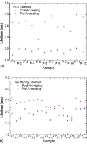
The lifetimes of 1.55 µm fluorescence were obtained fitting the time-resolved emission intensity data with single-exponential decay functions. The resulting lifetime values before and after annealing were compared. One can clearly assess (Fig. 9) that the annealing process causes an increase in fluorescence lifetime both for sputtered and PLD samples, but much more accentuated for the latter. In fact, the lifetimes of PLD samples, which were sen-sibly lower than those of the sputtered films before annealing, are now very similar to them. This fact could also support the claim that the annealing has a greater effect on PLD samples due to the larger number of structural defects within the latter, in as-deposited state.
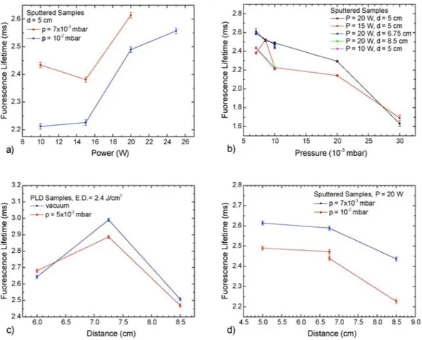
With these data at hand, one can examine the dependence of both fluorescence intensity and fluorescence lifetime on the deposition parameters. Figure 10 shows the behavior of fluorescence lifetimes as functions of dep-osition pressure, target-to-substrate distance, and RF power. While it is not possible to extrapolate a well-defined trend of fluorescence intensity as a function of laser energy density, RF power, target-to-substrate distance and argon pressure in the chamber, one can deduct from Fig. 10 some definite behaviors. In particular, while the lifetime of PLD samples cannot be clearly described as a function of either energy density or Ar pressure, one can identify the dependency of the sputtered samples lifetimes as a function of power and pressure: the sputtered films lifetimes tend to increase along with the power applied to the cathode, and decrease with increasing Ar pres-sure. Moreover, the lifetime of sputtered samples follows a decreasing trend as a function of target-to-substrate distance; however, the same does not apply to PLD samples (Fig. 10c), where it seems the lifetime has a maximum within the range considered, as it is highest for the samples deposited at 7.25 cm.
In general, we can also remark that PLD samples have a much less clear dependency on the deposition param-eters, as though their properties do vary with them, they do not have a univocal relationship to pressure and energy density. On the other hand, the sputtered samples plots suggest an increase in the fluorescence lifetime with increasing applied power during deposition (Fig. 10a), and a decrease with increasing Ar pressure (Fig. 10b), while a straightforward behavior of fluorescence intensity as a function of laser energy density, power, or Ar pressure is almost impossible to define. It is worthwhile to point out that the lifetimes and fluorescence intensities appear to follow opposite trends in the case of PLD as function of pressure and distance, which is consistent with the general expectation of lifetime and intensity being inversely proportional (compare Fig. 10c,d), while this relation is not as evident in the other cases. It is thought that the lack of this proportionality be due to the strong
Figure 8. Emission spectra under 808 nm excitation, showing the ratio between the 4I
11/2→4I15/2 and the 4I
presence of the non-radiative relaxation processes from the 4I
13/2 level, possibly rising from the presence of the
structural defects, as observed when exciting at 808 nm.
Methods
Chalcogenide glasses with the intent of obtaining a nominal composition of Ga5Ge20Sb10S65 and doped with Er3+
(0.5 wt.%) were prepared by means of conventional melt and quenching method. Glasses were synthesized from high purity (5 N) commercial elements17,24,35. Sulfur was further pre-purified by a static distillation. Elements
were weighted in a dry gloves box in appropriate amounts and introduced in a silica ampoule under vacuum for few hours. Then, the ampoule was sealed and elements were heated in a rocking furnace at 900 °C during 12 hours to ensure the homogenization of the melt. After the quenching in water, the glass was annealed below the glass transition temperature (Tg ≈ 305 °C) for 3 hours. Targets were obtained after slicing and polishing the glass rods.
Chalcogenide targets were prepared in the form of glass cylinders, 3 mm thick with a 25 and 50 mm diameter for PLD and RF magnetron sputtering deposition respectively17,24. The actual compositions were Ga
5Ge19Sb10S66 and
Ga4Ge19Sb9S68, for the PLD and sputtering targets respectively.
Er3+-doped Ga-Ge-Sb-S thin films were obtained by PLD (named from P-1 to P-12) and by RF magnetron
sputtering (named from S-1 to S-18) (Table 1)17,24. In the case of PLD deposition, chalcogenide targets were
ablated with a KrF excimer laser emitting at 248 nm using 160, 120 and 85 (±3) mJ output pulse energies, pulses duration of 30 ns and 20 Hz repetition rate. Laser energy densities were set at 2.4, 2.1 and 1.7 J/cm2 depending
on pulse energy. Various Ar pressures were used during deposition: 5·10−2 (Ar flow 75 sccm), 5·10−3 (Ar flow 25
sccm), 5·10−4 mbar (Ar flow 15 sccm) and no Ar gas (vacuum about 2·10−7 mbar). In order to obtain uniform film
thickness, the off-axis PLD technique combining rotating substrates and targets was used. Rotation speeds were about 15 and 30°/sec for targets and substrates respectively. Substrates were positioned parallel to the target sur-face at a distance of 6, 7.25, and 8.5 cm. In the case of RF magnetron sputtering, considering the insulator charac-ter of the chalcogenide target, sputcharac-tered films were deposited at low RF working power: from 10 to 25 W. In order to study the influence of Ar pressure, five Ar working pressures were applied for the sputtering process: 7·10−3,
8.5·10−3, 1·10−2, 2·10−2 and 3·10−2 mbar (Ar flow was set at 75 sccm for all sputtering depositions). An off-axis
substrate rotation (30°/sec) was used during deposition while substrates were positioned at a target-to-substrate distance of 5, 6.75 and 8.5 cm. Substrates were silicon wafer (10 mm × 15 mm) and glass (1″) and time deposition was chosen to obtain similar thickness of about 4 and 3 µm for PLD and sputtered films, respectively.
Figure 9. 1.55 µm fluorescence lifetimes of PLD and sputtered films before and after the annealing for (a) PLD films and (b) sputtered films.
The chemical composition of Er3+-doped Ga-Ge-Sb-S targets and films were studied by scanning electron
microscopy with an energy-dispersive X-ray analyzer (SEM-EDS, JSM 6400-OXFORD Link INCA) collecting the spectra over a roughly 0.01 mm2 area for each sample. Atomic percentage of each element (±0.5% and ±1% for
the targets and the films, respectively) was extracted exploiting LLLK lines of Ga, Ge, Sb and S element working at 10 kV.
The morphology and the topography of pulsed laser deposited and sputtered films were analyzed by atomic force microscopy (AFM, Ntegra Prima, NT-MDT). The tapping mode imaging was used on area of 2 µm × 2 µm and 5 µm × 5 µm. The SEM technique was also applied to observe thin films morphology using a field emission gun SEM (JSM 6301 F).
Linear refractive indices of pulsed laser deposited, sputtered films and chalcogenide targets were obtained from the analysis VASE data measured using a rotating analyzer ellipsometer measuring in UV-Vis-NWIR (300– 2500 nm) (J.A. Woollam Co., Inc., Lincoln, NE, USA). The VASE data were recorded at three angles of incidence (65°, 70° and 75° for thin films and 50°, 60° and 70° for targets). The resolution was set to 5 nm for the films considering the estimated thickness of chalcogenide films and 20 nm for Er3+-doped Ga-Ge-Sb-S targets. The
Cody-Lorentz model36,37 was used to analyze VASE data. This model is appropriate for the description of
amor-phous chalcogenide optical functions38. The thickness of chalcogenide thin films was also determined by VASE
data analysis.
The recorded Raman scattering spectra for Er3+-doped Ga-Ge-Sb-S bulk targets and films deposited by pulsed
laser or sputtered by RF magnetron were collected by a LabRam HR800 spectrometer (Horiba Jobin-Yvon) equipped with a laser emitting at 785 nm (Toptica), an Olympus BX41 microscope with 100X objective and a confocal aperture. Raman spectroscopy is known to be a non-destructive technique: the laser power has been adjusted on the samples so that they are not damaged or modified under the excitation laser beam.
The optical and spectroscopic properties of the Er3+-doped films were obtained via fluorescence spectroscopy
and lifetime measurements. An 808 and a 980 nm laser diode were used to excite the films and obtaining the emission of erbium at 1.55 µm by focusing the beam onto the sample. The luminescence was collected via a mon-ochromator leading to an InGaAs detector. The same setup was used for investigating the NWIR emission bands at 980 nm and 1.55 µm and the MWIR emission band at ~2.7 µm, using a nitrogen-cooled InSb detector and exciting at 808 nm. The excitation beam was modulated at a 20 Hz frequency, and the emission intensity signal was processed through a lock-in amplifier to reduce environmental noise in the collection of fluorescence spectra.
Lifetime measurements were performed with a similar setup, using an oscilloscope, and using the modulation frequency signal from the diode drive as the trigger. The collected signal was averaged over more than 500 cycles to improve the signal-to-noise ratio.
Figure 10. Plot of fluorescence lifetimes versus the different deposition parameters for sputtered samples
The thin films samples were annealed below the glass transition temperature of corresponding glass target. The annealing was performed in a horizontal furnace: heating proceeded from room temperature up to 290 °C over a period of 4 hours and 30 minutes, then lingering at 290 °C for 2 hours, and cooling down naturally to room temperature overnight. The fluorescence and lifetimes of the annealed samples were then collected and compared to those obtained before the treatment.
Conclusions
The development and characterization of optically active thin films from erbium-doped Ga-Ge-Sb-S glass opens the way for several applications in the infrared range. In this work, the results of two PVD methods, namely RF sputtering and PLD, for the fabrication of micrometer-thick films were compared. This study provides an exten-sive description of the effects of the different deposition parameters on the composition of the end product and on its optical and spectroscopic properties. It can be concluded that the most prominent factor for the optical properties of the films is the sulfur content, which will change the band-gap energy and the refractive index of the thin sulfide films doped with erbium ions. In turn, one can see that the latter is particularly affected by chamber pressure during deposition. The understanding of how the deposition parameters affect the composition, and therefore the properties of the resulting films, allows the fabrication of planar waveguides designed according to the specific needs of their intended application, such as sensing, signal manipulation, or the amplification of light. PLD and sputtering approaches have distinct advantages and disadvantages. PLD films have a more con-sistent composition-wise with respect to a possible variation in deposition parameters and their deposition rate is higher, making them a rather reliable deposition method. However, they strongly require an annealing process to homogenize the structure of the active ion centers and their optical properties appear more erratic, not show-ing well-define trends as a function of the deposition parameters and therefore less predictable. The properties of the sputtered films depend more strongly on the deposition parameters, making this method interesting for the fabrication of multi-layer or graded-index structures with a single target, and for tailoring the composition by controlling the deposition conditions. This deposition technique shows here its good suitability as rare earth doped chalcogenide films are necessary for applications without the need for post-deposition treatments.
Data availability
The datasets generated and analyzed during the current study are available from the corresponding author on reasonable request.
Received: 7 February 2020; Accepted: 9 April 2020; Published: xx xx xxxx
References
1. Singh, V. et al. Mid-infrared materials and devices on a Si platform for optical sensing. Sci. Technol. Adv. Mater. 15, 014603 (2014). 2. Lee, B. G. et al. Widely tunable single-mode quantum cascade laser source for mid-infrared spectroscopy. Appl. Phys. Lett. 91,
231101 (2007).
3. Dettenrieder, C., Raichlin, Y., Katzir, A. & Mizaikoff, B. Toward the Required Detection Limits for Volatile Organic Constituents in Marine Environments with Infrared Evanescent Field Chemical Sensors. Sensors 19(17), 3644 (2019).
4. Shaw, L. B., Cole, B., Thielen, P. A., Sanghera, J. S. & Aggarwal, I. D. Mid-wave IR and long-wave IR laser potential of rare-earth doped chalcogenide glass fiber. IEEE J. Quantum Electron. 37(9), 1127–1137 (2001).
5. Schweizer, T., Samson, B. N., Moore, R. C., Hewak, D. W. & Payne, D. N. Rare-earth doped chalcogenide glass fibre laser. Electron.
Lett. 33(5), 414–416 (1997).
6. Park, B. J. et al. Dy3+ doped Ge–Ga–Sb–Se glasses and optical fibers for the mid-IR gain media. J. Ceram. Soc. Jpn 116(1358),
1087–1091 (2008).
7. Eggleton, B. J., Luther-Davies, B. & Richardson, K. Chalcogenide photonics. Nature Photonics 5, 141–148 (2011).
8. Pelusi, M. D. et al. Applications of Highly-Nonlinear Chalcogenide Glass Devices Tailored for High-Speed All-Optical. Signal
Processing. IEEE J. Sel. Top. Quant 14, 529–539 (2008).
9. Guignard, M. et al. Chalcogenide Glasses Based on Germanium Disulfide for Second Harmonic Generation. Adv. Funct. Mater. 17, 3284–3294 (2007).
10. Verger, F. et al. RF sputtered amorphous chalcogenide thin films for surface enhanced infrared absorption spectroscopy. Opt. Mater.
Express 3(12), 2112–2131 (2013).
11. Baudet, E. et al. Development of an evanescent optical integrated sensor in the mid-infrared for detection of pollution in groundwater or seawater. Adv. Device Mater 3(2), 23–29 (2017).
12. Baudet, E. et al. Experimental design approach for deposition optimization of RF sputtered chalcogenide thin films devoted to environmental optical sensors. Sci. Rep 7, 3500 (2017).
13. Bouška, M. et al. Pulsed laser deposited GeTe-rich GeTe-Sb2Te3 thin films. Sci. Rep 6, 26552 (2016).
14. Seddon, A. B. Mid-infrared (IR) – A hot topic: The potential for using mid-IR light for non-invasive early detection of skin cancer in vivo. Phys. Status Solidi B 250(5), 1020–1027 (2013).
15. Jin, T., Zhou, J., Lin, H.-Y. G. & Lin, P. T. Mid-Infrared Chalcogenide Waveguides for Real-Time and Nondestructive Volatile Organic Compound Detection. Anal. Chem. 91(1), 817–822 (2019).
16. Han, Z. et al. On-chip chalcogenide glass waveguide-integrated mid-infrared PbTe detectors. Appl. Phys. Lett. 109(7), 071111 (2016).
17. Nazabal, V. et al. Luminescence at 2.8 μm: Er3+-doped chalcogenide micro-waveguide. Opt. Mater. 58, 390–397 (2016).
18. Ramachandran, S. & Bishop, S. G. Excitation of Er3+ emission by host glass absorption in sputtered films of Er-doped Ge
10As40Se25S25
glass. Appl. Phys. Lett. 73, 3196 (1998).
19. Frantz, J. A., Shaw, L. B., Sanghera, J. S. & Aggarwal, I. D. Waveguide amplifiers in sputtered films of Er3+- doped gallium lanthanum
sulfide glass. Opt. Express 14, 1797–1803 (2006).
20. Vigreux-Bercovici, C., Pradel, A., Fuchs, A. & Fick, J. Effect of annealing on the photoluminescence in sputtered films of Er-doped chalcogenide glasses. Phys. Chem. Glasses 47, 162–166 (2006).
21. Imai, T., Maeda, K., Fujita, M. & Saito, N. Photoluminescence properties of erbium-doped amorphous gallium-germanium-selenium films fabricated by RF sputtering. Phys. Status Solidi C 6(1), S106–S109 (2009).
22. Borisov, E. N., Smirnov, V. B., Tverjanovich, A. & Tveryanovich, Y. S. Deposition of Er3+ doped chalcogenide glass films by excimer
23. Dwivedi, P. K. et al. Rare-earth doped chalcogenide thin films fabricated by pulsed laser deposition. Appl. Surf. Sci. 248(1-4), 376–380 (2005).
24. Nazabal, V. et al. Optical waveguide based on amorphous Er3+-doped GeGaSbS(Se) pulsed laser deposited thin films. Thin Solid
Films 518, 4941–4947 (2010).
25. Albarkaty, K. S. et al. Erbium-doped chalcogenide glass thin film on silicon using femtosecond pulsed laser with different deposition temperatures. Appl. Phys. A 125, 1 (2019).
26. Ivanova, Z. G., Koughia, K., Tonchev, D., Pivin, J. C. & Kasap, S. O. Photoluminescence in Er-implanted amorphous Ge-S-Ga thin films. Journal of Optoelectronics and Advanced Materials 7, 1271–1276 (2005).
27. Lyubin, V., Klebanov, M., Sfez, B. & Ashkinadze, B. Photoluminescence and photodarkening effect in erbium-doped chalcogenide glassy films. Mater. Lett. 58, 1706–1708 (2004).
28. Yan, K., Vu, K. & Madden, S. Internal gain in Er-doped As2S3 chalcogenide planar waveguides. Opt. Lett. 40, 796–799 (2015). 29. Bodiou, L. et al. Mid-infrared guided photoluminescence from integrated Pr3+-doped selenide ridge waveguides. Opt. Mater 75,
109–115 (2018).
30. Ari, J. et al. Co-doped Dy3+ and Pr3+ Ga
5Ge20Sb10S65 fibers for mid-infrared broad emission. Opt. Lett. 43(12), 2893–2896 (2018).
31. Abdellaoui, N. et al. Tb3+ doped Ga
5Ge20Sb10Se65-xTex (x = 0-37.5) chalcogenide glasses and fibers for MWIR and LWIR emissions.
Opt. Mater. Express 8(9), 2887–2900 (2018).
32. Starecki, F. et al. Dy3+ doped GaGeSbSe fiber long-wave infrared emission. J. Lumin. 218, 116853 (2020).
33. Adam, J.-L., & Zhang, X. H. Chalcogenide Glasses: Preparation, properties and application (Woodhead Publishing series in Electronic and Optical Materials) p. 281 (2014).
34. Baudet, E. et al. Structural analysis of RF sputtered Ge-Sb-Se thin films by Raman and X-ray photoelectron spectroscopies. J.
Non-Cryst. Solids 444, 64–72 (2016).
35. Moizan, V. et al. Er3+-doped GeGaSbS glasses for mid-IR fibre laser application: Synthesis and rare earth spectroscopy. Opt. Mater.
31, 39–46 (2008).
36. Jellison, G. E. & Modine, F. A. Parameterization of the optical functions of amorphous materials in the interband region. Appl. Phys.
Lett. 69, 2137–2137 (1996).
37. Ferlauto, A. S. et al. Analytical model for the optical functions of amorphous semiconductors from the near-infrared to ultraviolet: Applications in thin film photovoltaics. J. Appl. Phys. 92, 2424–2436 (2002).
38. Halenkovič, T. et al. Linear and nonlinear optical properties of co-sputtered Ge-Sb-Se amorphous thin films. Opt. Lett. 45(6), 1523–1526 (2020).
Acknowledgements
The authors would like to thank to the project of International Mobility of Researchers at the University of Pardubice, OP RDE project CZ.02.2.69/0.0/0.0/16_027/0008008 as well as to Czech Science Foundation (Project No. 19-24516 S), COST MP1401-STSM, CNRS, Brittany Region.
Author contributions
V.N. planned and managed the project; E.B. and J.G. performed the sample fabrication; E.B., G.L. and S.N. performed the experiments and analyzed the data with the help of V.N., P.N., M.B., Y.L. and Y.M.; S.N. and G.L. performed the spectroscopic measurements at ISCR in Rennes and CIMAP in Caen, France with the help of F.S. and J.L.D.; E.B. and S.N. wrote the manuscript with the help of G.L., J.L.A., V.N., and P.N. concerning the comparison of chalcogenide thin films deposited by different PVD approaches.
competing interests
The authors declare no competing interests.
Additional information
Correspondence and requests for materials should be addressed to V.N. Reprints and permissions information is available at www.nature.com/reprints.
Publisher’s note Springer Nature remains neutral with regard to jurisdictional claims in published maps and
institutional affiliations.
Open Access This article is licensed under a Creative Commons Attribution 4.0 International
License, which permits use, sharing, adaptation, distribution and reproduction in any medium or format, as long as you give appropriate credit to the original author(s) and the source, provide a link to the Cre-ative Commons license, and indicate if changes were made. The images or other third party material in this article are included in the article’s Creative Commons license, unless indicated otherwise in a credit line to the material. If material is not included in the article’s Creative Commons license and your intended use is not per-mitted by statutory regulation or exceeds the perper-mitted use, you will need to obtain permission directly from the copyright holder. To view a copy of this license, visit http://creativecommons.org/licenses/by/4.0/.