HAL Id: hal-02868237
https://hal.archives-ouvertes.fr/hal-02868237
Submitted on 15 Jun 2020
HAL is a multi-disciplinary open access
archive for the deposit and dissemination of
sci-entific research documents, whether they are
pub-lished or not. The documents may come from
teaching and research institutions in France or
abroad, or from public or private research centers.
L’archive ouverte pluridisciplinaire HAL, est
destinée au dépôt et à la diffusion de documents
scientifiques de niveau recherche, publiés ou non,
émanant des établissements d’enseignement et de
recherche français ou étrangers, des laboratoires
publics ou privés.
Deep reactive ion etching process for PZT actuators
Djaffar Belharet, Vincent Chalvet, Cédric Clevy, Micky Rakotondrabe,
Laurent Robert
To cite this version:
Djaffar Belharet, Vincent Chalvet, Cédric Clevy, Micky Rakotondrabe, Laurent Robert. Deep
reac-tive ion etching process for PZT actuators. Journees Nationales sur les Technologies Emergentes en
Micronanofabrication, Nov 2015, Lyon, France. �hal-02868237�
Deep reactive ion etching process for PZT actuators
D.Belharet
1, V.Chalvet
2, C.Clevy
2, M. Rakotondrabe
2, L. Robert
11
MIMENTO, FEMTO-ST, UMR 6174, Besançon, France
2
AS2M Department, FEMTO-ST, UMR 6174, Besançon, France
E-mail address: [email protected]
Topic : Etching and Surface Processing
Abstract— We developed a deep etching
plasma process on PZT substrate that has
been optimized to obtain a good anisotropy
and smooth side walls. Cantilevered piezo
actuators have been fabricated and tested in
order to verify that the process does not
modify
the
PZT
properties.
The
characterization show that the bandwidth of
the 4mm-long actuators exceeds 1772Hz and
the static deflection coefficient reaches
1.25µm/V, which matches well the theory.
These results demonstrate the efficiency of the
process to maintain the materials properties.
I. INTRODUCTION
Lead Zirconate Titanate (PZT) thin films are known for their applications in micro electro-mechanical system (MEMS) because of their superior piezoelectric and pyroelectric properties and in memory devices, such as nonvolatile ferroelectric random access memories (FRAM), because of their high dielectric constants and bistable polarization [1]. To incorporate/integrate these materials into silicon IC technology it is necessary to develop anisotropic dry etch processes to etch desired, precisely accurate and defect free PZT structures in the micrometer size range.
The PZT ferroelectric thin films that compose piezoelectric elements react poorly with halogen gases and their halides have low vapor pressures. For these reasons, these materials are called hard-to-etch materials. One of the widely used dry etching processes is halogen plasmas - chlorine and fluorine based gases which have shown high potential to achieve the desired results [2,3,4].
In this paper, we propose process optimization using Ar/C4F8 in order to etch anisotropically the PZT structures and also to obtain an acceptable etch rate. The other objective is to obtain a good smoothing in the walls trenches. PZT actuators with cantilever structure (length of 4mm, total thickness of 53µ m, width varying from 150µ m to 1mm) have been afterwards realized with the new process. In order to check if this process does not modify the properties of the PZT materials, we characterized the
fabricated actuators. The results show that the bandwdith, which in excess of 1772Hz, as well as the static property, reaching 1.25µm/V, almost correspond to the theory demonstrating that the mechanical and the electromechanical properties were not influenced by the process.
II. PROCESS FLOW
A. Stack wafer preparation
The fabrication process starts from a 4” Si substrate. A PZT substrate is bond on it by using an Au/Au wafer bonding process and then thinned to 48 µm. A thin photoresist film is deposited on the PZT wafer, than it’s bonded with silicon wafer in order to be polished. A thin layer Cr/Au is deposited on the PZT polished wafer backside. While doing this operation, a thin layer Cr/Au is deposited The (SOI) silicon on insulator wafer frontside. The stack wafer followed several process steps. The critical process operation is the PZT etching. This operation needs hard mask which is achieved by the electroplating process.
B. Electroplating process
The electroplating of the Nickel mask was achieved by using the Technotrans Microform 100 industrial tool. A Ni layer was electroplated on an Au seed layer, which guarantees the electrical conduction required for the process, using a direct current. The concentration of the electroplating solution is: [Ni]=89g/l. Boric acid ([H3BO3]=55g/l) allows to buffer the solution to pH = 3,6 and the temperature of the electrolyte is fixed at 52°. This machine and these process conditions ensure reproducible deposition rate estimated at 15,2 µ m/h. The Ni electroplated thickness is 9,7 µ m.
C. DRIE Process
The DRIE etching process was achieved on STS PEGASUS equipment. The ICP coil power was fixed at 600W, the bias power was varied and optimized at 300W, the chamber pressure was 2mTorr. The temperature was set to 0° and the gas ratio Ar/C4F8 was kept at 64 sccm /5 sccm.
The geometry of the PZT cantilevers was then characterized by using profilometer and SEM microscopy. The figure 1 shows the SEM cross section of PZT structures and the sidewall profile angle obtained after the DRIE process.
.
(a) (b)
Figure 1. (a) SEM cross section of etched PZT structures (b) side wall etched angle
The characterization results showed that the etch rate is 800A°/min, the profile angle is 82° as illustrated in the figure 1 and the selectivity is 1:15. The DRIE process was optimized to obtain smoother sidewalls. We studied the effect of critical process parameters and one of them is the substrate power (Bias). The substrate power determines the kinetic energy of the ions bombarding the substrate. As the substrate power increases, the ions are accelerated making up a high energy bombardment of the wafer. This high energetic sputtering by ions causes an increase in the etch rate by facilitating rapid physical removal of non-volatile etch products from the surface of the sample [5,6]
III. FABRICATED PZT CANTILEVERS ACTUATORS
The new process was afterwards used to fabricate piezoelectric cantilever actuators. The sizes of the cantilevers are: 4mm x 53µm (length x total thickness), where the thickness of the PZT is 48µm and the thickness of the passive material (silicon) is 5µm. The width varies from 150µm to 1mm. Fig.2 presents the different cantilevered actuators as well as the experimental setup. The setup is composed of: the actuators to be characterized, an optical sensor (resolution 10nm, bandwidth in excess of 5 kHz) from Keyence-company, a computer and the Matlab-Simulink software to manage the signals (voltage and measurement), a dSPACE acquisition board that serves as interface, and a voltage amplifier (+-200V).
Figure 2. The fabricated actuators IV. CARACTERISATION RESULTS
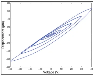
Both the static and the dynamic properties of the actuators were characterized. The static property is
obtained by applying a sine voltage to the actuators. The frequency is chosen to be low: 0.1Hz. The output displacement is afterwards plotted versus the input voltage. Fig. 3 show the results when the voltage amplitude is 5V, 10V, 20V, 30V, 40V, which show a gain of 1.25µm/V. A harmonic analysis was also carried out to the actuators and it was shown that the bandwidth reaches 1772Hz. These results are in good agreement with the theory and demonstrate that the process does not modify the mechanical as well as the electromechanical properties of the materials. Therefore, they show that it is possible to machine even more miniaturized PZT based actuators without compromising the materials characteristics. Furthermore, such miniaturized actuators are more performant in term of gain and frequency relative to classically sized PZT cantilevers; see for instance [7].
Figure 3. Static property I. CONCLUSION
The etching process for PZT thin films was developed to obtain the high etch rate (800A°/min) and reasonable selectivity 1:15 without redeposits and residues. The sidewall angle of etched PZT films was 82°. The characterization showed that the bandwidth of the actuators exceeds 1772Hz and the static property reaches 1.25µm/V.
ACKNOWLEDGMENT
This work has been supported by the french RENATECH network and its FEMTO-ST technological facility.
REFERENCES
[1] C. W. Chung, J. Vac. Sci. Tech. B 16, 1894 (1998).
[2] D.P.Vijay and S.B.Desu, J. Electrochem. Soc., 140(9), pp2640-2645,1993.
[3] H. Archard,, H. Mace, L.;Peccoud, Microelectron. Eng, Vol.29, pp19-28, 1995
[4] M. Bale and R. E. Palmer, Deep plasma etching of piezoelectric PZT with SF6, J. Vac. Sci. Technol. B 19, 2020 2001
[5] S.S. Subasinghe, A.Goyal and S.A. Tadigadapa, Proc. of SPIE Vol. 6109, 61090D, 2006
[6] D.L. Flamm, V. M. Donnelly and D.E. Ibbotson, , J. Vac. Sci. Technol. B 1, 23? 1983
[7] M.Rakotondrabe, Y. Haddab and P.Lutz, IEEE - Transactions on Control Systems Technology (T-CST), Vol.17, Issue 3, pp:528-539, May 2009.