1
AlN films deposited by dc magnetron sputtering and high power impulse
magnetron sputtering for SAW applications.
K. Ait Aissa1, 2*, A. Achour3, O. Elmazria2, Q. Simon1, M. Elhosni2, P. Boulet2, S. Robert2 and M. A. Djouadi1.
1Institut des Matériaux Jean Rouxel, Université de Nantes, UMR 6502 CNRS, 2 rue de la
Houssinière B.P. 32229 - 44322 Nantes cedex 3, France.
2Institut Jean Lamour (IJL), Université de Lorraine, UMR 7198 CNRS, Boulevard des
Aiguillette, 54506 Vandoeuvre Lès Nancy, France.
3LAAS (CNRS), 7 Avenue du Colonel Roche, 31400 Toulouse, France
*To whom correspondence should be addressed
E-mail: keltouma.ait-aissa@insa-rouen.fr
Abstract
In this work, AlN films were deposited on silicon substrates buffered by epitaxial AlN thin film for surface acoustic wave (SAW) applications. The films were deposited by dc magnetron sputtering (dcMS) and high power impulse magnetron sputtering (HiPIMS) deposition techniques. The structural properties of AlN films were investigated using X-ray diffraction (XRD), Raman spectroscopy and atomic force microscopy. In both cases of films deposited by dcMS and HiPIMS, the XRD results showed that the obtained films are oriented, with a full width at half maximum rocking curves of around 1°. Raman spectroscopy revealed higher residual stress relaxation in the AlN epilayers grown by HiPIMS compared to AlN grown by dcMS, highlighted by a blue shift in the E2(high) Raman mode. The SAW measurements indicated an insertion loss of AlN/Si -SAW devices of about 53 and 35 dB for the AlN films deposited by dcMS and HiPIMS respectively. The relation between the
2 structural properties of AlN and the characteristics of AlN-SAW devices were correlated and discussed.
Keywords: Aluminum nitride, Physical vapor deposition, HiPIMS, Surface acoustic wave.
1. Introduction
Surface acoustic wave (SAW) devices are receiving an increasing interest in recent years due to their wide spread applications as resonators, filters, sensors and actuators. In order to achieve high performance of such SAW devices, it is desirable to integrate a material which insures high frequency ranges, large electromechanically coupling factor (Ks2), and
temperature stability of the corresponding device. Materials in the form of thin films such as zinc oxide (ZnO) [1] and aluminum nitride (AlN) [2,3] have been proposed for those applications. The quality of these integrated films, their characteristics and growth supports, also, monitor the performance of the SAW devices. AlN film with c-axis preferred orientation is attractive for SAW applications, because of its high surface acoustic wave (SAW) velocity [4], appreciable (Ks2), and high-temperature stability. In view of its different applications,
AlN films have been deposited on various substrates such as lithium niobate [5], sapphire [2,6], diamond [7] and silicon (Si) [8]. It is noteworthy to mention, that the Si substrate is promising for group III metal nitride integration with the cheap and well-developed technology. Therefore, AlN deposition on Si substrate for SAW devices, will add flexibility to the design of technology for practical application, due to simple process, simple device structure and low cost. To deposit AlN films, various techniques such as metal-organic vapour deposition [9], chemical vapour deposition [10] and molecular beam epitaxy [11] were used. Nonetheless, most of these techniques require high substrate temperatures (in the range of 600-1200 °C) which are not compatible with C-MOS technology. Moreover, these techniques
3
produce, usually, AlN films with high surface roughness, which is detrimental to wave propagation especially when high frequency is reached [12]. Reactive magnetron sputtering techniques such as dc-magnetron sputtering (dcMS) and High power impulse magnetron sputtering (HiPIMS) can produce high quality AlN films at lower deposition temperature with guaranteed uniformity of film thickness and low surface roughness [13], along with a full compatibility with C-MOS process [14].In this work, AlN films were deposited by dcMS and HiPIMS configurations on Si substrates buffered by epitaxial AlN thin film. The structural quality and morphology of the films were assessed by X-ray diffraction, Raman spectroscopy and atomic force microscopy. In the last part of this study, SAW devices based AlN/Si layered structures were realized using both deposition techniques dcMS and HiPIMS. SAW devices characterization will lead, on the one hand, to prove the piezoelectric quality of the deposited films and to compare their performances on regard of used deposition technique.
2. Experimental details
In this study, commercial templates of 200 nm thick AlN epitaxially grown on (111) Si substrates (KYMA Technologies) were used for the deposition of AlN films either by dc-magnetron sputtering (dcMS) or by High power impulse dc-magnetron sputtering (HiPIMS). For the deposition, a 99.9999% pure aluminum 2 inch target was used. The distance between the target and substrate holder was 30 mm. The system was pumped to a base pressure of 6×10⁻³
Pa with a turbo-molecular pump before introducing argon and nitrogen gases. The sputtering system employed an unbalanced magnetron cathode powered by a 150 W dc power supply in the case of dcMS configuration. In HiPIMS configuration, high voltage pulses are applied to the cathode by a custom-made power supply [15]. The applied voltage was -1 kV, with a pulse width of 28 µs, and frequency of 300 Hz.The experimental details are fully described in our previous works [16].
4
Before deposition, the target was cleaned using argon gas discharge plasma for 15 min followed by a pre-sputtering step, using the same conditions as the subsequent film deposition with a shutter shielding the sample. The total gas flux rate during deposition by the two processes (dcMS and HiPIMS) was maintained constant at 40 sccm while that of the reactive N2 gas was fixed at 35%. The sputtering pressure was fixed at 0.40 Pa in both dcMS and
HiPIMS. The substrates were in floating potential and were either additionally heated or cooled during the deposition. For a proper comparison of stress and crystallographic properties of different films, the deposition time was adjusted to maintain AlN film thickness constant. Time depositions was around 12 and 30 minutes for films deposited by dcMS and HiPIMS, respectively, which leads to film thicknesses of 500 nm in both configurations. The schematic structures of the samples are shown in Figure 1. The AlN buffer layer, AlN film deposited by dcMS and AlN deposited by HiPIMS are designed as samples (a), (b) and (c) respectively. Typical deposition parameters are shown in Table 1.
The thicknesses of the films were estimated by using a DEKTAK VEECO 8 profilometer. The crystal structure and crystallinity were investigated by X-ray diffraction in q-2q Bragg Brentano configuration (Siemens D5000 Moxtek diffractometer using Cu Kα radiation λ =
0.154184 nm) and in w-scan rocking curve and j-scan configurations (Bruker D8 Discover diffractometer using Co Ka radiation, l = 0.179026 nm). Raman scattering spectroscopy was carried out at room temperature by HORIBA Jobin Yvon HR800UV spectrometer in backscattering configuration, with z orthogonal to the substrate surface, and using the 325 nm lines of the (Cd-He) laser as the excitation source. The microstructural and surface morphology characterizations of the samples were examined by field emission gun scanning electron microscopy (SEM) (Carl-Zeiss) and atomic force microscopy (AFM) in contact mode (NanoWizard II BioAFM), respectively. To evaluate the piezoelectric and acoustic properties of deposited AlN films, SAW devices were realized in delay line
z d unpolarise x
5
configuration. The devices consisted of two identical inter-digitated transducers (IDT), with 50 pairs of fingers and a spatial periodicity of 24 μm, thus fixing the wavelength of acoustic wave at λ = 24 μm. The free space delay was fixed to 50 λ. The IDT are consisting of 100 nm thick aluminum (Al) film structured by conventional photolithography and wet etching. To eliminate the effects of both geometry and other parameters as finger's width/spacing ratio, Al film thickness uniformity on SAW resonator frequency, 100 nm Al film was deposited at the same time, and the same mask was employed for the structures during the SAW fabrication process. Frequency responses of SAW devices in transmission configuration (S21) were measured using Network Analyzer (Agilent PNA 5230A, Santa Clara, CA) and RF prober station RF (PM5Suss Micro-tech PM5).
3. Results and discussion
3.1. Structural and morphological characterization
The structural features of AlN films analysed in q-2q mode are presented in Figure 2(a) for the three investigated samples. The sole presence of peaks related to (002) plans of the wurtzite-type structure indicates that the AlN films were strongly c-oriented. As shown in Figure 2(a), the peak position of the sample (b) does not exhibit any shift compared to those of the epitaxial AlN buffer layer (i.e., sample (a)), suggesting that the sample (b) maintains the same type of tensile stress as the epitaxial AlN buffer layer [17], even when the film thickness of sample (b) is two times thicker than that of the epitaxial AlN buffer layer [18],on the contrary, sample (c), shows a broadened (002) peak from the epilayer that is shifted toward lower angles. In this case, two contributions may cause this shift: the first one comes from the epitaxial AlN buffer layer with a tensile residual stress and the second one originates from the AlN layer deposited by HiPIMS with a compressive residual stress. Indeed, the origin of the compressive residual stress in the case of the film deposited by HiPIMS (sample
6
(c)) can be attributed to the higher ionization rate as it has been reported in our previous works [17].
XRD rocking curve was carried out to investigate the crystalline quality of the epilayers as shown in Figure 2(b). The full width of half maximum (FWHM) of the (002) AlN rocking curve was approximately 1° (q) for both samples (b) and (c) which is the same of that of sample (a). This result suggests that AlN films grown on the epitaxial AlN buffer layer were oriented along the c-axis perpendicular to the substrate, indicating an excellent relationship and remarkable high crystalline quality of the deposited films. Furthermore, a variety of XRD phi-scans of the sample (c) is performed to establish the in-plane orientation alignment of the AlN films with respect to their corresponding underlying layers. Figure 2(c) shows phi-scans of (220) Si, (101) epitaxial AlN buffer layer and (101) AlN film reflections. The scan reveals that AlN thin film is a single crystal with AlN (002)/epitaxial AlN buffer layer/Si(111). The alignment between the AlN (101) peaks from the layer and the epitaxial AlN peak from the buffer layer indicates an epitaxial growth. The same results were obtained in the case of the film deposited by dcMS (not shown here).
Figure 3 shows the Raman spectra collected at room temperature from sample (a), (b) and (c). The peaks that are located at about 604 cm-1 and 649 cm-1 are attributed to the
A1(TO) and E2(high) Raman mode of AlN, respectively [19] (TO corresponds to transversal optical phonons). After AlN deposition (for sample b and c), the A1(TO) peak is found to weaken while the E2(high) peak became broader. The broadening of the E2(high) peak could be attributed to the crystalline deterioration or to the intrinsic stress [20]. Nevertheless, since the XRD analyses (Figure 2(b and c)) confirm the high crystalline quality of the deposited films, the hypothesis of crystalline deterioration can be excluded. The hypotheses of intrinsic stress are more accurate and supported by the blue shift of the E2(high) peak in case of sample (c) which at the same time exhibits larger broadening of this peak.
7
It should be noted that the E2(high) mode of the AlN buffer layer exhibits a red shift with respect to the standard value [19]. This shift of the E2(high) mode provides evidence for the tensile residual stress of the buffer layer [21]. After AlN deposition by dcMS process (i.e., sample (b)) the position of the E2(high) mode remains the same but with the presence of a shoulder at around 657 cm-1, which indicates a small change in the residual stress of this film.
On the other hand, after AlN deposition by HiPIMS, two peaks were clearly distinguishable. The first one at a position 649 cm-1 with a red shift with respect to the standard value [19]
corresponds to the E2(high) mode of epitaxial AlN buffer layer. The second one at 662 cm-1
with a blue shift with respect to the standard value corresponds to the E2(high) mode of AlN deposited by HiPIMS [19]. In fact, the E2(high) mode has been demonstrated previously to depend on biaxial strain [20,22]. In the case of the films deposited by HiPIMS (sample (c)), we have a kind of equilibrium of the biaxial strain, thanks to the presence of AlN buffer which introduces a compressive strain that counter balance the compressive strain of the film deposited by HiPIMS, which is in good agreement with XRD results.
The cross-sectional SEM images of the AlN films deposited on the epitaxial AlN buffer layer are shown in Figure 4. In both cases (Figure 4(a and b)), the AlN thin film exhibits numerous columnar grains which are perpendicular to the surface of substrate, and for quite similar thicknesses, the synthesized AlN does not show any significant variation in film morphology. The surface morphologies of samples (a), (b) and (c) were characterized by atomic force microscopy (AFM) as shown in Figure 5. The surface roughness in terms of root mean square (rms) were measured to be approximately 0.7, 2 and 1 nm for samples (a), (b) and (c), respectively, over a measured area of 2 μm by 2 μm. The granular surface can be clearly seen from the micrograph, ensuring a sufficiently smooth surface for SAW propagation. Indeed, when AlN film is used as active layer for SAW devices, its surface roughness has a critical impact on the performances of the device and mainly on the acoustic propagation losses.
8 Indeed This is because as the surface acoustic wave propagation is confined on the surface, the most acoustic energy is concentrated within a wavelength from the surface to the bulk.
3.2. SAW characterization
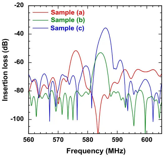
The SAW devices fabricated using the different structures were characterized, and IDT was realized on the top of the deposited AlN film. The frequency responses of the delay line in transmission configuration (S21) of the third mode (Rayleigh mode) are shown in
Figure 6. The surface acoustic wave velocity (V) of the structure AlN/Si was determined using the formula:
where f0 and λn are respectively the center frequency and the wavelength of the considered
peak. When a harmonic peak of order n is considered, then λn = P/n. P being the spatial period
(P = 24 µm in our case). The values of the SAW, structural, and surface properties of the samples are summarized in Table 2.
Compared to the insertion loss of the epitaxial AlN buffer layer sample, the change in insertion loss was +2 dB and -16 dB (Figure 6 and Table 2) for the samples deposited by dcMS and HiPIMS, respectively. In comparison with the SAW velocity of epitaxial AlN buffer layer sample, the changes in the SAW velocity were +264 m×s-1 and +216 m×s-1 for the
samples deposited by dcMS and HiPIMS, respectively. In terms of loss of insertion, our results are much higher compared to those reported by D. T. Phan et al [23].This discrepancy may be caused by AlN film deposition conditions and therefore the residual stress in the films. However, our results of SAW velocity are much lower compared to those reported by M. Clement et al. (14100 m×s-1) [24] for the same thickness.
€
f0 = V λn
9 Moreover, one can observe that the sample (c) processed by HiPIMS exhibits higher center frequency (586 MHz) than that processed by dcMS (584 MHz). This slight increase of frequency (i.e. acoustic velocity) could be explained as in previous work [25]. The most important result is the influence of the considered deposition method on the insertion losses of the SAW device. Indeed, a large difference of the insertion loss, of approximately 18 dB was measured between the two samples (b and c). The measured insertion losses are depending on various parameters, such as: the propagation losses in the structure of AlN layer and in the silicon substrate, the diffraction losses that depend on ITD geometry and the power flux angle (PFA) of the substrate as well as on IDT design and electromechanical coupling coefficient (K2) of the structure. In our case, the IDT design is the same for both samples and the
contribution of diffraction is very low and could be assumed the same for the two samples. In fact, AlN film could be considered as isotropic and the direction of the propagation wave on silicon shows zero PFA.
As attested by XRD characterization, both sample show similar quality according to the FWHM of the (002) rocking curve (Figure 2) that cannot explain the measured difference of insertion losses [26]. Also, knowing that the thicknesses of AlN films are similar, the K2
coefficient is expected to be the same. Thus the propagation losses are still the main parameter that can explain the strong change in insertion losses. In fact, propagation losses are strongly dependent on residual stress in the film and on its surface roughness. Since the AlN film deposited by HiPIMS is in the compressive stress and the epitaxial AlN buffer layer is in the tensile stress then the multilayers AlN(HiPIMS)/epitaxial AlN buffer layer/Si(111) can be found in the equilibrium of residual stress and thus in reduced propagation losses. According to Raman analysis results (Figure 3) and the values presented in Table 2, one can confirm that the residual stress of AlN combined with a surface roughness can significantly affect the performance of SAW devices[27].
10
4. Conclusion
We have reported a comparative study of structural properties and the frequency response characteristics of SAW devices made of AlN films deposited by conventional dcMS and HiPIMS processes. The deposited films exhibit good crystalline qualities with (002) preferential orientation and smooth surfaces. Furthermore, epitaxial growth on the AlN buffer layer is obtained for the AlN films deposited by dcMS and HiPIMS. Although the Raman spectroscopy indicated that the film deposited by HiPIMS is in compressive stress, the use of the epitaxial AlN buffer layer which has tensile stress helps to balance the stresses. SAW performances of two structures AlN(dcMS)/epitaxial AlN buffer layer/Si(111) and AlN(HiPIMS)/epitaxial AlN buffer layer/Si(111) show a difference of 18 dB in terms of insertion loss. Such insertion loss is strongly dependent of the residual stress in the films of AlN, which is less important in the case of the films deposited by HiPIMS. Even though the values of the insertion loss of the as-deposited AlN thin film by HiPIMS are a little bit inadequate for real applications, these frequency-response characteristics, manifestly, show the potential for high-frequency applications of AlN thin films deposited on Si substrates at room temperature.
References
[1] ZhangZ, WenZ and WangC 2013 Ultrasonics 53 363. [2] Caliendo C and Imperatori P 2004 J. Appl. Phys. 96 2610.
[3] Aubert T, Elmazria O, Assouar B, Bouvot L and Oudich M 2010 Appl. Phys. Lett. 96 203503.
[4] Shiosaki T, Yamamoto T, Oda T and Kawabata A 1980 Appl. Phys. Lett. 36 643. [5] Kao K S, Cheng C C, Chen Y C and Chen C H 2004 Appl. Surf. Sci. 230 334.
11
[6]Wen-Ching S and Zhi-Xiong Z 2014 Ferroelectrics 459 52.
[7] Zhou C, Yang Y, Jin H, Feng B, Dong S, Luo J, Ren T L, Chanc M and Yang C Y 2013 Thin Solid Films 548 425.
[8] Caliendo C, Imperatori P and Cianci E 2003 Thin Solid Films 441 32.
[9] ChenT C, JohnsonM, PoochindaK, Stoebe T G and RickerN L 2004 Opt. Mater. 26 417. [10] Eriguchi K I, Hiratsuka T, Murakamai H and Kkoukitu A 2008 J. Cryst. Growth. 310
4016.
[11] GeCevic Z, Das A, Teubert J, Kostar Y, Kandaswamy P K, Kehgias T, Koukoula T, Kominou P and Monroy E 2011 J. Appl. Phys. 109 103501.
[12] Cheng C C, Chen Y C, Horng R C, Wang H J, Chen W R and Lai E K 1998 J. Vac. Sci. Technol. A 16 3335.
[13] ShimizuT, KomiyaH, WatanabeT, TeranishiY, NagasakaH, MorikawaK and YangM 2014 Surf. Coat. Techno. 250 44.
[14] Caliendo C, Imperatori P and Scavia G 2009 Proc. IEEE Ultrason. Symp. 1614.
[15] Ganciu M, Konstantinidis S, Paint Y, Dauchot J P, Hecq M, De. Poucques L, Vašina P, Meško M, Imbert J C, Bretagne J and Touzeau M 2005 J. Optoelectron. Adv. Mater. 7 2481. [16] Ait AissaK, Semmar N, AchourA, Simon Q, PetitA, Camus J, Boulmer-LeborgneC, Djouadi M A 2014J. Phys. D: Appl. Phys. 47 355303.
[17]Ait Aissa K, Achour A, Camus J, Le Brizoual L, Jouan P Y and Djouadi M A 2014 Thin Solid Films 550 264.
[18] Bryan I, Rice A, Hussey L, Bryan Z, Bobea M, Mita S, Xie J, Kirste R, Collazo R and Sitar Z 2013 Appl. Phys. Lett. 102 061602.
[19] Pana X, Wei M, Yang C, Xiao H, Wang C and Wang X 2011 J. Cryst. Growth 318 464. [20] Prokofyeva T, Seon M, Vanbuskirk J, Holtz M, Nikishin S A, Temkin H and Zollner S 2001 Phys. Rev. B 63 125313
12
[21] Mohd Yusoff M Z, Mahyuddin A, Hassan Z, Abu Hassan H, Abdullah M J, Rusop M, Mohammad Naser S M and Ahmed M 2015 Materials Science in Semiconductor Processing
29 231.
[22] Gleize J, Renucci M A, Frandon J, Bellet Amalric E and Daudin B 2003 J.Appl. Phys. 93 2065.
[23] Phan D T and Chung G S 2011 Appl. Surf. Sci. 257 8701
[24] Clement M, Vergara L, Sangrador J, Iborra E and Sanz-Hervás A 2004 Ultrasonics 42 403.
[25] Assouar M B, Elmazria O, El Hakiki M and Alnot P 2006 Integrated Ferroelectrics 82 45.
[26]Jung J P, Lee J B, Kim J S and Park J S 2004 Thin solid films 605 447.
[27] Iborra E, Clement M, Sangrador J, Sanz-Hervás A, Vergara L and Aguilar M 2004 IEEE Transactions on Ultrasonics Ferroelectrics & Frequency Control 51 352.
13
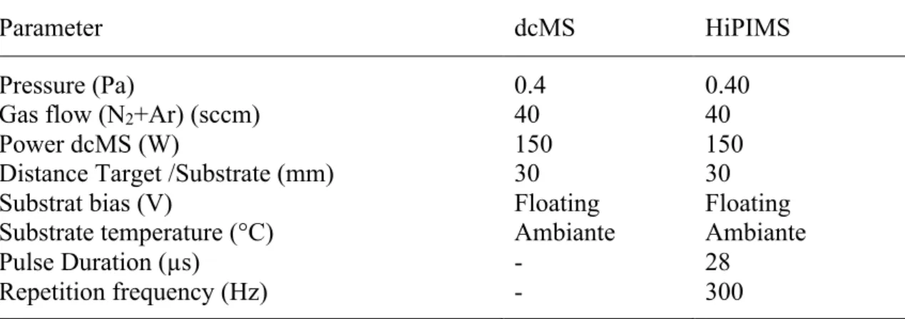
Table 1. Deposition parameters of AlN films
Parameter dcMS HiPIMS
Pressure (Pa) 0.4 0.40
Gas flow (N2+Ar) (sccm) 40 40
Power dcMS (W) 150 150
Distance Target /Substrate (mm) 30 30
Substrat bias (V) Floating Floating
Substrate temperature (°C) Ambiante Ambiante
Pulse Duration (µs) - 28
Repetition frequency (Hz) - 300
Table 2. Values of SAW properties, structural and surface parameters of epitaxial AlN buffer layer (sample (a)), AlN(dcMS)/epitaxial AlN buffer layer (sample (b)) and AlN(HiPIMS)/epitaxial AlN buffer layer ( sample (c)).
Sample (a) Sample (b) Sample (c)
Insertion Loss IL (dB) 51 53 35
Center frequency f0 (MHz) 575 586 584
SAW velocity (m/s) 13800 14064 14016
FWHM (002) –rocking curve (°) 1 1 1
Surface roughness (nm) 0.7 2 1
Figure 1. Schematic of grown sample structures.
Si(111) substrate
Epitaxial AlN buffer layer
Si(111) substrate
Epitaxial AlN buffer layer 500 nm thick of AlN
deposited by dcMS
Si(111) substrate
Epitaxial AlN buffer layer 500 nm thick of AlN deposited by HiPIMS
14 (0 02 ) AlN (HiPIMS) Epitaxial AlN buffer layer 2q (°) Cu Ka
In
te
n
si
ty
(a
rb
. u
n
its
)
(a )
Sample (c) Sample (b) 30 32 34 36 38 40 Sample (a)15
16
18
20
22
24
Sample (a) sample (b) sample (c)N
orm
ali
ze
d
int
en
si
ty (a
rb. units
)
q (°) Co K
a(b)
16 Figure 2. (a) XRD patterns of AlN thin film, (b) Rocking curve around the (002) reflection
and (c) j-scans from sample (c) around the AlN (101), epitaxial AlN buffer layer (101) and Si(220) atomic planes.
In
te
nsi
ty
(a
rb
. u
nit
s)
j (°)
AlN (HiPIMS) (101) 0 50 100 150 200 250 300 350 Si(220) Dj = 1.5° Dj = 1.5° AlN (Template) (101) (c )17 Figure 3. Room temperature Raman spectra of AlN thin films.
550
600
650
700
750
Int
en
s
it
y
R
a
m
a
n
(ar
b
. u
n
it
s)
Raman shift (cm
-1)
Sample (a)
Sample (b)
Sample (c)
Epitaxial AlN buffer layer E2(high) 649 cm-1
A1(TO)
AlN (HiPIMS) E2(high) 662 cm-1
18 Figure 4. Cross-sectional SEM images of the AlN film deposited on the epitaxial AlN buffer layer/Si(111) substrate, (a) AlN deposited by dcMS (i.e., sample (b)), (b) AlN deposited by HiPIMS (i.e., sample (c)).
200 nm Si (111)
Epitaxial AlN buffer layer
AlN (dcMS)
(a )
Si (111) 200 nm AlN (HiPIMS)(b)
19
(a)
(c)
rms = 0 .7 nm rms = 1 nm(b)
rms = 2 nm(c)
20 Figure 5. AFM images of, (a) eptitaxial AlN buffer layer (i.e., sample (a)), (b) AlN
(dcMS)/epitaxial AlN buffer layer (i.e., sample (b)) and (c) AlN (HiPIMS)/epitaxial AlN buffer (i.e., sample (c)).
Figure 6. Frequency response characteristics of fabricated SAW devices with different
configurations: IDT/epitaxial AlN buffer layer (sample (a)), IDT/AlN(dcMS)/epitaxial AlN buffer layer (sample (b)) and IDT/AlN(HiPIMS)/epitaxial AlN buffer layer (sample (c)).