Strain reduction in selectively grown CdTe by MBE on nanopatterned
silicon on insulator (SOI) substrates
R. Bommenaa,b, T. Seldrumc, L. Samainc, R. Sporkena,c, S. Sivananthana and S.R.J. Brueckd
a Microphysics Laboratory, University of Illinois at Chicago, IL b EPIR Technologies Inc., Bolingbrook, IL
c Laboratoire de Physique des Materiaux Electroniques, University of Namur, Belgium d Center for High Technology Materials, University of New Mexico, NM
Abstract
Silicon based substrates for the epitaxy of HgCdTe are an attractive low cost choice for monolithic integration of infrared detectors with mature Si technology and high yield. However, progress in heteroepitaxy of CdTe/Si (for subsequent growth of HgCdTe) is limited by the high lattice and thermal mismatch which creates a lot of strain at the heterointerface that results in high density of dislocations. Previously we have reported1 theoretical modeling of strain partitioning between CdTe and Si on nanopatterned SOI substrates. In this paper, we present an experimental study of CdTe epitaxy on nanopatterned (SOI). SOI (100) substrates were patterned with interferometric lithography and reactive ion etching to form a 2-D array of silicon pillars with ~250nm diameter and 1µm pitch. MBE was used to grow CdTe selectively on the silicon nanopillars. Selective growth of CdTe was confirmed by SEM, AFM and XPS. Coalescence of CdTe on the silicon nanoislands has been observed from the SEM characterization. Selective growth was achieved with a two step growth process involving desorption of nucleation layer followed by regrowth of CdTe at a rate of 0.2Å/s. Strain measurements by Raman spectroscopy show a lower Raman shift (2.7 ± 2 cm-1 from the bulk value of 170 cm-1 ) in CdTe grown on nanopatterned SOI compared to planar silicon (Raman shift of 4.4 ± 2 cm-1), indicating reduced strain on the nanopatterned substrates.
1 R. Bommena, C.Fulk, J. Zhao, S. Sivananthan, S.R.J. Brueck and S.D. Hersee, J .of Electron. Mater. 34,
704 (2005)
1. Introduction
The ability to integrate together highly lattice –mismatched materials can open up a multitude of possibilities for device engineers. Heteroepitaxy process enables the development of new materials, which lack a bulk growth technology. One such material is CdTe, which is an important semiconductor material, which forms an alternative substrate for the growth of HgCdTe: the most commonly used material for the production of infrared focal plane arrays. Technical difficulties in the bulk growth of high quality, large area CdTe necessitates the heteroepitaxy process of CdTe. Several substrates have been explored for the epitaxy of CdTe namely InSb2, Sapphire3, GaAs4 and Silicon5.
Among these substrates Si is the attractive choice because
(a) Si wafers are available in large areas and large quantities at an inexpensive price
(b) Si wafers have excellent mechanical properties
(c) Infrastructure for fabrication of silicon based integrated circuits has been well established
Despite all the advantages that the silicon substrates offer, CdTe/Si material system faces several difficulties: large lattice mismatch of 19% between CdTe and Si which results in a lot of strain at the heterointerface, a high thermal mismatch which supplements the strain when the epilayer is cooled from the growth temperature.
There are two major issues that must be addressed when considering heteroepitaxy: lattice mismatch and thermal mismatch. Lattice mismatch epitaxy is a situation where two materials featuring different lattice constants are brought together by deposition of one material on top of the other. If this mismatch is high then dislocations are created to accommodate stress. The layer thickness at which dislocations occur is referred to as the critical layer thickness. It is desirable to extend the critical thickness in a heteroepitaxial system. Dislocations are usually created at the heterointerface and they may include: screw dislocations, misfit dislocations and threading defects. The threading defects are particularly problematic as they propagate into the epilayer and are known to reduce device performance and reliability.
2. R. F. C. Farrow, G. R. Jones, G. M. Williams, and I. M. Young, Appl. Phys. Lett. 39 (1981). 3 . T.H. Myers, Y. Lo, R.N. Bicknell, J.F. Schetzina, Appl. Phys. Lett. 42 (1983).
4 . H.C. Jeon, J. H. Leem , Y.S. Ryu , Appl. Surf. Sci. 156 (2000).
Thermal mismatch arises from the difference in thermal expansion co-efficients between the substrate and the epilayer. Typically this is seen after growth when the sample is cooled from growth temperature to room temperature. Strain and cracks can form in the epilayer or the substrate due to the thermal mismatch and this is problematic because macroscopic areas of crack free material are necessary for device fabrication. Thus, thermal mismatch in a heteroepitaxial system is also a major issue while selecting a suitable substrate. Satisfying these conditions for heteroepitaxy is not trivial and it is often difficult to grow a heteroepitaxial film of high quality with a smooth surface free from cracks and dislocations6.
In the case of planar heteroepitaxy, strain in the material system is usually relaxed in two dimensions and the strain energy, which is a function of the square of the strain, increases linearly with the epilayer thickness. Alternatively, novel 3-dimensional strain relaxation mechanisms are available by reducing the lateral dimensions of the substrate to nanoscale. This technique known as Nanoheteroepitaxy (NHE)7 has been developed for heterogeneous integration of lattice mismatch systems. Our Previous work89 on this approach in GaN/Si (lattice mismatch of 21%) material system has been successful in the reduction of strain in the material system.
Theory of CdTe/Si strain partitioning
Strain in planar CdTe heteroepitaxy is almost completely experienced by the CdTe epilayer in the process of registering its lattice on the substrate. This constrains the epilayer to accommodate the total strain in the material system thereby subjecting it to tensile strain or compressive strain depending on the lattice mismatch between the substrate and the epilayer.
Nanoheteroepitaxy integrates a compliant substrate10 approach (which predicts strain partitioning between epilayer and substrate) and a defect reduction theory proposed by Luryi and Suhir11 (interface dislocation density is reduced when substrate dimensions are reduced to nanoscale) to result in 3-dimensional strain relaxation mechanisms in
6 . W. M . Yam and R. J. Paff, J. Appl. Phys., 45, 1456 (1974). 7 . D. Zubia and S.D. Hersee, J. Appl. Phys., 85, 6492 (1999).
8. R. Bommena, C. Fulk, J. Zhao, T.S.Lee, S. Sivananthan, S.R.J. Brueck and S.D.Hersee, J .Electron.
Mater. 34, 704 (2005)
9 . X. Sun, R. Bommena, D. Burckel, S.D. Hersee and S.R.J. Brueck, J. of Appl. Phys. 95 (2004). 10 Y. H. Lo, Appl. Phys. Lett. 59, 2311 (1991)
11 S. Luryi, E. Suhir , “New approach to the high quality epitaxial growth of lattice mismatched materials,”
nanoscale patterned compliant substrates.
Strain partitioning between CdTe and Si has been modeled in our previous work8 based on the theoretical predictions of nanoheteroepitaxy. Strain partitioning between CdTe and Si was simulated using nanopatterned silicon on insulator (SOI) substrates with a 20nm thick top silicon layer. We present the experimental work done on this approach using nanopatterned SOI substrates in this paper.
2. Experimental Procedure
The process flow for the experimental work of nanoheteroepitaxy of CdTe consists of fabrication of nanoscale compliant silicon substrates followed by selective growth of CdTe on these substrates. Fabrication of the nanoscale substrates was performed by interferometric lithography and reactive ion etching while the selective growth of CdTe on these substrates was performed by MBE growth technique.
Silicon on insulator substrates (SOI) (100) substrates obtained from SOITEC, France with a 20nm thick silicon layer/143nm silicon dioxide layer/handle silicon substrate were used for fabrication of nanopatterned substrates. A scalable and inexpensive lithographic technique is required for generating periodic nanoscale features over large area wafers and this requirement was fulfilled by interferometric lithography (IL). Interferometric lithography is a mask-less and relatively simple method of forming periodic arrays12 of sub-micron structures on the surface of a substrate that uses interference between coherent laser beams to define a pattern. There is a large parameter space that needs to be explored when fabricating nanoscale features: the feature density and dimensions, pattern symmetry, the underlying layer structure and also the grouping of the nanoelements. Interferometric lithography is a unique approach that in principle allows all these requirements13 to be controlled.
SOI substrates (20mm x 20mm pieces) were subjected to a chemical rinse in piranha (5H2SO4: 1H2O2) and then deionized water. A layer of antireflective coating
(ARC) XHRI-16 was spun on the samples at 4000rpm for 30 seconds and then hard baked at a temperature of 1750C for 3 minutes. ARC is an organic polymer that serves to avoid standing wave patterns that would otherwise result from the interference between the incident laser beam and the reflected beam from the substrate. A layer of positive photoresist was spun on these samples at 3000rpm for 30 seconds and baked at 950C for
12 S.H.Zaidi, A.S.Chu and S.R.J.Brueck, J. Appl. Phys. 80, 6997 (1996)
13 S.R.J.Brueck , “Interferometric lithography –From periodic arrays to arbitrary structures,” in
60 seconds. The samples were exposed on the IL setup for 15 sec and then rotated by 90◦ for a second exposure to obtain 2-dimensional features. Following the UV exposure, samples were developed in a MF702 developer for 75 seconds. The principle of pattern generation on the IL setup is governed by Bragg’s law:
λ = 2d sin (θ)
Where λ = wavelength of the incident radiation (355nm) d = density / pitch of the grating
2θ = angle between the two incident beams
Following the interferometric lithography process, reactive ion etching with CHF3 and O2
as precursors was used to transfer the nanoscale patterns into the silicon layer.
MBE growth of CdTe was then performed on these nanopatterned substrates and planar silicon substrates for a direct comparison. MBE growth process was performed on an OPUS 45 chamber, which has the capability to grow on 5-inch silicon wafers. The chamber consists of three interconnected vacuum chambers: (a) introduction chamber (b) preparation chamber and the (c) growth chamber. The introduction chamber is equipped with wafer –handling assembly which can handle up to ten substrate holders. The substrate holders are 5-inch diameter platen, made of molybdenum with 2-inch, 3-inch or 4-inch diameter hole in the center suitable for corresponding size wafers to be placed on them. A custom holder suitable to hold 6 pieces of 10mm x 10mm and 2 pieces of 20mm x 20mm was used for the CdTe growth on nanopatterned SOI substrates. Samples were subjected to an ex-situ cleaning process involving piranha clean for 5 minutes followed by a buffered oxide etch (3[7NH4F: 1HF]: 1NH4OH) for 10 seconds. These were rinsed
in deionized water for 5 minutes and blown dry with nitrogen. Following the ex-situ cleaning process, samples were loaded into the introduction chamber and then transferred into the preparation chamber in vacuum, where they were prebaked at about 500°C for 8 hrs. The samples were then transferred into the growth chamber under high vacuum and the temperature was ramped to 950°C. The samples were left at that temperature for duration of 10 minutes to desorb the oxide on the silicon surface. The samples were subjected to an arsenic flux while ramping down the temperature to 400°C. A CdTe nucleation layer was deposited for 5 minutes at 310°C. An epilayer was then grown at 330°C on one sample. On a couple of other nanopatterned samples, the as grown nucleation layers were desorbed at 600°C and the epilayers were grown at 330°C for 900seconds and 3600 seconds. The as grown samples were characterized by SEM, AFM and XPS. Strain characterization was performed by Raman scattering measurements in a
backscattering geometry using a Renishaw micro –Raman system (1800 cm-1 to 1 cm-1 ). A spatial resolution of ~ 1µm was obtained with a 100X objective lens on this system.
3. Results and Discussions
Two –dimensional pillars in photoresist were obtained from the interferometric lithography process with feature dimensions between 200nm to 350nm as shown by the scanning electron microscope images in Figure 1.
Figure 1: SEM images of nanoscale photoresist pillars on SOI substrates fabricated with interferometric lithography
Scanning electron microscope images of the reactive ion etched samples are shown in Figure 2. The diameter of the silicon islands obtained after the etch process were in the range 150nm-250nm on different pitch between 360nm-1000nm. Clean surface of the etched silicon region exposing the silicon dioxide layer can be seen from the SEM images.
a. b.
Silicon SiO2
Figure 2: (a) ~ 150 nm Silicon nanopillars on 360nm pitch (b) ~ 200nm Silicon nanopillars on 500nm pitch (c) ~250nm silicon nanopillars on 1000nm pitch (e) Cross-sectional SEM view of silicon nanopillars on 500nm pitch
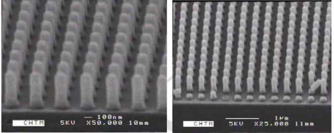
Scanning electron microscope images of CdTe epilayer grown without the desorption of the nucleation layer is shown in Figure 3 (a) while images of CdTe grown with desorption of the initial CdTe layer are shown in Figure 3(b) (c) and (d).
Figure 3: (a) CdTe growth from conventional growth process (b) Selective CdTe growth after 900sec of growth (c) Selective CdTe after 3600sec of growth (d) Angular view SEM of selective CdTe after 3600 sec
c. d.
a. b.
c. d.
CdTe growth –no selectivity
Selective CdTe Selective CdTe SiO2 5µm 5µm 5µm
With the conventional growth process we observe that CdTe growth is not selective on the silicon islands (figure 5 (a)) from the SEM images. Polycrystalline CdTe is seen between the silicon islands which indicate the nucleation of CdTe on the amorphous silicon dioxide between the nanoislands of silicon. In the case of the CdTe grown with the desorbed nucleation layer we observe the nucleation of CdTe only on the silicon islands and no nuclei of CdTe are found on the silicon dioxide. It can be explained hypothetically that the high temperature process at 600°C desorbs the CdTe deposited on the silicon islands and the polycrystalline material deposited on the silicon dioxide growth mask. However, since the bond energy between silicon and Te is higher compared to silicon dioxide and Te, all the polycrystalline material deposited on the silicon dioxide mask is desorbed at this temperature while few Te atoms are still bonded to the silicon surface on the nanopillars. When epilayer growth is subsequently performed, CdTe grows on top of the silicon islands resulting in selective growth of CdTe.
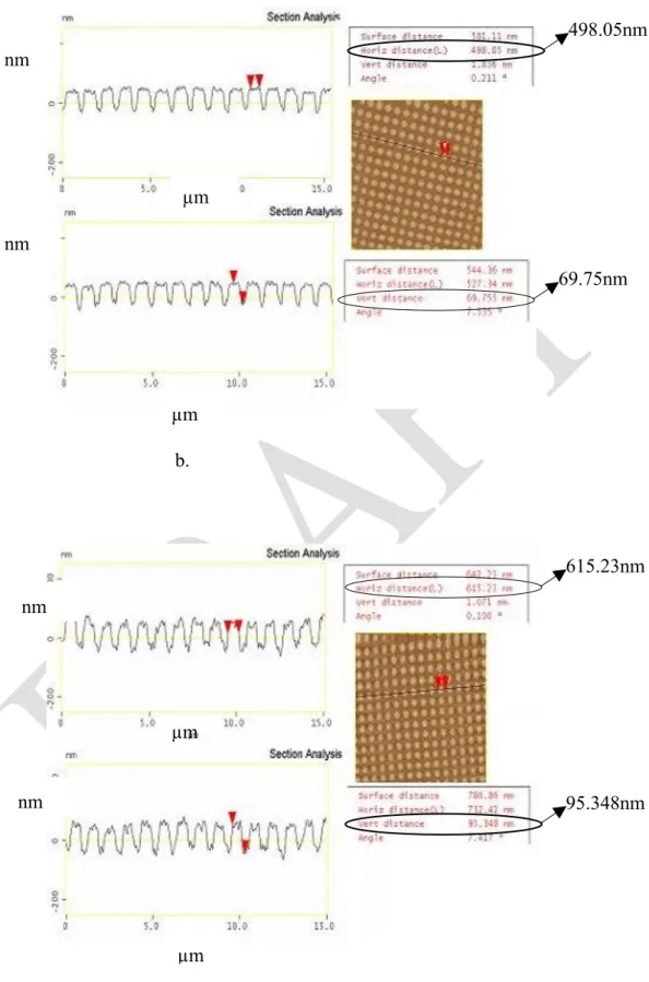
Atomic force microscopy (AFM) images of the nanopatterned substrate and the CdTe epilayers grown on these substrates with the section analysis performed are shown in Figure 4 (a), (b) and (c).
a. µm µm nm nm 292.97nm 37.85nm
Figure 4: (a) AFM section analysis of nanopatterned SOI substrate (b) AFM analysis of selective CdTe grown for 900sec (c) AFM analysis of selective CdTe grown for 3600 sec
b. µm nm µm nm 498.05nm 69.75nm c. nm µm nm µm 615.23nm 95.348nm
The following data is evaluated from the AFM analysis
Lateral dimension Vertical dimension
Nanopatterned substrate 292nm 37nm
Selective CdTe (900 sec) 498nm 69nm
Selective CdTe (3600 sec) 615nm 95nm
The vertical dimension of the silicon nanopillar on the substrate which is indicative of the thickness of the silicon island is ~37nm. This is due to the over etching (~17nm into the silicon-dioxide) in the pattern transfer process with reactive ion etch because the chemistry used also etches silicon dioxide. The lateral growth rate of CdTe on the silicon islands is between 0.8-2.0Å/s while the vertical growth rate is between 0.1-0.3 Å/s which indicates a higher lateral growth rate versus vertical growth rate. This is probably due to the high surface area of the silicon nanoislands compared to the height that enhances the nucleation and growth of CdTe laterally. However, a clearly defined step shown by the AFM profile between the CdTe grown on the silicon nanopillars and the underlying silicon dioxide mask indicates that CdTe is growing selectively on the silicon islands.
Selectivity of CdTe was further confirmed by the XPS scan shown in the figure 5.
Figure 5: XPS Spectrum of selective CdTe on silicon nanopillars
XPS spectrum from figure 5 shows the photoemission peaks from the different elements present on the selective CdTe/Si sample. The emission from the Si 2p core levels from
the survey scan across the sample indicate that the CdTe grown is selective (the silicon peaks would not be seen if there was CdTe deposition everywhere on the sample).
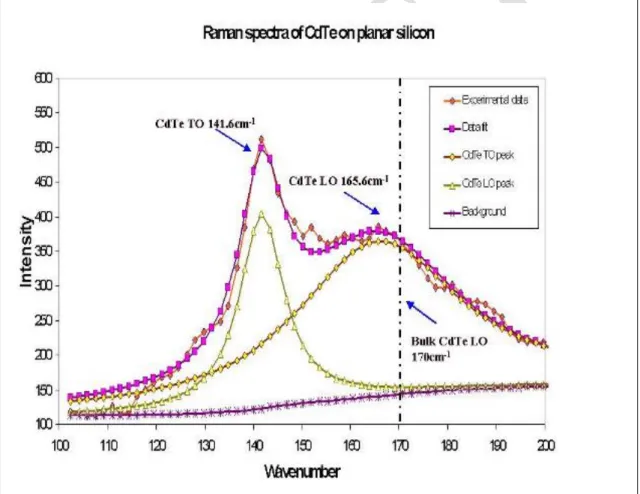
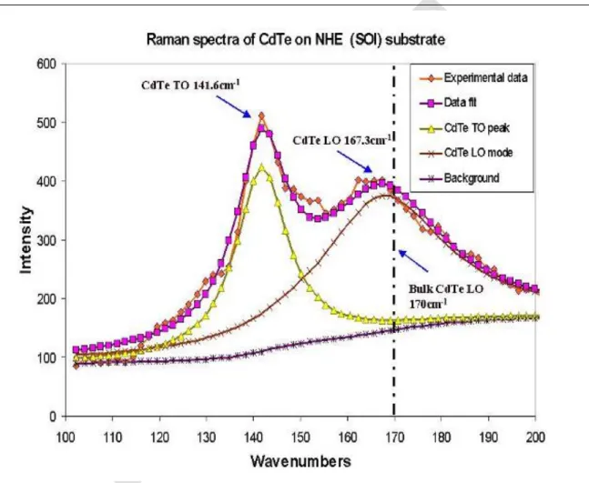
Strain characterization was performed on epitaxial CdTe grown on planar silicon and nanopatterned compliant SOI substrates using Raman spectroscopy. Raman spectroscopy is a non –invasive technique for monitoring strain in heteroepitaxial systems14,15,16,17. CdTe has a Raman active transverse optical (TO) and a longitudinal optical mode (LO). The LO mode of the CdTe for unstrained bulk material is reported be 170cm-1 and this phonon peak translates with strain to higher wavenumbers for compressive strain and lower for tensile strain. The TO mode of CdTe is reported to be around 141 cm-1 and has not been reported to be affected by strain. Raman spectra of CdTe grown on planar silicon and nanopatterned SOI are shown in Figure 6 and Figure 7.
Figure 6: Raman spectra of CdTe grown on planar silicon
A fitting program has been used to fit the experimental data obtained from the Raman
14 . P. M. Amirtharaj and F. Pollak, Appl. Phys. Lett. 45 (1984). 15 . W. J. Meng, T. A. Perry , J. of. Appl. Phys., 76(12), 7824 (1994). 16 . D. Kirillov, H. Lee, J.S. Harris, J.of Appl. Phys., 80(7), 4058 (1996).
spectroscopy on CdTe grown on nanopatterned SOI and planar silicon substrates. The Raman spectra obtained from the epitaxial CdTe on planar silicon shows a Raman shift of ~4.4 ± 2cm-1 from the bulk value of 170 cm-1 as shown in Figure 6. The spectra obtained on the CdTe grown on the nanopatterned SOI substrates shows a Raman shift of ~2.7 ± 2 cm-1 from the bulk value as shown in Figure 7. The lower shift obtained on the nanopatterned substrates is due to the additional strain relaxation mechanism provided by the nanoscale size and the compliance of the substrate.
Figure 7: Raman spectra of selective CdTe grown on nanopatterned SOI substrate
4. Conclusions
Interferometric lithography and reactive ion etching have been successfully used to fabricate nanopatterned silicon on insulator substrates to explore the experimental feasibility of the previously developed theoretical model for nanoheteroepitaxy of CdTe. Selective growth of CdTe on silicon nanoislands has been successfully achieved with MBE technique for the first time as confirmed from the SEM, AFM and the XPS measurements. Raman strain characterization of the epitaxially grown CdTe on planar
silicon substrates and nanopatterned SOI substrates shows lower strain on nanopatterned substrates, indicative of strain relaxation mechanism provided by the nanopillars. Further work in achieving lateral epitaxial overgrowth and coalescence of CdTe on nanopatterned substrates should provide a pathway for growing high quality HgCdTe epilayers.