UNIVERSITÉ DE MONTRÉAL
HIGH-DENSITY 3D PYRAMID-SHAPED MICROELECTRODE ARRAYS FOR BRAIN-MACHINE INTERFACE APPLICATIONS
BAHAREH GHANE MOTLAGH INSTITUT DE GÉNIE BIOMÉDICAL ÉCOLE POLYTECHNIQUE DE MONTRÉAL
THÈSE PRÉSENTÉE EN VUE DE L’OBTENTION DU DIPLÔME DE PHILOSOPHIAE DOCTOR
(GÉNIE BIOMÉDICAL) NOVEMBRE 2015
UNIVERSITÉ DE MONTRÉAL
ÉCOLE POLYTECHNIQUE DE MONTRÉAL
Cette thèse intitulée :
HIGH-DENSITY 3D PYRAMID-SHAPED MICROELECTRODE ARRAYS FOR BRAIN-MACHINE INTERFACE APPLICATIONS
présentée par : GHANE MOTLAGH Bahareh
en vue de l’obtention du diplôme de : Philosophiae Doctor a été dûment acceptée par le jury d’examen constitué de :
M. SAVARD Pierre, Ph. D., président
M. SAWAN Mohamad, Ph. D., membre et directeur de recherche M. SAVADOGO Oumarou, D. d'état, membre
DEDICATION
To Kianoush & My parents…
ACKNOWLEDGEMENTS
The completion of this dissertation has been an amazing journey filled with many experience from the labs to the real life!
I had the opportunity to work under the supervision of truly astonishing individual Prof. Mohamad Sawan. Thank you for accepting me into your scientific group and providing me your guidance and support. There have been several occasions where I remember feeling discouraged and skeptical about the path that I am taking but a meeting with you has refreshed my enthusiasm and raised my courage infinitely. Your dedicated support and guidance have been outstanding over the past five years and it has been a privilege to work under your supervision. I would like to express my gratitude to Prof. Richard Martel and Prof. Kevin J. Wilkinson for their precious advice and contribution to this research and thesis. Thank you for kindly granting your time and answering many of my questions.
I gratefully appreciate the time of my dissertation committee members, Prof. Pierre Savard, Prof. Oumarou Savadogo, and Prof. Rolf Wüthrich to read this thesis and to help me move this forward. Their questions and comments certainly helped to improve my thesis.
I would like to thank my research mates and collaborators, May Choueib, Alireza H. Mesgar, Taraneh Javanbakht, Amal Kassab, Md Hasanuzzaman, and Ehsan Kamrani for offering their expertise and advice along this project.
I would like to gratefully acknowledge the help of Christophe Clément and Laurent Mouden for technical support in cleanroom, LASEM, and Biostim. The work has not been completed without the technical team that keeps everything working. Thank you for so generously providing me with your assistance and time. My sincere thanks to Marie-Hélèn Bernier and Richard Vernhes for providing their expertise in micro/nanofabrication and characterizing my sample.
The past several years have not been an easy ride and I realized the importance of family and friends to completion of a project of this magnitude. I am extremely fortunate to have a support group of my friends to encourage me and make a strong interest in my continued development and growth.
Last but not least, I am grateful to my parents for their unconditional love and continued support. I would not have made it this far without them. Special thanks to my beloved Kianoush, without whose endless love and moral support, this task could have never been completed.
RÉSUMÉ
Les dispositifs médicaux dédiés aux enregistrements des activités neuronales et à la stimulation de tissus nerveux sont appelés interfaces cerveau-machines. Ils offrent un potentiel important pour restaurer diverses fonctions neurologiques perdues. Un élément clé dans la mise en œuvre des dispositifs est le réseau de microélectrodes (MEAs pour MicroElectrode Arrays en anglais) servant d’interface avec les tissus nerveux. Les MEA jouent un rôle important dans les implants lors d’expérimentations chroniques, ils doivent être fiables, stables et efficaces pour l'enregistrement et la stimulation à long terme. Les propriétés électrochimiques et la compatibilité biologique des microélectrodes sont des facteurs essentiels qui doivent être prises en compte lors de leur conception et fabrication.
La présente thèse traite de la conception et la fabrication de MEA en silicium micro-usiné à haute densité et en forme de pyramides qui sont destinés à l’enregistrement et la stimulation intracorticals 3D. Nous nous concentrons principalement sur les techniques de microfabrication des électrodes et le développement de procédure du revêtement de matériaux nécessaires pour la biocompatibilité et protection des dispositifs implantables. Nous élaborons des microélectrodes à hauteur variable pour enregistrer des signaux neuronaux, sans perdre la capacité de microstimulation et tout en maintenant des impédances de faibles valeurs. Cette caractéristique est obtenue en modifiant la géométrie et la composition de matériaux utilisés, ce qui facilite l'injection de charge et la résolution spatiale élevée.
Nous présentons une nouvelle technique de micro-usinage 3D à nombre réduit de masques comparé aux techniques existantes. Nous décrivons la mise en œuvre d’un MEA à haute densité (25 électrodes / 1,96 mm2) et à différentes longueurs d’électrodes. En outre, une nouvelle technique de masquage à base de film sec a été développée pour obtenir de très petites surfaces actives pour les microélectrodes qui sont à hauteur variable. Nous avons réduit les étapes du procédé de masquage de 14 à 6 par rapport à la méthode classique de masquage utilisé dans la littérature. Nous avons ensuite effectué, pour la première fois, une croissance directe sélective de nanotubes de carbone sur les têtes de microélectrodes de longueurs variables en utilisant la technique du dépôt chimique en phase vapeur assisté par plasma (Plasma-Enhanced Chemical Vapor Deposition - PECVD). Ce recouvrement a amélioré les propriétés électriques des
électrodes de façon significative. En effet, ce revêtement par des nanotubes de carbone a impliqué une diminution d’un facteur 5 de l'impédance et une augmentation de 600 fois le transfert de charges par rapport à une électrode de Platine. Enfin, nous avons mis en évidence par des tests de cellules de culture in vitro, l'importance de revêtement des MEA avec des molécules bioactives (Poly-D-lysine) et de polyéthylène glycol hydrogels pour minimiser la réponse immunitaire du tissu neuronal aux MEA implantés.
ABSTRACT
Neuroprosthetic devices that can record neural activities and stimulate the central nervous system (CNS), called brain-machine interfaces (BMI), offer significant potential to restore various lost neurologic functions. A key element in functions restoration is Microelectrode arrays (MEAs) implanted in neural tissues. MEAs, which act as an interface between bioelectronic devices and neural tissues, play an important role in chronic implants and must be reliable, stable, and efficient for long-term recording and stimulation. Electrochemical properties and biological compatibility of chronic microelectrodes are essential factors that must be taken into account in their design and fabrication.
The present thesis deals with the design and fabrication of silicon micromachined, high-density, pyramid-shaped neural MEAs for intracortical 3D recording and stimulation. The focused is mainly on the MEAs fabrication techniques and development of coating materials process required with implantable devices with an ultimate purpose: elaborate variable-height microelectrodes to obtain consistent recording signals from small groups of neurons without losing microstimulation capabilities, while maintaining low-impedance pathways for charge injection, high charge transfer, and high-spatial resolution by altering the geometries and material compositions of the array.
In the first part of the thesis, we present a new 3D micromachining technique with a single masking step in a time and cost effective manner. A high density 25 electrodes/ 1.96 mm2 MEA with varying lengths electrodes to access neurons that are located in different depths of cortical tissue was designed and fabricated. Furthermore, a novel dry-film based masking technique for procuring extremely small active area for variable-height electrodes has been developed. With this technology, we have reduced the masking process steps from 14 to 6 compared to the conventional masking method. We have then reported for the first time a selective direct growth of carbon nanotubes (CNTs) on the tips of 3D MEAs using Plasma Enhanced Chemical Vapor Deposition (PECVD) that could enhance electrical properties of the electrodes significantly. The CNT coating led to a 5-fold decrease in impedance and a 600-fold increase in charge transfer compared with Pt electrode. Finally, we have highlighted the importance of the coating MEAs with bioactive molecules (Poly-D-lysine) and polyethylene glycol (PEG) hydrogels to minimize the immune response of the neural tissue to implanted MEAs by in vitro cell-culture tests.
TABLE OF CONTENTS
DEDICATION ... iii
ACKNOWLEDGEMENTS ... iv
RÉSUMÉ ... vi
ABSTRACT ... viii
LIST OF TABLES ... xii
LIST OF FIGURES ... xiii
LIST OF ABBREVIATIONS ... xix
CHAPTER 1 INTRODUCTION ... 1
1.1 Scope of the thesis ... 1
1.2 The advent of penetrating Microelectrode arrays (MEA) ... 1
1.3 Current challenges ... 2
1.4 Microelectrode arrays: a key element in neuroprosthetic devices ... 4
1.5 Objectives of the present work ... 5
1.6 Specifications of projected MEAs ... 6
1.7 Summary of contributions ... 7
1.8 Organization of the thesis ... 8
1.9 Publications ... 9
CHAPTER 2 OVERVIEW OF IMPLANTABLE MICROELECTRODE ARRAYS ... 11
2.1 Introduction to neural MEAs ... 11
2.2 Properties of MEAs ... 13
2.3 Application of penetrating MEAs ... 14
2.4 Fabrication technologies of penetrating MEAs... 15
2.4.1 Traditional Microelectrode arrays ... 16
2.4.2 Microwires ... 18
2.4.3 Micromachined MEAs ... 20
2.4.4 Other approaches to MEAs fabrication ... 26
2.5 Comparison of penetrating microelectrodes technologies ... 30
2.6 Planar microelectrode arrays (pMEA) ... 33
2.7.1 Material science strategies ... 37
2.7.2 Bioactive molecule strategies ... 38
2.8 Electrical circuit model of MEAs ... 40
2.9 Perspective of the work in this thesis ... 42
CHAPTER 3 EXPERIMENTAL PROCEDURES OF MEAs’ PREPARATION ... 44
3.1 Design and fabrication of neural 3D MEAs using micromachining techniques ... 44
3.1.1 MEAs backside fabrication process ... 44
3.1.2 MEAs frontside fabrication process ... 46
3.1.3 Shank insulation ... 50
3.1.4 Masking process to de-insulate active sites of the electrodes ... 51
3.1.5 Electrodes tip-coating ... 52
3.1.6 Tip-metallization and lift-off ... 53
3.1.7 CNTs tip-coating ... 54
3.2 Characterization of the neural MEAs ... 56
3.2.1 Scanning electron microscopy (SEM) imaging ... 57
3.2.2 Energy-dispersive X-ray spectroscopy (EDX) analysis ... 57
3.2.3 Electrochemical characterization; Electrochemical impedance spectroscopy (EIS), Cyclic voltammetry (CV), and Charge injection capacity (Qinj) ... 58
3.3 Results and discussion ... 59
3.3.1 Fabrication of 3D MEAs ... 59
3.3.2 Masking process ... 61
3.3.3 Tip-metal deposition ... 61
3.3.4 Tip-CNTs Growth ... 62
3.3.5 Tip-CNTs deposition (Coffee stains technique) ... 64
3.3.6 MEAs Electrical Properties ... 65
3.3.7 Equivalent circuit model ... 68
3.4 Discussions ... 72
3.5 Conclusion ... 74
CHAPTER 4 BIOCOMPATIBILITY OF MEAs ... 75
4.1 Bioactive molecule deposition ... 75
4.1.1 MEAs preparation ... 76
4.1.3 Conjugation of peptide (poly-D-lysine) to the MEAs ... 78
4.1.4 Fourier transform infrared spectroscopy (FTIR) analysis ... 79
4.2 Cell cultures and in vitro cell test ... 79
4.2.1 Culture neuroblast cell line (CCL-131) ... 79
4.2.2 Cell-counting ... 79
4.2.3 Cell incubation with the electrodes before and after PDL coating ... 80
4.2.4 Statistical analysis ... 80
4.3 Results ... 80
4.3.1 Conjugation of PDL and PEG to the MEAs ... 80
4.3.2 Conjugation of peptides to MEAs ... 81
4.3.3 FTIR analysis ... 82
4.3.4 Effect of polymer coating on the cell size, morphology, and proliferation ... 85
4.3.5 Cell proliferation on the peptide-conjugated MEAs ... 86
4.4 Discussion ... 90
4.5 Conclusion ... 91
CHAPTER 5 CONCLUSION, GENERAL DISCUSSION, AND PERSPECTIVES ... 93
5.1 Summary of the results and contributions ... 93
5.2 Perspectives for future work ... 96
LIST OF TABLES
Table 2.1. Advantages and drawbacks of MEAs fabrication methods [1-4]……….……31
Table 2.2. Characterization of MEAs technologies [5, 6]……….32
Table 2.3. Comparison of microelectrodes structure [7-10]……….……….32
Table 2.4. Impedance of the poly-silicon electrode before and after CNTs deposition [11]….…35 Table 2.5. Measured impedance of electrodes with diameter of 40 µm as a function of gold nanopillar height [12]……….36 Table 3. 1. Comparison of conventional and proposed masking processes……….…...53
Table 3. 2. Sputtered deposition parameters for the electrodes’ tip-metallization………….….…54
Table 3.3. Average impedance of different electrode-tip coatings……….……67 Table 3. 4. Fitting results from the EIS model……….…...69
Table 3. 5. Comparison of neural Microelectrode arrays……….……..71 Table 4. 1. Sputtered deposition parameters for the electrodes’ tip-metallization……….…….…77 Table 4. 2. The number of cells per electrode site for each tip coating before and after PDL coating………88
LIST OF FIGURES
Figure 1.1. Schematic view of a silicon micromachined neural MEA with variable heights of 1.45, 1.55, and 1.65 mm. The shank was covered with parylene-C (and PEG) and the active sites of each array were coated with Pt, sputtered iridium oxide (SIRO), or CNTs. The thickness of the electrodes was 200 μm at the base and about 2 μm at the tip with 100 μm spacing………...……….………..…7 Figure 2.1. Implanted microelectrode in the cortex. Neural stimulation occurs via current passes through the tip to the surrounding neurons. Reprinted with permission from Ref. [13]………...………...…...15 Figure 2.2. Scanning electron microscopy (SEM) images of Glass insulation and the metal part
(Pt) of the metal-wire electrode. Reprinted with permission from Ref. [14]……….16
Figure 2.3. SEM (top) and Optical microscopy images of pre-processed and conventionally processed glass pipettes. Reprinted with permission from Ref. [15]……….17
Figure 2.4. Microwires: (a) Wire microelectrodes embedded in ceramic substrate. The anchors ensure that the array stay in the brain, (b) Ceramic well-structure connected to parylene-C insulated gold wires. Electrodes are inserted perpendicular into the substrate, (c) SEM image of microwire insulated with 3 µm parylene-C except at the tip. Reprinted with permission from Ref. [16]……….18 Figure 2.5. SEM images of metal microelectrodes coated with CNTs: (a) CNTs covalently attached to the tungsten electrode, (b) CNTs were electrochemically deposited at the recording sites of the electrode. Reprinted with permission from Ref. [17]………..19 Figure 2.6. Michigan MEA: (a) Basic structure of a multisite microprobe presenting the substrate, insulation layers, and recording sites, (b) SEM image of the tip of neural microelectrode. Reprinted with permission from Ref. [18]………...21
Figure 2.7. Typical Michigan array: (a) A prototype of the array, consisting of 64 sites on 200 µm centers with 1640 µm width and 4 mm long shanks. The interface is shown with the 1 mm × 1 mm × 0.5 mm base resting on a penny, (b) General schematic of the four-shank electrodes forming 16-channels probe. Reprinted with permission from Ref. [19]……….21
Figure 2.8. Flexible multi-channel MEAs: (a) 3D flexible MEAs after folding, (b) Each probe with 3 recording sites. Reprinted with permission from Ref. [20]………...……….………..23 Figure 2.9. Flexible MEA: (a) A magnified photo of the 4×4 electrode array, (b) SEM image of the grown CNTs, (c) High-resolution transmission electron microscopy (HRTEM) image of the grown CNTs. Reprinted with permission from Ref. [21]………...23 Figure 2.10. SOI-based probe: (a) Schematic of the probe structure, (b) SEM image of a probe tip. The thickness of the interconnect lines is 1 µm, (c) SEM image of the 1 µm × 1 µm iridium recording site. Reprinted with permission from Ref. [22]………..24 Figure 2.11. Utah silicon-based MEAs: (a) 2D flat electrode array; (b) Slanted electrode array. Reprinted with permission from Ref. [23]………..25 Figure 2.12. Metal-based MEAs using EDM technique: (a) SEM image of a parylene-coated assembly, consisting of Pt-coated electrode tips, (b) Stainless steel electrode arrays after electrochemical polishing. Reprinted with permission from Ref. [24, 25]………26 Figure 2.13. Patch clamp recording form the neuron cell. In the cell-attached configuration, the patch electrode is sealed to the surface of the intact cell allowing channel activity in the patch of membrane under the electrode tip. Reprinted with permission from Ref. [26]……….27 Figure 2.14. The wire probe on Si (111) with W wiring circuit: (a) SEM image of silicon-wire probe combined with wring process for on-chip circuits on same a silicon wafer, (b) Silicon probe in 30 µm in length and 2 µm in diameter at a growth temperature of 600 ºC for 30 min, (c) 2 × 2 array of selective silicon-wire probes with 160 µm in length and 3.5 µm diameter at tips. The VLS growth was performed at 700 ºC for 2 h. Reprinted with permission from Ref. [27]……….28 Figure 2.15. Combination of ion-channel on a transistor: (a) HEK293 cells with a hSlo potassium channel on a silicon chip with a linear array of transistors. The cells appear in the color of the florescence of GFP, (b) Nerve cells from the leech on the open gate oxide of a field-effect transistor. The n-type silicon chip are shown in dark, the p-doped sources and drains are bright. The gates with the length of 1.8 µm and the width of 20 µm show no contract. The cell was injected using a glass capillary. Reprinted with permission from Ref. [28]………...……...29 Figure 2.16. Neuronal network on silicon chip: (a) SEM image of a two-way contact with the pins of polyimide. St (stimulator wings) and transistor (S: source, D: drain, G: gate), (b) SEM
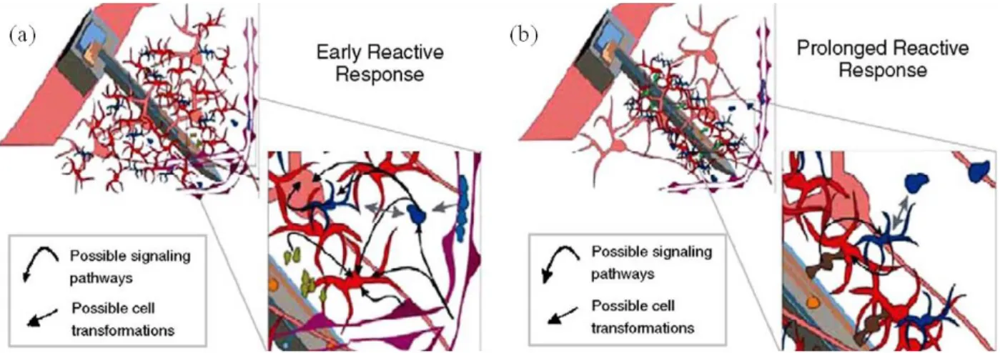
image of immobilized neurons form the pond snail after three days in culture, (c) SEM of a neuronal network with the cell bodies on a double circle of two-ways contacts after two days in culture. Reprinted with permission from Ref. [28]………...……….………30 Figure 2.17. SEM images of planar microelectrode array with 60 individual CNT electrodes. Circuit paths are insulated with 100 nm silicon dioxide layer: (a) Top view of the planar microelectrode array showing the 60 individual electrodes, (b-d) Different magnification of vertical CNT electrode network and a single CNT electrode. Reprinted with permission from Ref. [11]……….33 Figure 2.18. Process flow of microelectrodes fabrication with vertically aligned CNT networks: (a) Deposition of poly-silicon on silicon dioxide by photolithography and dry reactive ion etching, (b) Insulation electrodes and circuit path with a thermal oxide layer using dry thermal oxidation, (c) Resist spin coating and photolithography, (d) Hydrofluoric etching to open the electrode sites, (e) Aluminum and iron deposition that works as catalysts, (f) Remove the resist, (g) Direct CVD growth of vertically aligned CNTs. Reprinted with permission from Ref. [11]………...………..34 Figure 2.19. SEM images of planar microelectrodes with gold nanopillars onto the recording sites: (a-c) Top-view of planar microelectrodes with different magnification. Gold nanopillars appear dark, (d) nanostructure of goldpillars with a diameter of 200 nm and the height of 22.5 µm. Reprinted with permission from Ref. [12]……….36 Figure 2.20. Microelectrodes with different size, shape and cross-section that produced the same foreign body response and glial scar. SEM images of electrode prepared by (a) KOH etching, (b) RIE, (c) Center for Neural Communication Technology (CNCT) device. Reprinted with permission from Ref. [29]………..37 Figure 2.21. Possible mechanisms of biological responses to an implant: (a) Early reactive response in 1-3 weeks, (b) Prolonged reactive response in 6-8 weeks post implantation. Neurons are pink, astrocytes are red, microglial are blue, and vasculatures are purple. Reprinted with permission from Ref. [29]………..38 Figure 2.22. Equivalent circuit models of electrode-electrolyte interface: (a) Warburg model, (b) Fricke model, (c) Randles model, (d) Robinson model for metal electrode, (e) Kovacs model.
Reprinted with permission from Ref. [30], © 2007, IEEE EMBS Conference on Neural Engineering and Ref. [31]………..41 Figure 2.23. A flow diagram for electrode-electrolyte interface measurement and characterization. Reprinted with permission from Ref. [32]……….42
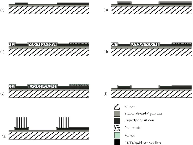
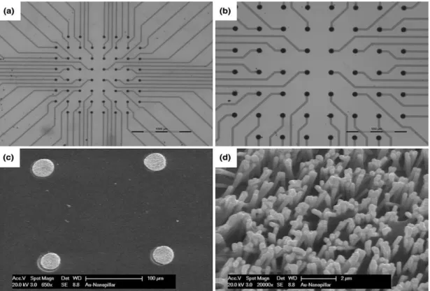
Figure 3.1. Main silicon-based MEAs micromachining steps: (a) Backside dicing, (b) Backside glassing and polishing, (c) Backside metallization, (d) Frontside dicing, (e) Frontside wet-etching………45 Figure 3.2. Schematic top-view of backside dicing including 9 collections of 5×5 matrix……...45
Figure 3.3. Isoetch contours and surface topography of etched silicon for the HF-HNO3-acetic acid diluents [33]. Numbers in parentheses shows etch rates of silicon in µm/min………...48 Figure 3.4. Experimental setup for dynamic etching process to round the side-walls of the square columns of the electrodes………...…………....49 Figure 3.5. Experimental setup for static etch process: (a,b) Photographs of the static etching process. In this step of etching, the tips are sharpened by applying the N2 gas from the bottom; (preferential etching)……….…..49 Figure 3.6. Process flow of electrodes tips-coating: (a) Parylene-C deposition, (b) Cover with dry-film photoresist, (c) Reactive Ion Etching, (d) Tip-metallization, (e) Lift-off in acetone….……..50 Figure 3.7. Structural phases during self-assembly of SWNT coffee stains: (a) SEM images of continuous, holey, striped, and spotty phases, (b) Schematic structural diagram as a function of SWNT and SDS concentrations. Reprinted with permission from Ref. [34]………57 Figure 3.8. A schematic of electrochemical measurement setup. Ag/AgCl act as a reference electrode, large area Pt wire as a counter, and electrodes of the array as a working electrode…...59 Figure 3.9. SEM images of electrodes backside: (a) Backside dicing, (b) Cross-section of the backside kerfs which have been filled with the glass paste, (c) 3D pyramid-shaped electrode array with three different heights. The outer row of electrodes is for etching process uniformity and will remove after etching step………..…………..…….59 Figure 3.10. SEM images of the electrode etching process: (a) Frontside cutting, (b) Rounding corners by stirring the etching solution, (c-e) Polishing and sharpening the tips of electrodes by applying N2 gas from the bottom of the solution, (f) One 3D 7×7 MEA……….60
Figure 3.11. SEM images of masking process: (a) Electrode array covered with dry-film
photoresist after RIE process. Dry-film photoresist follows the 3D structure of the electrodes, (b) Uniform tip-exposure of variable height electrodes after RIE and oxygen plasma etching process, (c) Electrode-tip after removing the mask………..…………..………..61
Figure 3.12. SEM images of microelectrodes after tip-metallization with Pt (a,b, c) and SIRO (d, e, f) at different magnification. The SIRO surface is rougher than Pt. SIRO has dendritic structure while Pt has granular morphology………..62
Figure 3.13. SEM images of microelectrodes after tip-coating with CNTs: (a-b) At different magnification. The geometry of CNTs increased the accessible surface area, (c) Pt particles at the end of CNTs………...63
Figure 3.14. SEM images of microelectrodes after tip-coating with CNTs using coffee stains technique: (a-d) At different magnification. Small white particles are SDS that were evaporated after heating the electrodes……….64
Figure 3.15. Impedance spectroscopy of Pt- and CNTs-coated electrodes: (a) Magnitude of impedance as a function of frequency, (b) Phase of the impedance as a function of frequency, (c) & (d) CV curves for CNTs- and Pt-coated electrodes of the MEA under similar condition, respectively……….66 Figure 3.16. Electrode tip dimensions; the height (h) and radius (r) of the tip…….………..67 Figure 3.17. Electrochemical measurement setup: Equivalent circuit of the electrode-electrolyte
interface………..69
Figure 3.18. Simulation and experimental results of equivalent electrode-electrolyte interface: (a) Pt-tips, (b) SIRO tip, (c) CNT-tip………...71
Figure 4.1. Schematic view of a silicon micromachined neural MEA with variable heights of 1.45, 1.55, and 1.65 mm. The shank was covered with parylene-C (or PEG) and the recording sites of each array were coated with Pt, Mo, Au, SIRO, or CNTs. The thickness of the electrodes was 200 μm at the base and less than 2 μm at the tip with 100 μm spacing………..……...78 Figure 4.2. A schematic view of hemocytometer as seen from the microscope. The cells marked as a circle in sections 1, 2, 3, and 4 was counted………...80 Figure 4.3. SEM images of microelectrodes: (a) Silicon-based microelectrode before coating with parylene-C and PEG, (b) Microelectrode coated with parylene-C, (c) Microelectrode covered with PDL, (d) Microelectrode covered with PEG……….……81 Figure 4.4. SEM images of the MEA surfaces coated with: (a) and (b) Pt, (c) and (d) Au, (e) and (f) SIRO before and after coating with the PDL, respectively………....……..82 Figure 4.5. FTIR spectrum of silicon MEA insulated with parylene-C and tip coated with PDL: (a) and (b) Mo coating before and after coating with the PDL, respectively. (c) and (d) Pt tip-coating before and after tip-coating with the PDL, respectively……….83 Figure 4.6. FTIR spectrum of silicon MEA insulated with parylene-C and tip coated with PDL: (a) and (b) Au tip-coating before and after coating with the PDL, respectively. (c) and (d) SIRO tip-coating before and after coating with the PDL, respectively. (e) and (f) CNTs tip-coating
before and after coating with the PDL, respectively. These measurements have been done using Perkin Elmer spectrum with a 65 FTIR spectrometer………...84 Figure 4.7. Optical microscopy of the electrode tips incubated with neuroblast cells: (a) Before coating with polymers, (b) Following coating with parylene-C, (c) Following coating with PEG hydrogel……….85 Figure 4.8. Total cell number before and after parylene-C and PEG deposition, (N=6)………..86 Figure 4.9. Optical microscopy of the MEAs incubated with neuroblast cells: (a) and (b) Pt, (c) and (d) Au, (e) and (f) SIRO, (g) and (h) Mo, (i) and (j) CNTs tips before and after PDL coating, respectively. Significantly more cells were attached to the PDL-coated electrodes than the uncoated ones (Table 4.2)………..88 Figure 4.10. Cell proliferation before and after PDL coating: (a) Total cell number of each coating before and after peptide deposition. (b) Cell proliferation per electrode site for each tip-coating before and after peptide deposition (N = 9). The cell proliferation has increased in the presence of the electrodes conjugated with PDL………...89 Figure 4.11. Growth curve for neuroblast cells via manual count using hemocytometer after 6, 12, 24, and 48 h. The lines present a mean value of four points obtained in three separate experiments. Standard deviations have been indicated………...……….……..90
LIST OF ABBREVIATIONS
CNS Central Nervous System
BMI Brain-Machine Interface
MEA Microelectrode Array
CNTs Carbon Nanotubes
PECVD Plasma Enhanced Chemical Vapor Deposition
PEG Polyethylene Glycol
PDL Poly-D-Lysine
FTIR Fourier Transform Infrared
SEM Scanning Electron Microscopy
ETC Electrode-Tissue Contact
EIS Electrochemical Impedance Spectroscopy
CV Cyclic Voltammetry
SIRO Sputtered Iridium Oxide
MEMS Micro-Electro-Mechanical Systems
SNR Signal-to-Noise Ratio
Ppy Polypyrrole
PEDOT Poly (3, or 4- ethylenedioxythiophene)
CMOS Complementary Metal–Oxide–Semiconductor
HRTEM High-resolution transmission electron microscopy
DRIE Deep Reactive Ion Etching
SOI Silicon-On-Insulator
PDMS Polydimethylsiloxane
EDM Electrical Discharge Machining
CPE Constant Phase Element
CoV Covalent
MWCNTs Multi-Walled Carbon Nanotubes
PSS Polystyrene Sulfonate
TDT Tucker Davis Technologies
HF Hydrofluoric acid
pMEA Planar Microelectrode Array
CVD Chemical Vapor Deposition
RIE Reactive-Ion Etching
SWNTs Single-Wall Carbon Nanotubes
SDS Sodium-Dodecyl-Sulfate
EDX Energy-Dispersive X-ray
LSA Lateral Surface Area
EMEM Eagle's Minimal Essential Medium
FBS Fetal Bovine Serum
ROS Reactive Oxygen Species
H2O2 Hydrogen Peroxide
OH· Hydroxyl Radical
HO2· Hydroperoxyl Radical
O2- Superoxide Onion
PEG-PL Polyethylene Glycol-Lipid
HFCVD Hot Filament Chemical Vapor Deposition LPCVD Low Pressure Chemical Vapor Deposition
CHAPTER 1 INTRODUCTION 1.1 Scope of the thesis
Neural microelectrode arrays (MEAs), which act as an interface between neural tissues and bioelectronic devices, play an important role in chronic implants and must be reliable, stable, and efficient for long-term recording and stimulation. Electrochemical properties and biological compatibility of chronic microelectrodes are essential factors that must be taken into account in their design and fabrication. This thesis brings aspects of these two factors together, exploiting the unique properties of new MEA to address challenges currently faced by neural implants. In this thesis, a new 3D micromachining technique along with organic coatings is proposed for the fabrication of high performance MEAs. All the process steps starting from substrate preparation, to coating procedures using metallic thin-films and organic materials, along with electrochemical characterization and biocompatibility tests are presented in details. The role of geometry and materials on MEAs performance is particularly discussed and clarified.
In this chapter, we first summarize the current performance, limitations, and challenges of implantable microelectrodes. We then highlight the specification of new fabricated MEAs and explain how these can improve microelectrodes performance.
1.2 The advent of penetrating Microelectrode arrays (MEA)
Intracortical implants as a part of neuroprosthetic devices are in direct contact with the cerebral cortex of the brain. During the past four decades, the concept of interfacing with the brain cortex for both recording and stimulation the nervous system has rapidly evolved [35, 36]. Intracortical prosthesis that penetrates into the brain can stimulate an immediate area of the brain by directly interfacing the cortex depending on their design and placement [37, 38]. Besides, required electrical currents to stimulate neurons through penetrating electrodes are much smaller than those used to excite neurons through surface stimulation.
Penetrating MEAs have been developed for vision, auditory, and cognitive implants. Visual implants can partially restore vision by directly stimulating the visual cortex and is still the only hope of providing vision for patients with pathologies when the optic nerve is disconnected from
retina to the vision center of the brain. The first attempt to restore vision through cortical stimulation began in 1970 with Brindley and Dobelle [39-41]. Dobelle’s 64 channel surface electrode array was placed on the top of visual cortex which allowed blind patients to recognize shapes in slightly close distances. The challenges were a lack of control of the number of phosphenes, pain induced by the large current stimulation of large electrodes, and more importantly no access to inner neurons that is necessary to stimulate. Intracortical stimulation was introduced to overcome those problems. Penetrating MEAs provide high fidelity images with a lower energy leading to less damage to neural tissues. Moreover, these MEAs could produce a more localized stimulus with less current. Schmidt et al. [42] showed that phosphenes could be evoked with lower currents than surface stimulation current and simple patterned perceptions could be evoked by small groups of penetrating MEAs. Penetrating microelectrodes provide capability for simultaneous cortical and thalamic recording from auditory cortex [43]. They have also shown great promise for restoring neurological lost functions, stroke, or injury [23]. However, considerable obstacles have to be overcome for these cortical implants go from the lab-bench on to the commercial reality.
1.3 Current challenges
Perhaps the most significant obstacles to the MEAs technologies are low impedance pathway for higher charge transfer, high-spatial resolution, and biological compatibility of the microelectrodes. For electrical stimulation and recording, electrodes with multi-dimensional geometry, high selectivity and sensitivity are needed. The selectivity is defined as an ability to activate individual neurons without activating identical neighbors. In order to obtain high selectivity, electrodes must be in close contact with tissues and this can be achieved using a 3D high-density MEA with small surface area of active sites [44, 45]. 3D penetrating MEA where the active sites of the electrodes are not in a same plane offers the best spatial selectivity. However, when the area of electrode decreases, the electrode impedance increases, which affects the stimulating/ recording characteristics (sensitivity) [46]. Electrode performance is a compromise between high selectivity that can be obtained by using smaller electrodes and the resulting increase in impedance and lower sensitivity. An approach to lower the impedance of the electrodes is modifying the interface material, for example by using organic nanomaterials with large surface area [47, 48].
Another significant limitation of the MEAs technologies is biocompatibility of the electrodes which is an important issue that must also be addressed. For clinical applications, MEAs must be reliable, stable, and efficient for long-term recording and stimulation [49]. When the MEA are inserted into brain tissue, numerous foreign body responses can occur, often resulting in a lack of biocompatibility of the implants. For example, if the electrodes are implanted for long periods of time, the formation of glial scar tissue can occur, which can encapsulate and isolate the electrodes from the neurons, resulting in a loss of electrical connectivity and increased impedance [50]. To avoid this problem, it is important to improve the biocompatibility of the electrodes. One of the strategies that can be used to minimize immune response to implanted electrodes is by coating them with bioactive molecules such as cell adhesion peptides or proteins. These peptides not only improve cell adhesion but also increase the cell proliferation [51]. Brain implant surgical operations are extremely high-risk for patients, so electrodes safety and efficiency must be well examined and verified before implant. Neuroprostethic devices are susceptible to the tissue response that causes failure in implanted electrodes. Therefore, the impact of implant presence in vivo over extended periods of time must be monitored.
Despite all the limitations and challenges, intracortical implants are the only way that have shown promise for restoring neurological functions lost to patients who have, for example in vision domain, a complex damaged retina, optic nerve, or lateral geniculate body [37].
It is widely understood that the challenges faced by the MEAs technology is largely finding appropriate geometry and materials that enhance consistent long-term recording/stimulation of large neuronal populations and improve electrodes biocompatibility. In recent years, nanotechnology has increased enormously to provide novel fabrication methods and materials. Conducting polymers and carbon nanotubes (CNTs) have attracted much interest as suitable materials for coating the electrodes. CNTs possess the exceptional chemical stability, electrical transport and mechanical properties to ameliorate both recording and electrical stimulation from/of neurons [17]. Strength and stiffness of CNTs prevents the tips of the electrodes from being fractured. The molecular/cellular biology approach attempts to minimize the immune response to implanted electrodes by using bioactive molecules. Such an approach is focused on
coating electrodes with peptides or proteins [51]. Still the implant microelectrodes technology needs to truly improve the technology to the level of clinical implementation.
1.4 Microelectrode arrays: a key element in neuroprosthetic devices
The major goal of the emerging field of neurotechnology is restoration of nervous system disorders. Neuroprosthetic devices that can record neural activities and stimulate the central nervous system (CNS), called brain-machine interfaces (BMI), enable direct communication with still-functioning parts of the neural pathways and offer significant potential to restore various lost neurologic functions of patients with vision impairment, epilepsy, Parkinson's or depression [52]. A key element in functions restoration is MEA dedicated to interface neural tissues [53]. The ultimate role of the MEA is to provide precise measurement and provide safe electrical stimulation of neural activities when chronically implanted in the cortex.
Remarkable progress has been reported at most bioelectronic levels of implantable BMI, but the electrode-tissue contacts (ETCs) remain one of the major obstacles. Contacts achieved using MEAs do not comply with the remaining parts of these BMIs due to the biological response to chronic implantation and to the electronic properties of MEAs. The success of these BMIs relies on electrodes which are in contact with the neural tissue. However, design and fabrication of an ideal interface with selectivity, good electric characteristics, sensitivity, biocompatibility, and long-term chemical and recording stability remain a tough challenge.
To date, implantable MEAs have been fabricated by three common techniques: microwire, micro-machined, and flexible arrays [1]. Microwires (made from tungsten or stainless steel) are used to focus on the individual neuron [54].One particular advantage of microwires is that they can be applied to access deep brain structures but the accurate location of the electrode tips relative to each other is not controllable because of the wire bending during implantation. Micro-machined electrode arrays can be silicon- or metal-based. This technique provides a higher density of electrode-tissue interface which reduces tissue displacement compared to microwires and contains active electronics integrated into the arrays [3, 25, 55]. These electrodes are designed to be implanted in the cerebral cortex or peripheral nerves. Flexible multi-electrode array is another type of electrode that provide an advantage over the rigid electrode arrays because of the closer mechanical match with brain tissue; however, the flexible nature of these electrodes involves some difficulties during insertion [56].
In recent years, MEAs techniques have been developed to have a long-term and stable interface with the tissues with the brain. Several research groups try to obtain consistent recording signals from small groups of neurons without losing microstimulation capabilities while maintaining low-impedance pathways for higher charge injection and high-spatial resolution by altering the material compositions and geometries of the arrays [57]. So far, none of these attempts have lead to a major breakthrough.
Our goal this thesis is to elaborate a biocompatible 3D MEA with high selectivity and sensitivity, good electrical conductivity, and high density of microelectrodes.
1.5 Objectives of the present work
The objectives we set out to accomplish at the beginning of this doctoral thesis project was design and fabrication of 3D, high-density, penetrating MEA for intracortical neural recording and stimulation. In particular, we wanted to improve the effectiveness of MEAs by a 3D structure when the needles have variable lengths such that the tips are no longer in the same plane, increase the density of the electrodes, decrease the impedance, and increase charge transfer. We also wanted to improve biocompatibility and durability of the electrodes for long term operation of the device implanted in neural tissue. The MEAs should cause minimum tissue response, i.e. encapsulation and inflammation. In addition, the ease of fabrication was important because when arrays become 3D, smaller, and higher in density, fabrication techniques are challenged to meet the dimensional and processing tolerances.
The thesis project can be summarized by the following objectives:
Implement a novel micromachining technique to fabricate variable-height, penetrating, high-density neural MEAs that enable intracortical 3D recording and stimulation from/ of neural tissues
Novel dry-film based masking technology that enhances uniform tip-exposure for electrodes with variable-heights and improve the conventional process which is costly and time-consuming
Optimize the electrical properties of electrodes in order to achieve both the low impedance and high charge transfer by selective direct growth of CNTs on the tips of 3D MEAs
Study the electrochemical behavior of MEAs as a function of frequency; electrochemical impedance spectroscopy (EIS), cyclic voltammetry (CV), and electrodes modeling
Evaluate the impact of parylene-C, polyethylene glycol (PEG) hydrogel, and poly-D-lysine (PDL) on the biocompatibility of the MEAs while ensuring compatibility of the microelectrodes with neuroblast cells; cell culture and in vitro tests
1.6 Specifications of projected MEAs
The 3D MEAs, shown in Figure 1.1, provide a multichannel interfaces to the cerebral cortex. Micromachined electrode array is a 5×5 matrix of 1.65, 1.55, and 1.45 mm long electrodes in two perpendicular directions in order to create a pyramid-shaped array. The thickness of the electrodes is 200 μm at the base and about 2 μm at the tip with 100 μm spacing. Electrodes project out form a single block of a thin (2150±25 µm) p-type silicon (100) with a resistivity of 0.0153-0.0158 Ωcm while electrically isolated one from each other with glass paste from the backside. To make electrical connection to each electrode, the backside of each pin is metalized. The entire upper surface of the MEA (i.e. excluding the tips) is insulated with parylene-C. The tips of the electrodes are sputter-coated with Pt and iridium oxide using a novel masking method that enhances uniform tip-exposure for variable-heights electrodes. The tips of other group of arrays are coated by selective direct growth of CNTs while the shanks are insulated with native SiO2. The variable-height penetrating MEAs presents a large surface area to the cortex and has the strong advantage that it floats in the cortical tissues. As the cortex moves the array moves with it, as a result producing little or no relative motion between the active sites and the neurons around it.
In order to improve biocompatibility of the MEAs, the surface of the electrodes is coated with PEG hydrogel which is a biocompatible polymer. To improve neural-cell adhesion and proliferation and also prevent electrodes encapsulation when they are implanted in vivo, electrodes are coated with bioactive molecules (PDL). The novel architecture of this MEA makes it unique among the currently available micromachined electrode arrays, as it provides higher density contacts between the electrodes and targeted neural tissue facilitating stimulation or recording from different depths of the brain.
Figure 1.1. Schematic view of a silicon micromachined neural MEA with variable heights of 1.45, 1.55, and 1.65 mm. The shank was covered with parylene-C (and PEG) and the active sites of each array were coated with Pt, sputtered iridium oxide (SIRO), or CNTs. The thickness of the electrodes was 200 μm at the base and about 2 μm at the tip with 100 μm spacing.
1.7 Summary of contributions
In this thesis, we have achieved 4 main contributions with respect to the improvement of the neural MEAs performance implanted in neural tissues.
Implement a novel pyramid-shaped, high-density, penetrating MEA: a micromachining technique was developed for building penetrating 3D MEA with a high electrode-density when the tips are no longer in the same plane in 2 perpendicular directions. The issue with current available array is that it is 2D and provides recording data from a plane of the brain. Even the slanted one is quasi-3D instead of 3D [23]. Such 3D high electrode-density array (25 electrodes/1.96 mm2) is expected to record from different depths of the brain and provide more contacts between the electrodes and targeted neural tissue (greater access to neurons). The importance of such pyramid-shaped MEA has not been quantified but may have significance during injection electrodes inside the tissue. Variable-height electrodes may help to investigate more about neurons causal interactions (“effective connectivity”).
Introduce a novel masking technology: to coat the 3D pyramid-shaped MEA, a novel masking method was developed that resulted uniform tip-exposure for variable-height
electrodes and improved process time and cost significantly. The new method needs single masking step and reduced the conventional masking process steps from 14 to 6.
The new procedure has several advantages including simpler and easier fabrication process, reduced production time and cost, and more uniform tip-exposure. More importantly, the conventional masking methods may not be practical for 3D MEAs since they cannot follow 3D structures.
Optimize the electrical properties of MEAs: the impedance is one of the most important electrical properties for microelectrodes. In order to achieve both the low impedance and high charge transfer, the electrodes were coated with CNTs by selective direct growth on the tips of 3D MEAs for the first time using Plasma Enhanced Chemical Vapor Deposition (PECVD). The CNTs coating led to a 5-fold decrease in impedance and a 600-fold increase in charge transfer compared with Pt electrode.
Improve biocompatibility of the MEAs: electrodes were coated with PEG hydrogel (well-known biocompatible polymer) to improve biological compatibility of the electrodes. In the next step, electrodes were coated with bioactive molecule; PDL. An in vitro study was performed to test the capacity of PDL to improve neural-cell adhesion and proliferation. Increased proliferation of the neuroblast cells on the microelectrodes was observed in the presence of the PDL. The PDL coating increased cell adhesion by more than 50%. It is noteworthy that the arrays with CNT active sites had greater cell numbers than the electrodes with metallic tips, both before and after PDL deposition. These results show that the CNTs increased biocompatibility and enhanced cellular responsiveness by attracting more neural cells.
1.8 Organization of the thesis
This thesis is presented in 5 chapters. In chapter 2, we review and compare different MEAs technologies and their characteristics. A technical overview of recent advances in the field of microelectrodes fabrication, characterization, and modeling is given. Moreover, the effect of different coatings to improve electrical properties and biocompatibility of the electrodes is presented.
The main body of the thesis is presented in chapter 3 and 4. In chapter 3, the experimental procedures of MEAs fabrication are described in detail. This chapter provides in depth explanation to the experimental techniques and characterization tools that were used during the course of this work. Next, the experimental results of MEAs microfabrication process, novel masking technology, direct growth of CNTs at the tips of the 3D MEAs, and the influence of CNTs on the electrical properties of the electrodes are presented. Besides, electrical circuit model of microelectrodes is presented in this chapter. In chapter 4, two different techniques to improve MEAs biocompatibility are presented. The role of biocompatible polymers and bioactive molecules to promote and stabilize cell attachment on the surface of the microelectrodes will evaluate by in vitro cell-culture tests.
Finally, Chapter 5 provides a general discussion of the results that are presented in the thesis. We will discuss what implications our work will have in the future of intracortical MEAs. The document will end with general conclusions and possible future work on fabricated MEA.
1.9 Publications
This thesis research has generated several results which were published in the form of scientific journal articles, poster, and oral presentations.
PUBLICATIONS:
B. Ghane-Motlagh, M. Choueib, A. H. Mesgar, Md Hasanuzzaman, and M. Sawan, “Direct growth of carbon nanotubes on new high-density 3D pyramid-shaped Microelectrode Arrays for Brain-Machine Interfaces,” Submitted to the Journal of Biomedical Microdevices.
B. Ghane-Motlagh, T. Javanbakht, F. Shoghi, K. J. Wilkinson, R. Martel, and M. Sawan, “Physicochemical properties of peptide-conjugated microelectrode arrays and their in vitro effects on Neuroblast cells,” Submitted to the Journal of Materials Science and Engineering. B. Ghane-Motlagh, Mohamad Sawan, “High-Density Implantable Microelectrode Arrays for
Brain-Machine Interface Applications, “ Advances in Science and Technology, 2014, 96, 95-101 .
B. Ghane-Motlagh, M. Sawan, “Design and Implementation Challenges of Microelectrode Arrays: A Review,” Materials Sciences and Applications, 2013, 4, 483-495.
POSTER AND PRESENTATIONS:
B. Ghane-Motlagh, T. Javanbakht, F. Shoghi, K. J. Wilkinson, R. Martel, and M. Sawan, “High-Density 3D Microelectrode Arrays for Brain-Machine Interfaces,” 37th Annual International Conference of the IEEE Engineering in Medicine and Biology Society (EMBC15), Milan, Italy, 2015.
B. Ghane-Motlagh, M. Sawan, “High-Density 3D Pyramid-Shaped Microelectrode Arrays for Brain-Machine Interface Applications,” 10th BioCAS Conference of the IEEE, Lausanne, Switzerland, October 2014.
B. Ghane-Motlagh, M. Sawan, “High-Density 3D Silicon-Based Microelectrode Arrays for Brain-Machine Interface Applications,” 36th Annual International Conference of the IEEE Engineering in Medicine and Biology Society (EMBC14), Chicago, USA, 2014.
B. Ghane-Motlagh, M. Sawan, “A Review of Microelectrode Array Technologies: Design and Implementation Challenges,” Second International Conference on Advances in Biomedical Engineering (ICABME13), Tripoli, Lebanon, 2013.
B. Ghane-Motlagh, M. Sawan, “High-Density Microelctrode arrays,” 6th International Research Network on Nano and Micro Systems (NAMIS) Autumn School, Tokyo, Japan, 2012.
CHAPTER 2 OVERVIEW OF IMPLANTABLE MICROELECTRODE ARRAYS This chapter will be devoted to a review of the microelectrode arrays (MEAs) which are using for stimulation and recording of/ from neural tissue. Both stimulation and recording microelectrodes use the same type of fabrication technologies. Next, the electrical and mechanical properties of the MEAs will be presented. Moreover, MEAs applications and variety of technologies that have been used to fabricate MEAs will be described and discussed. In addition, different methods to improve biocompatibility of the electrodes will be reviewed. Finally, an overview of recent advances in the field of implantable MEAs, equivalent circuit model, and perspective of this work will be given.
2.1 Introduction to neural MEAs
Neural MEAs are spatial arrangement of microelectrodes which serve as the first critical interface to the neural tissue for either signal recording or for tissue stimulation. Neural microelectrodes can be either penetrating or surface electrodes. The penetrating MEAs can measure small signals and require less power to stimulate neurons due to their high selectivity and sensitivity. Therefore, they are preferred for stimulate single units and fast recordings. The surface electrodes have low selectivity and sensitivity; however, they cause less tissue damage because they do not penetrate in neural tissue. In this thesis, our scope is penetrating MEAs. The first type of microelectrodes in neural investigations were metal wire electrodes to monitor the extracellular electrical activity in 1950s [31]. The rapid development in microfabrication technology accelerated the advent of silicon-based MEAs. In 1970s, Wise et al. reported the first micromachined silicon-based MEAs to interface neural tissues [58]. Since this pioneer work, silicon-based microfabrication techniques are among the dominant tools in fabrication of neural microelectrodes. Silicon MEMS (micro-electro-mechanical systems) technology including micromachining techniques, photolithography, and thin-film deposition provided well-defined size and spacing of recording sites, high accuracy, the repeatability, and low cost fabrication scheme [59]. Besides, silicon micromachining facilitate the direct integration of electronic circuitry on the backend of active microelectrodes [60-62]. Silicon-based MEAs have been shown promising results in terms of biocompatibility for chronic implant in vivo; however, to improve the signal quality and long-term reliability the issues including implantation method,
physical and chemical properties of coating materials have to be considered [63-66]. The progress in microfabrication techniques enhanced the combination of functional silicon and polymer parts to reduce the mechanical mismatch between the neural tissue and the implant [67, 68]. Furthermore, 3D structure of the arrays has shown the potential for high-density recording and stimulation [69]. All the above results present the versatility of silicon MEAs technology for specific neural applications. The recent breakthroughs can conclude that there is still a lot of room to combine the state-of-the-art technology with that of silicon microtechnology for new possibilities to increase the resolution of stimulation and recording techniques [70].
Different types of MEAs are functionally similar in terms of recording or stimulation requirements, but the devices are different in depth including spatial arrangements and size of active sites, fabrication techniques, materials, and extensibility of advanced and organic materials. Critical parameters which affect the performance and effectiveness of the MEAs are:
The density of the electrodes which is the ability of an array for higher or lower spatial resolution during recording and stimulation.
The architecture of the MEAs as it can enhance the access to different depth of the brain and also to individual neurons.
The impedance of the electrodes that should be low to reduce the stimulation voltage and the power. The high electrode impedance limits the ability to resolve the relatively weak neural signals.
The mechanical compatibility of the electrodes (coating electrodes with polymers) with neural tissue that may minimize trauma to tissue during insertion.
The durability and reliability of the MEAs is important for long-term operation of the electrodes.
The biocompatibility of the electrodes must be taken into account to minimize the tissue response.
Ease of fabrication should be considered as MEAs become smaller and challenges will be increased.
2.2 Properties of MEAs
The mechanical, electrical, and biological properties affecting the performance of the MEAs are discussed and reviewed in this section.
Mechanical properties: the shape, architecture, and materials are some of the important factors that can affect the mechanical properties of the electrodes [71]. The MEAs should be architecturally compatible with the geometry of the targeted tissue. A fit match between the array and the neural tissue avoid gap between them resulting less fibrotic tissue developed between the array and the target area. The 3D structure of the array with high electrode density may excite more population of neurons. Furthermore, the array geometry plays an important role in the tissue damage during the insertion e.g. design very sharp electrodes can help to reduce tissue damage. The brain tissue to compare with the electrode materials is relatively soft. The Young’s module of the brain is between 15.9 Pa and 42.6 Pa [72]. To reduce reactive response, we have to choose the materials with Young’s modulus close to the brain tissue.
Electrical properties: one of the most important electrical properties of the electrodes is impedance which is characterized as the magnitude of the impedance at 1 kHz; frequency that is used for neural electrodes since the center of energy of action potentials is about 1 kHz [73]. The impedance of the electrodes depends on the surface area (R = ρl/S) of the active site (tip exposure). To reduce tissue damage and increase the selectivity, smaller electrodes are desired and the result will be high impedance and less sensitivity. Using materials with intrinsically larger surface area not only decreases the impedance but also increases the charge transfer through electrodes to the targeted tissue. In order to have identical electrical properties of each electrode in an array and interpret recorded signals during physiological experiments reliably, tip exposures should be uniform.
Biocompatibility: the implanted MEAs should not damage cells, tissue or enzymes, should not evoke a toxic, and should be stable in a long term without encapsulation. The most dominant reasons for short-term immune response are geometry (shape and size) [29], mechanical impact (design and implantation parameters) [74, 75], and surface properties [76]. Aforementioned parameters can efficiently contribute to delay or control immune response of the surrounding tissue in chronic implants. When the MEA are inserted into brain tissue, numerous foreign body
responses can occur. For example, if the electrodes are implanted for long periods of time, the formation of glial scar tissue can occur, which can encapsulate and isolate the electrodes from the neurons, resulting in a loss of electrical connectivity and increased impedance [50].
2.3 Application of penetrating MEAs
Neural interfaces, which allow direct and selective stimulation and recording of/ from neural tissues, offer significant potential to understand neurophysiological processes of human functions and behavior. They have also represented great promise restoring various neurological functions lost to disease, stroke or injury, control of assistive instrumentation for the patient with motor dysfunction, and neural prostheses to restore vision and auditory perception. In patients with neurological disorders, the communication between central or peripheral nervous system is damaged or disconnected that can cause full or partial paralysis of motor or sensory skills. The field of neuroprosthetic devices has been focused for many decades to improve the quality of life of paralyzed patients [77-80]. A part of goal of developing neural interfaces is to record neural signals. The firing pattern of neural signals, coming from the motor cortex, during a certain operation are recorded by implanted high-density MEAs then decoded and combined with behavioral changes to correlate the signals with certain “movement interactions”. Thereby, a neural interface can potentially allow a patient to control her prosthetic limbs using intuitive movement intentions.
The design of neural interface devices depends on the application. Neural interface devices have been developed for application in the brain cortex, eye, ear, or around peripheral nerves [39, 81]. Over the past few years, an increasing number of studies have focused on MEAs that will interface to neurons of the visual cortex [12, 42] or to neurons of the retina [37, 82]. Neural interface devices are implanted chronically onto the visual cortex of a blind patient to electrical stimulation to restore the vision. Cochlear implant is the most successful biomimetic device which is already in commercial use [83]. The relative complexity of visual system and intracortical implant presents challenges to researchers attempting visual prostheses.
Develop a chronically stable interface for exchange of information between implanted device and biological environment is essential for any neural prosthesis. The current neural interface
application is based on using metal-, silicon-, or polymer-based microelectrodes placed in proximity of the target neurons (Figure 2.1).
Figure 2.1. Implanted microelectrode in the cortex. Neural stimulation occurs via current passes through the tip to the surrounding neurons. Reprinted with permission from Ref. [13].
2.4 Fabrication technologies of penetrating MEAs
To this date, penetrating MEAs have been fabricated by a number of different techniques: microwires, micromachining, and flexible electrode approach. Since the fabrication technique affects the functionality of the microelectrodes some essentials should be taken into account in their design and fabrication such as 1) ease of fabrication to allow mass production, 2) ability to develop high-density sharp electrodes with various 3D architecture suitable for insertion into the cortex, and 3) compatible with IC manufacturing techniques. In terms of substrate material for the MEAs, silicon is still preferred material for fabrication and has been shown promising results; especially its chronic in vivo performance is quite remarkable also it can be shaped with
precision greater than perhaps any other material. Moreover, integrated electronic connect directly to the MEAs with using different packaging techniques.
In this section, we will review and discuss aforementioned techniques and their advantages and drawbacks.
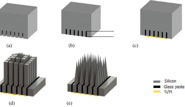
2.4.1 Traditional Microelectrode arrays Metal-wire electrodes
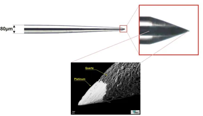
One of the traditional neural probes is single metal-wire electrode consist of a metal needle covered by insulation except at the tip. The tip of the wire is etched to form a sharp needle-shaped electrode. The entire surface of the metal-wire (excluding the tips) is insulated with quarts glass, Teflon (trafluoroethylene- TFE), or polymer films such as parylene and polyimide. Different types of metals like stainless steel, tungsten, platinum, iridium, and titanium nitride are used as a wire (Figure 2.2). Although the metal-wire electrode has a very sharp tip it is difficult to control the position and size of the opening of the electrodes.
Figure 2.2. Scanning electron microscopy (SEM) images of Glass insulation and the metal part
Glass electrodes
Another type of neural electrodes are micropipettes that penetrate to the cell membrane and are generally used for intracellular studies. The common technique in the fabrication of such micropipette electrodes involves a two-stage pulling process. Briefly, a thin walled glass capillary tube which is 1 to 2 mm in diameter is heated electrically along the two extremities. When some extension occurs at the softened glass then larger tension is applied to make sharp tips at the breaking point. The diameter of the tip and the shank can be controlled by changing the pulling force and the temperature. To form the conductive path to the tissue, the micropipette is filled with an electrolyte like KCl. Such micropipettes have a very thin cone at the tips which is very fragile and hard to fill with electrolyte. They have also very high electrical resistivity. These types of neural probes are limited by high impedance and making an array of electrodes [84]. Figure 2.3 shows scanning electron microscopy (SEM) images of pre-processed pipettes (top) and optical microscopy images of conventionally processed pipettes.
Figure 2.3. SEM (top) and Optical microscopy images of pre-processed and conventionally processed glass pipettes. Reprinted with permission from Ref. [15].
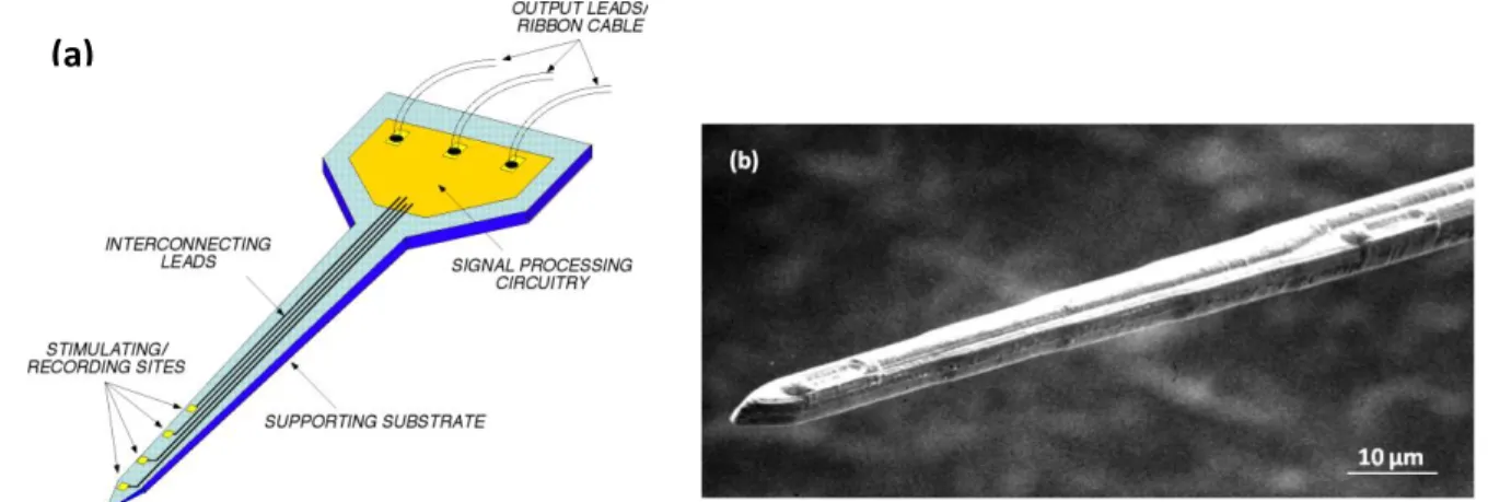
2.4.2 Microwires
Microwires, made from tungsten or stainless steel, were the first implantable electrode arrays to record chronically from the brain. Their narrow structures let them be placed very close to single neurons in vivo. One advantage of microwires is that they can be applied to access deep brain structures [54]. Microwires typically consist of metal needles insulated with polymer film (parylene or polyimide) except at the tips. The tips of the metal wires are electrochemically etched to form a sharp tip. The diameter of the wires is normally less than 100 µm. Electrodes are then micro-welded and glued to a laser-drilled ceramic substrate to make a multiple-electrode array (Figure 2.4) [85, 86].
Figure 2.4. Microwires: (a) Wire microelectrodes embedded in ceramic substrate. The anchors ensure that the array stay in the brain, (b) Ceramic well-structure connected to parylene-C insulated gold wires. Electrodes are inserted perpendicular into the substrate, (c) SEM image of microwire insulated with 3 µm parylene-C except at the tip. Reprinted with permission from Ref. [16].
Metal microelectrodes are fabricated from different types of materials such as stainless steel, tungsten, platinum, iridium, or gold. Since stainless steel is fragile near the tips, tungsten was replaced due to the stiffness and rugged structure, and to provide very stable recordings;
however, tungsten is very noisy at low frequencies [87]. A platinum electrode plated with platinum black gives stable recordings, high signal-to-noise ratio (SNR), and creates a porous low-impedance structure, but it is mechanically fragile [88]. Iridium metal wire is extremely stiff, highly resistance to corrosion, and its surface is electrochemically activated, which causes it to increase the maximum charge density [89]. Microwires remain in use today and fabrication methods have not changed basically. They give long-lasting individual neurons recording, sometimes more than one year, so they allow neuroscientists to focus on individual neurons [86]. In all the above-cited cases, the final contact between electrodes and brain tissue is a metal.
Recently, carbon nanotubes (CNTs) have been used to coat the tips of the metal wire electrodes. In 2008, a group of researchers in Texas coated the tips of conventional tungsten and stainless steel wire electrodes with CNTs using electrochemical deposition method (Figure 2.5). CNT-coated electrodes not only provided an appropriate substrate for neural growth but also improved both the recording and stimulating characteristics of neural electrodes [17].
Figure 2.5. SEM images of metal microelectrodes coated with CNTs: (a) CNTs covalently attached to the tungsten electrode, (b) CNTs were electrochemically deposited at the recording sites of the electrode. Reprinted with permission from Ref. [17].
One particular disadvantage of microwires is bending of the wires during implantation, so the accurate location of the electrode tips relative to each other is not controllable. The micro wire electrode arrays are also limited in their geometry and reproducibility, causing considerable insertion tissue damage, and they are not always compatible with silicon-based integrated circuits.
(b) (a)