HAL Id: hal-00878264
https://hal.archives-ouvertes.fr/hal-00878264
Submitted on 29 Oct 2013
HAL is a multi-disciplinary open access
archive for the deposit and dissemination of
sci-entific research documents, whether they are
pub-lished or not. The documents may come from
teaching and research institutions in France or
abroad, or from public or private research centers.
L’archive ouverte pluridisciplinaire HAL, est
destinée au dépôt et à la diffusion de documents
scientifiques de niveau recherche, publiés ou non,
émanant des établissements d’enseignement et de
recherche français ou étrangers, des laboratoires
publics ou privés.
An asperity-based finite element model for electrical
contact of microswitches
Hong Liu, Dimitri Leray, Patrick Pons, Stéphane Colin
To cite this version:
Hong Liu, Dimitri Leray, Patrick Pons, Stéphane Colin. An asperity-based finite element model for
electrical contact of microswitches. IEEE Holm Conference on electrical contact, Sep 2013, Newport,
United States. pp.PID1143448. �hal-00878264�
An asperity-based finite element model for electrical
contact of microswitches
Hong Liu
1,2Dimitri Leray
1,2Patrick Pons
2Stéphane Colin
11Institut Clément Ader, INSA Toulouse 2CNRS, LAAS; Univ Toulouse, INSA, LAAS
Toulouse, France
Abstract—Precise prediction of electrical contact resistance is important for microswitches. The contact spot used to be considered as a circle in earlier literature, where there was only one geometrical parameter: the radius of the a-spots. However, a real contact asperity has a height and an angle with the interface. In this paper, a 3-dimensional cone-truncated geometry is used to model an asperity, and three parameters are defined: radius, height and the angle of the side with respect to the surface plane. The ranges of their values are extracted from AFM measurement of samples in Au and Ru, and the values match well with the previous mechanical simulation results.
Compared to the theoretical results, the finite element (FE) model showed a good capability to predict contact resistance in the diffusive regime, but underestimated it in the ballistic regime. The effects of angle and height of the asperity were investigated for Au-Ru contact in terms of contact resistance, maximum temperature and its location. Regarding multiple spots in contact, this work investigated the influence of the number of spots and their distributions for contact resistance and local Joule heating.
Keywords— microswitch, asperity-based, finite element model, electrical contact resistance
I. INTRODUCTION AND MOTIVATION
As is well known, contact resistance is of significant importance for the performance of ohmic microswitches, and should be predicted accurately. For microswitches, as they are usually activated under very weak force, of about tens or hundreds of micro-Newtons [1-3], contact is made only at the highest asperities. Typical dimensions of asperities, often called a-spots, range from tens to hundreds of nanometers [4-6]. Contact resistance, in the case of one spot, can be calculated analytically according to the ratio between the contact radius and the mean free path of electrons. Three electron transport regimes can be defined [7]: diffusive, ballistic and quasi-ballistic, and the formulae were provided correspondingly [8-11].
However, all of the formulae supposed that contact occurs between two infinite surfaces, and only the contact radius was
taken into account as the geometrical parameter of contact. Regarding the form of a contact asperity, Holm [8] modified the expression for an elliptical spot, and Nakamura [12] applied a boundary element method to calculate the contact resistance of a spot in the form of a square and a ring. The contact spot was discussed in 2-dimension here.
Furthermore, Sano [13, 14] investigated the effect of the space angle on the constriction resistance. The space angle was defined as the angle made by the asymptote surface with the extension of the contact surface (see Fig. 1). The constriction resistance depending on the space angle 1 was then evaluated with: 4 tanπ+α = cH c R R (1)
where RcH is the constriction resistance calculated with Holm
formula (RcH=2/2a).
His results showed that the space angle had a quite important effect on the constriction resistance. However, the space angle was neglected by most of the researchers, except for Rezvanian et al. [15], who built an asperity model in conical geometry and showed that the space angle played an important role on the creep mechanism.
Fig. 1. Asperity model suggested by Sano [13]
Considering rough surfaces of the contact bump and the drain electrode in microswitches, an asperity in contact should have a height, and the side of asperity then has an angle with
respect to the surface plane. Motivated by this, a 3-dimensional (3D) model is proposed in this paper.
The current is constricted when passing through small asperities, heating in contact is extremely localized on the asperity proximity [16]. Another concern in the work is to investigate the thermoelectrical behavior of electrical contacts. An analytical expression for voltage-temperature (V-T) relation was given by Holm [8], in which the maximum temperature depended only on the total voltage of a long constriction; while for the small spots, size on the order of mean free path, the expression of Holm was invalid [4]. Jensen et al. then considered the ballistic effect, and introduced an improved model for small spots [16].
Also the numerical coupled-simulations have been proved to be an efficient method to study the thermoelectrical behavior of contact, and have been adopted by many researchers [17-22]. Among them, the research of Leidner et al. [21,22] seems more pertinent, in which the current density distribution for contact with layered structure and ‘real world’ contact topographies were discussed, and the simulation results were confirmed with the thermal images by infrared thermography [22]. However, the study was for the connector system, in which the contacting spots were much larger than in the case of microswitches, and the ballistic effect was ignored.
Broué et al. [23] showed that the bimetallic contact had the advantage of reliability, seeing that the maximum temperature was not localized on the interface of contact, but on the side with higher resistivity [8]. This will be also discussed in this paper.
The paper is organized as follows. Analytical calculations for the contact resistance, maximum temperature and its position are outlined in section II. The description of the proposed 3-D asperity model is presented in section III. The influences of the geometrical parameters, the number and the distribution of spots on the thermoelectrical behavior of contact are discussed in section IV, followed by the summary and conclusions in section V.
II. ANALYTICAL MODEL :ELECTRICAL CONDUCTION IN A -SPOTS
A. Contact Resistance
For bimetallic contact, e.g. Au-Ru contact in this study, their mean free paths vary very significantly, 38 nm for Au [4], 10 nm for Ru [24], the contact resistance is then calculated for each contact part. Equations (2-5) are the formulae of three transport regimes for one contact part.
a RDi=ρi/4 (2) 2 3 / 2 l a RBi = ρi i π (3) Bi Di R R Kn Rint=Γ( ) + (4)
Where i = 1, 2, and subscript D, B and int indicate the diffusive (mean free path l << contact radius a), ballistic (l > a)
and intermediary (l ~ a) transport regimes of constriction resistance.
The interpolation function is:
Kn Kn Kn 33 . 1 1 83 . 0 1 ) ( + + = Γ (5)
where Kn is the Knudsen number, defined by Kn=l/a.
The contact resistance is then the sum of the two terms: Rc
= Rc1 + Rc2.
In the case of multiple asperities in contact, electrical interactions lead to an additional mutual resistance. The size and distribution of a-spots will both have influence on this interacting resistance, often cited discussion can be found in [8], [25, 26], more recently by [27, 28], and [29, 30]. The formula of Holm was given as:
) 2 1 2 1 ( na r R=ρ + (6)
where n is the number of spots and r is the radius of the cluster [8].
B. Joule Heating through Contacting Spots
For the maximum temperature, Holm [8] suggested the formula as: 2 0 2 4L T V T c c= + (7)
where Tc is the contact temperature (also the maximum
temperature of contact), Vc is the contact voltage, L=2.45×10⁻⁸
(W×1/K2), is the Lorentz constant, and T0 is the ambient
temperature.
The maximum temperature is found at the interface of a monometallic contact, while for a bimetallic contact, this location is no longer the interface, but within members with greater resistivity. Assuming a contact spot with radius a, contacting members with 21, 22, where 22 > 21, the distance
between the top of the warmest isothermal surface and the center of the contact, denoted by 2z, can be calculated as [8]:
1 1 2 3 4 4 5 6 11 2 3 44 5 6 − × = ∆ 2 1 1 4 tan ρρ π a z (8)
2z is referred to as the position of the maximum temperature hereinafter.
In the study, except for specifications, the theoretical evaluation is performed as follows:
- constriction resistance is calculated with the analytical expressions (2-5);
- contact voltage is calculated with Vc = Rc×I, in which I
is the electrical current and Rc is the theoretical
resistance; then the maximum temperature is calculated by (7);
- position of the maximum temperature is performed with (8);
III. FINITE ELEMENT MODEL
A. Geometry Investigation for an Asperity 1) Description of the AFM scanning data
The resolution of microscopy to properly extract the roughness parameters should be high enough, less than 10 nm as Pennec et al. [31] investigated. In the study, two samples in gold and ruthenium have been scanned by atomic force microscopy (AFM).
For ruthenium, the scanning is carried out at the top of an underling electrode bump of a microswitch, which is formed with ruthenium film (physical vapor deposition (PVD), thickness of 100 nm) on gold PVD film of 1µm.
For gold, the scanning is carried out with a gold electrodeposited film of a thickness of 5.6 µm on silicon wafer.
TABLE I lists the details of sample dimensions, the number of scanned points and the horizontal resolution. The topography profiles are plotted in Fig. 2.
TABLE I. AFM SCAN INFORMATION FOR SAMPLE IN AU AND RU Scan
sample
Scan information
Scan size (1m2) Scan lines Resolution (nm)
Au 2×2 256×215 7-9 Au 1.11×1.11 512×512 2.17
2) Methodology to extract the parameters
Fig. 3 shows an asperity in perspective view and the cone-truncated geometry of the asperity model used in this study. This geometric model is the same as illustrated in [15], and the geometrical parameters are defined as follows:
- a, tip radius of asperity;
- h, asperity height;
- 1, angle of the side of asperity with respect to the surface plane, called space angle in the paper.
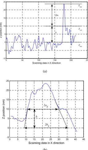
The protocol to extract these parameters is illustrated in Fig. 4, as follows:
Determination of global altitudes:
- altitude Ztop at the top of the highest asperity;
- Truncated altitude Zcut, calculated with the given
interference Dis for each sample: Zcut = Ztop - Dis.
The parameter Dis, which represents the contact deformation under the maximum experimental contact force (145 µN for Au-Au contact, 200 µN for Ru-Ru contact) [33], is determined on the basis of mechanical contact simulations,
-For Au-Au contact, get Dis = 12 nm -For Ru-Ru contact, get Dis = 8 nm.
(a)
(b)
Fig. 2. Topography of rough surfaces for samples in: (a) gold, (b) ruthenium
Then, for each asperity, extract or calculate: - altitude at the bottom of asperity Zbot;
- asperity height: h= Zcut - Zbot;
- tip radius of asperity, defined by the average of measurement in cross section X and Y: a= (aX + aY)/2;
- bottom radius of asperity, b = (bX + bY)/2;
- angle, 1=arctan (h/(b-a)).
0 20 40 60 0 10 20 30 -10 0 10 20 30 (a)
(b)
Fig. 3. Asperity profile, (a) view in perspective, (b) cone-truncated model
0 50 100 150 200 250 -10 -5 0 5 10 15 20 25
Scanning data in X direction
Z p o s it io n ( n m ) Zcut Zbot h Ztop Dis (a) 0 5 10 15 20 25 30 35 40 45 -5 0 5 10 15 20 25
Scanning data in X direction
Z p o s it io n ( n m ) 2aX 2bX h (b)
Fig. 4. Surface profile and the protocol to extract the parameters in X direction: (a) overview,(b) close view of an asperity
0 2 4 6 8 10 12 14 16 18 20 0 10 20 30 40 50 60 70 80 90 100 Load step R a d iu s o f s p o ts i n c o n ta c t (n m )
Fig. 5. Simulation results for Au-Au contact: spots radius in contact as a function of load steps (a loading-unloading cycle is applied with the maximum contact force of 145 µN at the 10th load step, i.e. 10 steps for loading and 10 steps for unloading, for more details see [32]).
TABLE II. GEOMETRICAL PARAMETERS OF ASPERITIES EXTRACTED FROM THE AFM SCANNING DATA OF SAMPLE IN GOLD Asperity Geometrical parameters
a (nm) h (nm) 2 (°) b (nm) 1 56.4 10 19.5 84.6 2 17 10 18.8 46.4 3 30.8 10 18.9 60.1 4 12.5 10 15.3 49 5 34 10 16 68.8 TABLE III. GEOMETRICAL PARAMETERS OF ASPERITIES EXTRACTED
FROM THE AFM SCANNING DATA OF SAMPLE IN RUTHENIUM Asperity Geometrical parameters
a (nm) h (nm) 2 (°) b (nm)
1 36.1 12 27.5 59 2 32.5 7 12 65 3 65.2 6 10.5 97.8 4 53 3 6 81.5
3) Extracted geometrical parameters
The geometrical parameters extracted are listed in TABLE II and III, for the sample in gold and in ruthenium respectively. The mechanical simulation results of the spots radius for the sample in Au are given in Fig. 5. Comparing the spots radius obtained by the two methods confirms the range of the radius: from tens to hundred or so of nanometers.
Extending the values in TABLE II and III, the ranges of the geometrical parameters in the following finite element (FE) model are given as:
- Radius: a = [13 nm – 130 nm]; - Height: h = [3 nm – 30 nm]; - Angle: 1 = [3° - 60°].
B. Finite Element Model of One Asperity
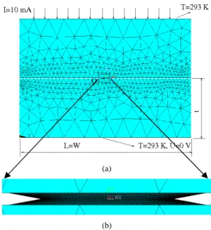
The FE model is built with commercial software package ANSYSTM of version 11.0. The bump of microswitches is simplified by a rectangular block with length (equal to width) of 3.5 µm and height of 1 µm (Fig. 6), the model considers only one asperity in contact firstly. The mesh is symmetrical to the plane (O, X, Y).
The 3-D 10 node coupled-field element SOLID227 is used in the simulations, with the degrees of freedom (DOF): temperature and voltage activated. The asperity region is meshed much finer while the volume of block is meshed gradually coarse.
Boundary conditions are set as follows (see Fig. 6):
- Temperature at the bottom and top surfaces of the model is constrained to ambient temperature T0= 293 K;
- Electrical current 10 mA is applied in the vertical direction at the top surface of upper volume;
- Free but uniform voltage is applied at the top surface of upper volume (with coupled degree of freedom Volt);
- Zero voltage is applied to the bottom surface of lower volume.
Thermoelectrical material properties are given in TABLE IV.
C. Regarding Multiple Asperities in Contact
Our previous mechanical simulations showed that there were about four to seven asperities which made contact under maximum contact force 145µN [32]. Also, a SEM micrograph showed that at most tens of asperities could make contact [34]. The number of asperities in our study then varies by n =1, 2, 4, 9 and 16.
Furthermore, all of the spots are assumed to have the same tip radii. For n asperities, the average tip radius an is calculated
by an=a1/n, where a1 is set as 130.4 nm, is the tip radius for one
asperity.
(a)
(b)
Fig. 6. Finite element modeling of an asperity: front view, (a) whole model, (b) zoom in the asperity
Fig. 7. Schema of nine asperities in contact: top view (on the square of 3.5×3.5 µm)
TABLE IV. THERMOELECTRICAL PROPERTIES FOR MATERIAL AU AND RU Properties Material Au Ru Electrical resistivity (1×m) 22.14×10 -9 76×10-9 Thermal conductivity (W/(m×K)) 318 117 Mean free path (nm) 38 10
The distance between spots for two asperities is half of the width of the rectangle, i.e. m= 1732 nm. For more than four asperities, the asperities are distributed evenly on a square grid, so as to define the same diameter d of contacting apparent area. Fig. 7 shows a schema for nine asperities.
Regarding the distribution of asperities, four asperities in contact are discussed as an example, the distance between asperities m varies in the range of 150 nm – 1732 nm.
IV. RESULTS AND DISCUSSIONS
A. One Asperity in Contact 1) Asperity tip radius
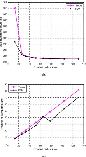
The reference model is built with the geometrical parameter of asperity 3 in TABLE III, i.e. a = 65.2 nm, 1 =10.5° and h = 6 nm.
The first parameter discussed is the asperity tip radius, which is varied in the range of 13 nm – 130 nm, without changing the space angle and asperity height constant. The simulations and theoretical results are shown in Fig. 8.
It is shown that, about constriction resistance, numerical results match very well with theoretical results for an asperity larger than 26 nm. However, there is a large discrepancy with a small asperity a = 13 nm. This suggests that the FE model can predict the constriction resistance precisely on the diffusive transport regime, but cannot model the ballistic effect. The same trend is also found for the maximum temperature.
0 20 40 60 80 100 120 140 0 0.5 1 1.5 2 2.5 3 3.5 Contact radius (nm) C o n ta c t re s is ta n c e ( Ω ) Theory FEM (a) d
0 20 40 60 80 100 120 140 292 294 296 298 300 302 304 306 308 310 312 Contact radius (nm) M a x im u m t e m p ra tu re ( K ) Theory FEM (b) 0 20 40 60 80 100 120 140 0 10 20 30 40 50 60 70 80 90 Contact radius (nm) P o s it io n o f T e m p M a x ( n m ) Theory FEM (c)
Fig. 8. Influence of asperity radius on (a) constriction resistance, (b) maximum temperature, (c) position of maximum temperature
(a)
(b)
Fig. 9. Simulation results for asperity radius a= 78 nm, close view of the asperity: (a) isothermal surfaces, (b) elements meshing and the position of the maximum temperautre
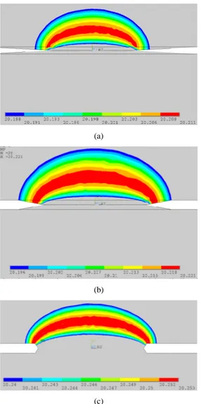
Fig. 9 (a) shows that the isothermal surfaces have the shape of quasi-hemisphere, and 2z should be found on the z-axis according to the definition (8). Since the elements in the numerical model are discrete, 2z is taken as the distance between the z-coordinate of the node nearest to the z-axis and the physical interface of the contact, i.e. the symmetrical surface of the FE contact model.
It is shown in Fig. 8 (c) that for the position of the maximum temperature, the numerical results match quite well with the analytical results. This is reasonable considering that Holm formula (8) did consider only the diffusive transport mode, which is also the only mode can predict the numerical model. However, the discrepancy between the theoretical and numerical results increases with larger asperities; and this may come from the coarse meshing in the volume (cf. Fig. 9 (b)).
2) Asperity angle
The simulations in this part are carried out with the contact radius and the asperity height remain constant as a=65.2 nm,
h=6 nm, and the angle of asperity varies in the range of 3° to
60°.
The results of Sano (Fig. 10 (a)) indicate an important effect of space angle on the constriction resistance: Rc increases
43% with the angle of 20° compared to 0°. As is shown schematically in Fig. 1, Sano considered that each electrode was infinite with the inclined line as the asymptote curve of the electrode surface. Instead, our model assumes that the cone has a defined height h. It is then reasonable that the calculated resistance by Sano is greater than that of estimated by our FE models.
Compared to the values calculated by Holm formula, the simulations results show a slight increase on the electrical resistance with the space angle, and the relative difference is only 9.4% for the space angle changing from 3° to 60°. For the most real contact surfaces, the average space angle of asperities are generally less than 20° [13], this will result in an increase on the electrical resistance at most 4.6% only.
As for the increase of temperature, which is the result of Joule heating by the contact resistance, rises 17.7% when angle rises from 3° to 60°.
Even the meshing is not fine enough, the position of maximum temperature as a function of angle shows a regular and interesting trend: it increases from 3° to 10.5°, and then decreases. The explication traces can be found in Fig. 11. The isothermal surfaces are within the asperity with small angle, and the warmest isothermal surface locates farther when the space angle becomes larger. However, when the space angle is large enough, the isothermal surfaces are expanding into the volume, and the warmest isothermal surface then is located closer to the physical interface with greater angle.
0 10 20 30 40 50 60 0.2 0.4 0.6 0.8 1 1.2 1.4 1.6
Space angle of contact (°)
C o n ta c t re s is ta n c e (Ω ) Formula Holm Formula Sano FEM (a) 0 10 20 30 40 50 60 293.19 293.2 293.21 293.22 293.23 293.24 293.25 293.26
Space angle of contact (°)
M a x im u m t e m p ra tu re ( K ) Theory FEM (b) 0 10 20 30 40 50 60 32 33 34 35 36 37 38 39 40 41 42
Space angle of contact (°)
P o s it io n o f T e m p M a x ( n m ) Theory FEM (c)
Fig. 10.Influence of space angle on (a) constriction resistance, compared with the model of Sano (1) and Holm (2), (b) maximum temperature, (c) position of maximum temperatue
(a)
(b)
(c)
Fig. 11.Distribution of temperature on the asperity proximity for one asperity in contact, with space angle of (a) 3°, (b) 10.5° and (c) 60°
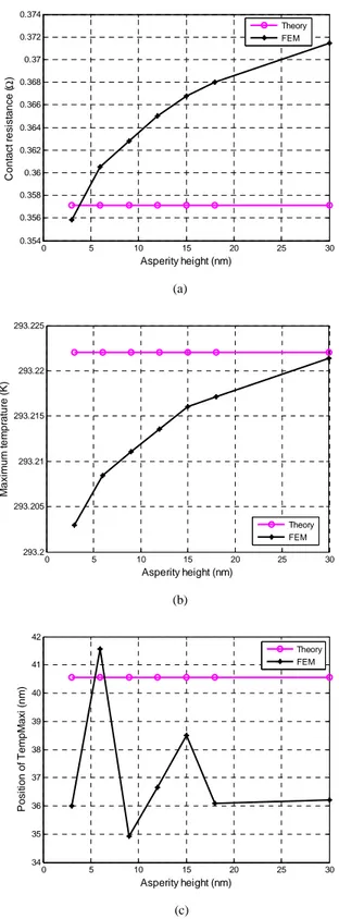
3) Asperity height
The asperity height varies in the range of 3 nm - 30 nm with the tip radius and the space angle of asperity constant as: a = 65 nm and 1 = 10.5 °.
It is shown in Fig. 12 that the contact resistance increases only 4.4% for asperity height varies from 3 nm to 30 nm, and also the increase of temperature increases slightly.
The position of maximum temperature varies in the range of 35 nm – 41.6 nm, and the discrepancy is acceptable compared to the theoretical value of 40.56 nm. However, again due to the coarse meshing in the block volume, no good conclusion can be made, and finer meshing may be required for further study.
0 5 10 15 20 25 30 0.354 0.356 0.358 0.36 0.362 0.364 0.366 0.368 0.37 0.372 0.374 Asperity height (nm) C o n ta c t re s is ta n c e (Ω ) Theory FEM (a) 0 5 10 15 20 25 30 293.2 293.205 293.21 293.215 293.22 293.225 Asperity height (nm) M a x im u m t e m p ra tu re ( K ) Theory FEM (b) 0 5 10 15 20 25 30 34 35 36 37 38 39 40 41 42 Asperity height (nm) P o s it io n o f T e m p M a x i (n m ) Theory FEM (c)
Fig. 12.Influence of asperity height on (a) constriction resistance, (b) maximum temperature, (c) position of maximum temperature
B. Multiple Asperities in Contact 1) Number of asperities
Regarding multiple spots in contact, TABLE V lists the asperities radii and the distances between them. The asperity
height and the space angle of asperity are set constantly as: h = 6 nm and 1 = 10.5°.
For the analytical calculation, as has been discussed for one asperity, the numerical simulations cannot model the ballistic effect, so the contact resistance is calculated with Holm formula (2), and furthermore, electrical interaction between asperities is neglected. So with the asperity radii an=a1/n, the
analytical constriction resistance keeps almost constant (Rth in
TABLE V).
While numerical models (RFE in TABLE V) predict that the
resistance increases with more asperities in contact. Indeed, with shorter distance between asperities, electrical interaction should be more significant. Yet the increase of electrical resistance remains small, rising 13% with 16 asperities compared to one asperity.
The total contact area, however, varies widely, and it can be seen that their values are almost inversely proportional to the number of asperities. Therefore, it can be deduced that the contact area cannot be calculated only from the measurement of the electrical resistance if the distribution and number of asperities are not known, as has been discussed in [25] and [29].
TABLE V. MULTI-ASPERITIES : COMPARISON BETWEEN NUMERICAL AND ANALYTICAL RESULTS
Number of asperities
Parameters and results
a (nm) Total contact area (nm2) Distance m (nm) Rth (3) RFE (3) 4z (nm) 1 130.4 17004 0.1882 0.1828 70.5 2 65.2 8502 1732 0.1882 0.1906 39.4 4 32.6 4251 1271 0.1882 0.1973 18.8 9 14.5 1892 648.3 0.1880 0.2055 8.5 16 8.15 1063 435 0.1882 0.2056 4.2
As for the location of maximum temperature, even with inaccuracy due to the coarse meshing in the volume, we can also conclude that with more asperities in contact, 2z becomes smaller with smaller asperity. This implies that the Joule heating concentrates closer to the proximity of asperities, and it will be easier for contact be fused at high current.
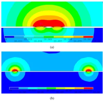
2) Distance between asperites
Fig. 13 shows the influence of distance between asperities on the constriction resistance and on the position of maximum temperature. The effect of distance on the constriction resistance becomes more important from the value of 1000 nm. The maximum temperature locates farther from the physical interface when the asperities are closer to each other. As can be seen in Fig. 14, the current interaction becomes more significant when asperities are closer to each other, and the isothermal surfaces are merged, and they are more like one large asperity, so the position of the maximum temperature becomes higher.
C. Comparison againt the experimental results
The experimental measurement in [23] showed that the Au/Ru bimetallic contact had the contact resistance of 1.9 1 at the contact force of 145 µN and the current of 1 mA. This value leads to the contact radius of 13 nm with the diffusive transport mode. However, according to the mechanical simulations, the contact radius is about 100 nm at 145 µN [32]. Since the mechanical simulations have been validated to be capable of predicting the contact mechanical behavior [35], it is likely that the discord on the contact radius, calculated by the mechanical simulations and the experimental resistances, comes from the insulating film on the contact surface, the modeling work on this concept will be presented in the following paper. 102 103 0.19 0.2 0.21 0.22 0.23 0.24 0.25 0.26
Distance between spots in contact (nm)
C o n ta c t re s is ta n c e ( Ω ) (a) 0 200 400 600 800 1000 1200 1400 1600 1800 18 19 20 21 22 23 24 25 26 27
Distance between spots in contact (nm)
P o s it io n o f m a x im u m t e m p e ra tu re ( n m ) Holm formula (7) FEM (b)
Fig. 13.Influence of distance between asperities on (a) constriction resistance, (b) position of the maximum temperature
(a)
(b)
Fig. 14.Distribution of temperature on the asperities proximity for 4 asperities in contact, with distance between asperities: (a) m= 150 nm, (b) m= 1271 nm
V. CONCLUSIONS
This paper proposed a 3-D geometrical model for the asperity of electrical contact of microswitches. A series of simulations were conducted to examine the impacts of three parameters in the 3-D model, namely, radius, asperity angle and height. As agreed to the conventional asperity model, the numerical model showed that the asperity tip radius had much more significant impact on the electrical resistance and the thermoelectrical phenomena, and the two other parameters only had significant influence when the asperity size became larger. Concerning multiple asperities in contact, with the contact resistance almost constant, more asperities tend to bring down the position of maximum temperature. Also, with the same number of asperities, shorter distance between asperities results in a higher electrical resistance and a higher position of the maximum temperature.
It should be emphasized that the numerical simulations could not model well the ballistic effect. For small asperities, the resistance was underestimated compared to the theoretical results.
ACKNOWLEDGMENT
H. Liu would like to thank the CSC (China Scholarship Council) for providing the finance support for PhD study.
REFERENCES
[1] D. Hyman and M. Mehregany, “Contact physics of gold microcontacts for MEMS switches,” Ieee Trans. Components Packag. Technol., vol. 22, no. 3, pp. 357 –364, 1999.
[2] A. Lumbantobing, L. Kogut, and K. Komvopoulos, “Electrical contact resistance as a diagnostic tool for MEMS contact interfaces,” J. Microelectromechanical Syst., vol. 13, no. 6, pp. 977 – 987, 2004.
[3] D. J. Dickrell and M. T. Dugger, “Electrical Contact Resistance Degradation of a Hot-Switched Simulated Metal MEMS Contact,” Ieee Trans. Components Packag. Technol., vol. 30, no. 1, pp. 75–80, 2007. [4] R. S. Timsit, “Electrical Conduction Through Small Contact Spots,”
Trans. Components Packag. Technol., vol. 29, pp. 727–734, 2006. [5] R. A. Coutu, J. R. Reid, R. Cortez, R. E. Strawser, and P. E. Kladitis,
“Microswitches with sputtered Au, AuPd,Au-on-AuPt, and AuPtCu alloy electric contacts,” Ieee Trans. Components Packag. Technol., vol. 29, no. 2, pp. 341–349, 2006.
[6] O. Rezvanian, M. A. Zikry, C. Brown, and J. Krim, “Surface roughness, asperity contact and gold RF MEMS switch behavior,” J. Micromechanics Microengineering, vol. 17, no. 10, pp. 2006–2015, Oct. 2007.
[7] N. Agraı1t, A. L. Yeyati, and J. M. van Ruitenbeek, “Quantum properties of atomic-sized conductors,” Phys.Reports, vol. 377, no. 2–3, pp. 81– 279, Apr. 2003.
[8] R. Holm, Electric Contacts-Theory and Applications, 4th edn. Berlin: Springer, 1967.
[9] Y. V. Sharvin, “A Possible Method for Studying Fermi Surfaces,” Sov. Phys. Jetp, vol. 21, p. 655, 1965.
[10] G. Wexler, “The size effect and the non-local Boltzmann transport equation in orifice and disk geometry,” Proc Phys Soc, vol. 89, pp. 927– 941, 1966.
[11] A. Mikrajuddin, F. G. Shi, H. K. Kim, and K. Okuyama, “Size-dependent electrical constriction resistance for contacts of arbitrary size: from Sharvin to Holm limits,” Mater. Sci. Semicond. Process., vol. 2, no. 4, pp. 321–327, Dec. 1999.
[12] M. Nakamura, “Constriction resistance of conducting spots by the boundary element method,” Ieee Trans. Components Hybrids Manuf. Technol., vol. 16, no. 3, pp. 339–343, 1993.
[13] Y. Sano, “Effect of space angle on constriction resistance and contact resistance for a point contact,” J Appl Phys, vol. 58, pp. 2654–2654, 1985.
[14] Y. Sano, “Effect of Space Angle on Constriction Resistance and Contact Resistance for the Case of Line Contact,” Ieee Trans. Components Hybrids Manuf. Technol., vol. CHMT-8, pp. 228–234, 1985.
[15] O. Rezvanian, C. Brown, M. A. Zikry, A. I. Kingon, J. Krim, D. L. Irving, and D. W. Brenner, “The role of creep in the time-dependent resistance of Ohmic gold contacts in radio frequency microelectromechanical system devices,” J. Appl. Phys., vol. 104, no. 2, pp. 024513–024513–5, Jul. 2008.
[16] B. D. Jensen, L. L.-W. Chow, K. Huang, K. Saitou, J. L. Volakis, and K. Kurabayashi, “Effect of nanoscale heating on electrical transport in RF MEMS switch contacts,” J. Microelectromechanical Syst., vol. 14, no. 5, pp. 935 – 946, Oct. 2005.
[17] A. Monnier, B. Froidurot, C. Jarrige, P. Testé, and R. Meyer, “A Mechanical, Electrical, Thermal Coupled-Field Simulation of a Sphere-Plane Electrical Contact,” Ieee Trans. Components Packag. Technol., vol. 30, pp. 787–795, 2007.
[18] H. Ghaednia, A. Rostami, and R. L. Jackson, “The Influence of Thermal Expansion and Plastic Deformation on a Thermo-Electro Mechanical Spherical Asperity Contact,” in 2012 IEEE 58th Holm Conference on Electrical Contacts (Holm), 2012, pp. 1 –7.
[19] K. Koibuchi and K. Sawa, “Numerical study on current and thermal distribution of electical contacts by FEM,” in 53th Holm Conference on, 2007.
[20] L. Per, “Numerical study of asperity distribution in an electrical contact,” in Preceedings of the 57th IEEE Holm Conference, 2011. [21] M. Leidner, H. Schmidt, M. Myers, and H. F. Schlaak, “A new
simulation approach to characterizing the mechanical and electrical qualities of a connector contact,” Eur. Phys. J. - Appl. Phys., vol. 49, no. 02, 2010.
[22] [22] M. Leidner, H. Schmidt, and M. Myers, “Simulation of the Current Density Distribution within Electrical Contacts,” in 2010 Proceedings of the 56th IEEE Holm Conference on Electrical Contacts (HOLM), 2010, pp. 1–9.
[23] A. Broué, A. Dhennin, P.-L. Charvet, P. Pons, N. B. Jemaa, P. Heeb, F. Coccetti, and R. Plana, “Multi physical characterization of micro contact materials for MEMS switches,” in 2010 Proceedings of the 56th IEEE Holm Conference, 2010.
[24] F. Ke, J. Miao, and J. Oberhammer, “A Ruthenium-Based Multimetal-Contact RF MEMS Switch With a Corrugated Diaphragm,” J. Microelectromechanical Syst., vol. 17, no. 6, pp. 1447 –1459, Dec. 2008.
[25] J. A. Greenwood, “Constriction resistance and the real area of contact,” Brit J. Appl Phys., vol. 17, p. 1621, 1966.
[26] L. Boyer, S. Noel, and F. Houze, “Constriction resistance of a multispot contact: an improved analytical expression,” Ieee Trans. Components Hybrids Manuf. Technol., vol. 14, no. 1, pp. 134–136, 1991.
[27] R. D. Malucci, “Multispot model of contact based on surface features,” in 36th IEEE Holm Conference on Electrical Contacts, 1990.
[28] R. D. Malucci, “The Impact of Spot Size and Location on Current Density,” in 2009 Proceedings of the 55th IEEE Holm Conference on Electrical Contacts, 2009, pp. 208–213.
[29] M. Myers, M. Leidner, H. Schmidt, and H. Schlaak, “Extension and Experimental Verification of a New ‘First Contact’ Method to Model Performance of Multilayer Contact Interfaces,” in Proceedings of the 54th IEEE Holm Conference on Electrical Contacts, 2008, 2008, pp. 66 –73.
[30] M. Myers, M. Leidner, and H. Schmidt, “Effect of Contact Parameters on Current Density Distribution in a Contact Interface,” in 2011 IEEE 57th Holm Conference on Electrical Contacts (Holm), 2011, pp. 1–9. [31] F. Pennec, D. Peyrou, D. Leray, P. Pons, R. Plana, and F. Courtade,
“Impact of the Surface Roughness Description on the Electrical Contact Resistance of Ohmic Switches Under Low Actuation Forces,” Ieee Trans. Components Packag. Manuf. Technol., vol. 2, no. 1, pp. 85 –94, 2012.
[32] H. Liu, D. Leray, P. Pons, S. Colin, and A. Broué, “Finite element based surface roughness study for ohmic contact of microswitches,” in IEEE 58th Holm Conference on Electrical Contacts, 2012.
[33] A. Broué, “Analyse multi physique des sources de défiabilisation du microcontact électrique à destination des interrupteurs MEMS,” Univ de Toulouse, 2012.
[34] S. Majumder, N. E. McGruer, G. G. Adams, A. Zavracky, P. M. Zavracky, R. H. Morrison, and J. Krim, “Study of contacts in an electrostatically actuated microswitch,” in Proceedings of the Forty-Fourth IEEE Holm Conference on Electrical Contacts, 1998, 1998, pp. 127 –132.
[35] H. Liu, D. Leray, P. Pons, S. Colin, A. Broué, and J. Martegoutte, “Validation of finite element structural simulation for ohmic microcontacts,” in Proceedings of Eurosensors XXV, 2011.
![Fig. 1. Asperity model suggested by Sano [13]](https://thumb-eu.123doks.com/thumbv2/123doknet/11598430.299193/2.892.563.763.841.965/fig-asperity-model-suggested-sano.webp)