HAL Id: tel-01508918
https://pastel.archives-ouvertes.fr/tel-01508918
Submitted on 15 Apr 2017HAL is a multi-disciplinary open access archive for the deposit and dissemination of sci-entific research documents, whether they are pub-lished or not. The documents may come from teaching and research institutions in France or abroad, or from public or private research centers.
L’archive ouverte pluridisciplinaire HAL, est destinée au dépôt et à la diffusion de documents scientifiques de niveau recherche, publiés ou non, émanant des établissements d’enseignement et de recherche français ou étrangers, des laboratoires publics ou privés.
low-temperature silicon epitaxy by plasma enhanced
chemical vapor deposition
Farah Haddad
To cite this version:
Farah Haddad. Transmission electron microscopy study of low-temperature silicon epitaxy by plasma enhanced chemical vapor deposition. Materials Science [cond-mat.mtrl-sci]. Université Paris Saclay (COmUE), 2016. English. �NNT : 2016SACLX107�. �tel-01508918�
NNT : 2016SACLX107
T
HESE DE DOCTORAT
DE
L’U
NIVERSITE
P
ARIS
-S
ACLAY
PREPAREE A
“
L
’E
COLE
P
OLYTECHNIQUE
”
E
COLED
OCTORALE N° 573
Interfaces : approches interdisciplinaires / fondements, applications et innovation
Spécialité de doctorat : Physique
Par
Mme Farah Haddad
Transmission electron microscopy study of low-temperature silicon epitaxy by
plasma enhanced chemical vapor deposition
Thèse présentée et soutenue à « Palaiseau », le « 14 décembre 2016 » :
Composition du Jury :
M. Gilles Patriarche
Mme Sabine Lay-Dietrich M. Pierre Ruterana
Mme Agnès Granier M. Jean-Luc Maurice
M. Pere Roca i Cabarrocas
Président Rapporteur Rapporteur Examinatrice Directeur de thèse Co-directeur de thèse DR CNRS, C2N DR CNRS, INPG-PHELMA DR CNRS, ENSICAEN DR CNRS, IMN DR CNRS, Ecole Polytechnique DR CNRS, Ecole Polytechnique
iv
Acknowledgment
First and foremost, I thank God for providing me this opportunity and granting me the capability to proceed successfully. The present manuscript would not have been possible without the help, encouragement and support of many persons. I thank all of them and I present them all my gratitude.
I am deeply grateful to all members of the jury for agreeing to read the manuscript and to participate in the defense of this thesis. Very special thanks go to Jean-Luc Maurice, my supervisor, for his kind guide, support, help, encouragement and… much more. I appreciate the freedom and confidence he provided me. He was always there to answer my questions and discuss whenever I needed. I express my gratitude to Pere Roca i Cabarrocas, my co-supervisor and the head of LPICM, for his constant encouragement and relevant advices, despite his very busy agenda; I admire his passion during scientific discussions.
I would like to thank my colleague Prabal Goyal who made the growth experiments for me, he gave me a lot of samples to study and characterize and was always ready to make new ones with pleasure. I appreciate his honesty and care in our collaboration. I would like to thank Ronan Léal for his collaboration and for the growth experiments. I cannot forget Jean-Christophe Dornstetter who was ready to discuss about microcrystalline and epitaxial silicon at anytime. Thanks to him, I made a background on this topic during the beginning of my thesis. I confess he was my inspiration to do some studies.
I would like to acknowledge Erik Johnson, Holger Vach and François Siva for their valuable discussions on some results. I would like to thank Martin Foldyna for his advices and coffee breaks. I express my gratitude to the CIMEX team, especially Ileana Florea, Pierre-Eugène Coulon, Eric Larquet and Mathias Kobylko for helping me working on the TEM when it had problems. I extend my sincere thanks to all members of LPICM, especially Huda Haddad, Paul Narchi, Mariam Ezzedine, Fatima Jardali, Fatima Bouaniss, Warda Hadouchi, Mutaz Al-Ghzaiwat, Angelo Grimaldi, Xin Yang Wang, Wanghua Chen, Loic Loisel, Bastien Bruneau and Romain Cariou for making LPICM a nice play to work.
A special thank goes to Pierre Legrain (for his confidence and support), Michel Rosso, François Ozanam and Fouad Maroun, I will never forget their support during my first year of PhD.
Without the support of my mother, my father, my brothers, and my parents-in-law, their prayer for me was what sustained me so far. I acknowledge their confidence and love. Finally, I would like to extend my warmest thanks to my lovely husband who is always supporting and encouraging me especially in the most difficult situations. Caring and tender, he is illuminating my life.
v
Résumé
Cette thèse s’intéresse à la croissance épitaxiale à basse température (~200°C) des couches minces de silicium par dépôt chimique en phase vapeur assisté par plasma (PECVD), pour des applications aux cellules solaires. L’objectif de départ était de mieux comprendre cette croissance épitaxiale, en utilisant la microscopie électronique en transmission (MET) comme principal outil expérimental. Afin de réussir les observations MET en coupe, une étape d’amincissement est indispensable pour avoir un échantillon transparent aux électrons.
D’abord, nous avons étudié les premiers stades de cette croissance épitaxiale en chimie tetrafluorure de silicium, hydrogène et argon (SiF4/H2/Ar) ou en chimie silane et hydrogène (SiH4/H2), en menant une
série de dépôts courts – quelques dizaines jusqu’à quelques centaines de secondes – sur différents types de substrats. Nous avons utilisé comme substrats des wafers de Si (100), des wafers de Si (111), des wafers d’arséniure de gallium GaAs (100), des grilles MET de Si (100), ou des grilles MET de cuivre avec membrane de carbone amorphe). Nous avons établi une corrélation entre les images MET de coupes et de vues planes et les mesures d’ellipsométrie in-situ. Nous avons discuté les mécanismes de croissance en nous basant sur l’hypothèse de la croissance traditionnelle à base de radicaux et ions et l’hypothèse (relativement nouvelle) reposant sur la fonte des particules générées par le plasma au moment de l’impact avec le substrat.
De plus, pour comprendre comment l’épitaxie par PECVD à basse température se maintient, nous avons étudié comment elle se brise ou se perd. Pour cela, des expériences de perte d’épitaxie ont été visées en augmentant soit la puissance de la source radiofréquence (RF), soit le flux d’hydrogène, pour une chimie SiF4/H2/Ar. Dans les deux cas, le mécanisme de brisure d’épitaxie fait intervenir des macles et des
fautes d’empilement qui interrompent la configuration épitaxiale. Après avoir comparé nos résultats avec ceux de la littérature, nous proposons que la brisure d’épitaxie du silicium passe par une rugosification de surface (mise en évidence par le signal de l’ellipsométrie in-situ pour tous les échantillons ayant subi une brisure d’épitaxie) qui introduit les macles et les fautes d’empilement. Grâce à cette nouvelle compréhension de la brisure d’épitaxie, nous proposons quelques moyens pour maintenir l’épitaxie pour de plus grandes épaisseurs.
En outre, nous avons observé une fascinante quasi-symétrie cinq dans les diagrammes de diffraction pour ces couches et aussi pour d’autres élaborées par un plasma de chimie SiH4/H2/HMDSO/B2H6/Ar.
Nous avons attribué une telle symétrie à une brisure d’épitaxie par l’intermédiaire d’un maclage multiple. Nous avons développé une méthode d’analyse quantitative qui permet de : (1) discriminer les positions de maclage de celles du microcristal aléatoire dans les diagrammes de diffraction, (2) estimer
vi le nombre des opérations de maclage et (3) évaluer la contribution de chaque ordre de maclage. Nous avons aussi discuté quelques raisons probables pour l’incidence du maclage et du maclage multiple sous forme de symétrie cinq. La tendance du système à aligner les plans {111} presque parallèlement à l’axe de croissance nous semble un facteur majeur pour l’apparition d’une telle symétrie.
Finalement, une importante réalisation pour le monde de la MET, durant ce travail doctoral, est l’optimisation de la préparation traditionnelle d’échantillon ou polissage par la méthode du tripode. Nous l’avons transformée d’une méthode longue et ennuyeuse en une méthode rapide qui devient compétitive par rapport à la technique du FIB relativement chère. Un des secrets de cette réalisation est la superposition de plusieurs échantillons dans un même sandwich (voire 4 échantillons au lieu de 2). Un autre secret est le polissage de la première face de plusieurs sandwiches (voire 4 sandwiches ou 16 échantillons) simultanément, alors que le polissage de la deuxième face de chaque sandwich est fait séparément (étape très critique et sensible) ; Ceci réduit énormément le temps d’amincissement d’échantillons.
vii
Contents
Acknowledgment ... iv Résumé ... v Contents ... vii List of figures ... xList of tables ... xviii
List of acronyms ... xix
Chapter 1. General introduction ... 1
1.1. Solar energy ... 2
1.2. Silicon photovoltaic technology ... 4
1.3. Low-temperature Si epitaxy by plasma enhanced chemical vapor deposition... 5
1.3.1. Motivation ... 5
1.3.2. History ... 6
1.3.3. Some challenges ... 7
1.4. SiF4/H2/Ar plasma chemistry ... 9
1.5. SiH4/H2/HMDSO/B2H6/Ar plasma chemistry... 10
1.6. Framework of this thesis ... 11
1.6.1. Focus on understanding epitaxial growth of Si thin films by LT-PECVD ... 11
1.6.2. Aim and outline of this PhD thesis ... 14
Chapter 2: Growth and characterization methods ... 16
2.1. Plasma enhanced chemical vapor deposition (PECVD) ... 17
2.1.1. Fundamentals of PECVD ... 17
2.1.2. Brief description of the reactors ... 18
2.2. Characterization methods ... 20
2.2.1. Transmission electron microscopy ... 20
2.2.2. Ellipsometry ... 31
viii
3.1. Introduction ... 35
3.2. SiF4/H2/Ar plasma (CLUSTER reactor) ... 37
3.2.1. Evidence for the presence of a transient regime- long deposition ... 37
3.2.2. Short deposition on Si (100) wafers ... 41
3.2.3. Short deposition on TEM copper grids with carbon membrane ... 43
3.3. SiH4/H2 plasma (ARCAM reactor) ... 46
3.3.1. Growth morphology on Si (100), GaAs (100) and Si (111) wafers - short depositions ... 47
3.3.2. Short deposition on Si (100) TEM grids ... 49
3.4. Discussion ... 51
3.4.1. Hypothesis of growth mediated by atoms, radicals or ions ... 52
3.4.2. Hypothesis of growth mediated by plasma generated particles ... 56
3.4.3. Growth mechanisms: an open discussion ... 62
3.4.4. Effect of the substrate ... 64
3.5. Summary and perspectives ... 65
Chapter 4. Epitaxy breakdown using SiF4/H2/Ar plasma ... 66
4.1. Introduction ... 67
4.2. Intentional epitaxy breakdown with increasing the RF power ... 69
4.2.1. RF power of 20 W on Si (100) substrate ... 69
4.2.2. RF Power of 25 W on Si (100) and Si (111) substrates ... 76
4.2.3. Summary of the results – epitaxy and breakdown by increasing the RF power ... 82
4.3. Intentional epitaxy breakdown with increasing the H2 flow rate ... 84
4.3.1. Hydrogen flow rate of 2 sccm on Si (100) wafers ... 84
4.3.2. Hydrogen flux of 3 sccm on Si (100) wafers ... 90
4.3.3. Summary of results - epitaxy and breakdown by increasing the H2 flow rate ... 93
4.4. Discussion ... 95
4.4.1. Breakdown by power ... 96
4.4.2. Breakdown by hydrogen ... 100
4.5. Summary and perspectives ... 105
ix
5.1. Introduction ... 107
5.1.1. Overview of twinning and fivefold symmetry in literature ... 107
5.1.2. Fivefold symmetric diffraction patterns in Si thin films ... 108
5.2. Twinning in Si films promoted by epitaxy breakdown from SiF4/H2/Ar plasma... 111
5.2.1. Epitaxy breakdown by increasing the RF power ... 112
5.2.2. Epitaxy breakdown caused by increasing the H2 flow rate ... 121
5.3. Twinning in Si films promoted by epitaxy breakdown from SiH4/H2/HMDSO/B2H6/Ar plasma ... 126
5.3.1. Effect of the substrate ... 127
5.3.2. Effect of HMDSO flow rate ... 131
5.3.3. Number of twin operations ... 133
5.3.4 MT and microcrystalline contributions ... 133
5.3.5. Chemical analysis ... 136
5.4. Discussion ... 138
5.4.1. Growth twins and fivefold symmetry ... 138
5.4.2. Origin of twinning and multiple twinning ... 139
5.4.3. Twinning and epitaxy breakdown ... 143
5.4.4. Effect of the seed orientation on twinning - Si (100) vs Si (111) ... 148
5.5. Summary and perspectives ... 150
Chapter 6. Conclusion and perspectives ... 151
6.1. Contribution to the research field ... 152
6.2. Perspectives for future work ... 153
References ... 155
x
List of figures
Figure 1. Estimated renewable energy share of global final energy consumption, 2014 [2] ... 2
Figure 2. Average annual growth rates of renewable energy capacity and biofuels production from end 2010 to end 2015 [2] (*CSP for concentrating solar power). ... 3
Figure 3. Solar PV global capacity, by country/region, from 2005 to 2015 [2]. ... 3
Figure 4. Market share of different PV technologies from 1980 to 2015 [3] ... 4
Figure 5. Transmission electron microscopy image showing crystalline parts embedded in an amorphous matrix: this is polymorphous Si [29] ... 8
Figure 6. Structure of hexamethyldisiloxane (HMDSO) ... 11
Figure 7. Diamond cubic crystal structure of Si. ... 12
Figure 8. Silicon crystal seen along the <110> direction ... 13
Figure 9. ABC stacking in a face centered cubic crystal ... 14
Figure 10. Schematic view of the potential distribution in a capacitively coupled plasma in a RF discharge. The substrate is grounded and the RF voltage is applied to the RF electrode, for most of the cases. ... 18
Figure 11. Photos of CLUSTER [51], PHILIX [31] and ARCAM [51] reactors located at PICM laboratory. ... 19
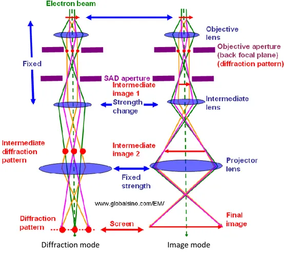
Figure 12. The transmission electron microscope compared with a slide projector ... 21
Figure 13. Schematic ray diagram showing a comparison of the lens conditions between diffraction and image modes. ... 23
Figure 14. Bragg diffraction: two beams approach a crystalline solid and are scattered off two different atoms within it. Constructive interference occurs when the path difference between the two beams (2d.sinθ) is equal to an integer multiple of the radiation wavelength. Note that, in the case of TEM, θ is of the order of a few mrad (≈1 degree)... 23
Figure 15. (a) Thickness map and (b) its profile for an epitaxial sample prepared by polishing and ion milling. The thickness of the sample is around 45 nm ... 24
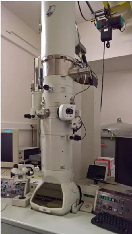
Figure 16. The JEOL 2010F microscope used in this doctoral work in the CIMEX. ... 25
Figure 17. Procedure before polishing: (a) cutting the sample with a diamond tip into slices and glue them face to face, (b) cutting them into thinner slices (the dashed lines indicate further slicing) and (c) gluing one slice on the glass of the tripod polisher. ... 26
Figure 18. Wire saw system for a high precision cutting of a sample into small slices. ... 26
Figure 19. (a) Different abrasive disc, each one corresponds to a granulation size: 30, 15, 6, 3, 1 and 0.5 μm from left to right. (b) Polishing system ... 27
Figure 20. Each color corresponds to an abrasive disc characterized by its granulation size. Transitional thicknesses to move from one abrasive disc to another are: 125, 70, 35, 6, 3, 1 and 0.5 μm. ... 27
xi
Figure 22. TEM image showing an amorphized region in the thinnest part as indicated by the arrow. The dark
regions correspond to twinned monocrystalline domains. ... 29
Figure 23. Copper grid covered by a carbon membrane ... 30
Figure 24. (a) Plan view and (b) cross-section view of the Si (100) TEM grid... 31
Figure 25. Schematic of ellipsometry principle [57] ... 31
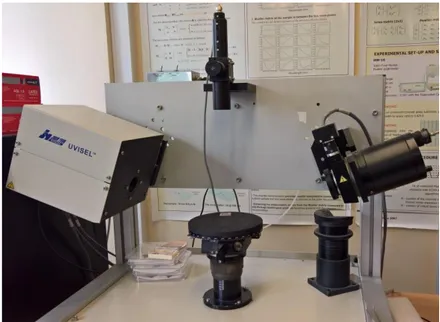
Figure 26. Photo of the ex-situ experimental setup at LPICM ... 33
Figure 27. Cross-section TEM image of sample C1 (long deposition) showing defects at the interface and island shapes on top of the epitaxial film. ... 37
Figure 28. HRTEM image of sample C1 showing the high quality epitaxy. ... 38
Figure 29. In-situ ellipsometry for deposition times t=0, 90 and 450 s. A minimum intensity at 4.2 eV is reached at 90 s, and then a stabilization occurs for t ≥ 1000 s. ... 38
Figure 30. Time evolution of the imaginary part of the pseudo-dielectric function measured at 4.2 eV (in blue) and 3.4 eV (in red). The stars indicate where the growth was stopped for the TEM samples discussed in section 3.2.2. ... 39
Figure 31. Evolution of the plasma potential with deposition time. ... 40
Figure 32. Cross-section TEM images of (100) c-Si wafers exposed to an epitaxial plasma for (a) 12 s, (b) 90 s and (c) 240 s. ... 42
Figure 33. Cross-section HRTEM images of a (100) c-Si wafers exposed to an epitaxial plasma for (a) 12 s, (b) 90 s and (c) 240 s. ... 42
Figure 34. (a) and (b) Low resolution TEM images of the deposition on the carbon membrane (for 90 s). (c) Diffraction pattern recorded on a zone of (b) including the large islands. ... 44
Figure 35. (a) Carbon map, (b) silicon map and (c) image combining silicon in red and carbon in green for the deposition on TEM copper grid for a deposition time of 90 s. ... 44
Figure 36. TEM images of the deposition on the carbon membrane corresponding to 12 s (a), 90 s (b) and 240 s (c). (a) shows dendritic aggregation of particles (with particle size of 12-25 nm), (b) shows spherical aggregation (~ 50 nm) and particles (~ 25 nm) aggregating in defective dendritic shapes and (c) shows big aggregates (110 - 200 nm). ... 45
Figure 37. TEM image showing the growth on a Si (100) wafer for deposition time of 8 s. ... 47
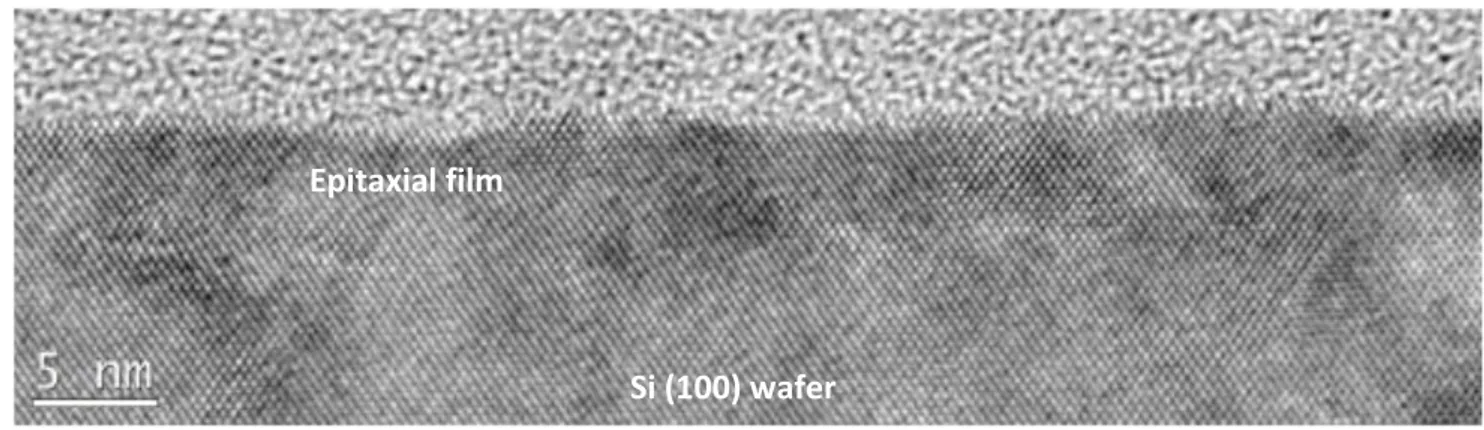
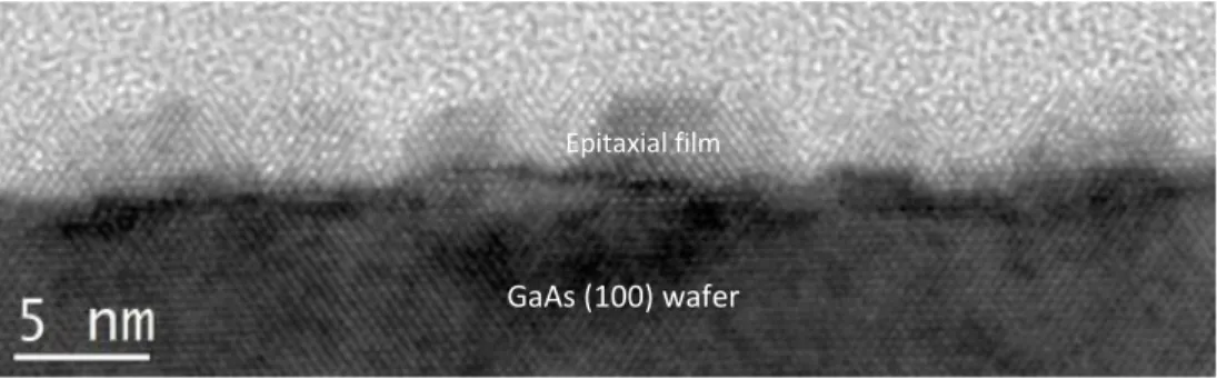
Figure 38. TEM image showing the growth on a GaAs (100) wafer for a deposition time of for 8 s. ... 48
Figure 39. TEM image illustrating the growth for 8 s on Si (111) wafer, it shows an amorphous film having a thickness around 5 nm. ... 48
Figure 40. TEM images recorded on the Si (100) grids near the edges of the windows showing contamination on the membrane before any deposition. ... 49
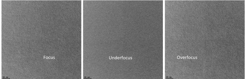
Figure 41. A series of TEM images of the Si membrane showing a smooth surface for (a) focused image, (b) underfocused image and (c) overfocused image (∆f= ± 56 nm). ... 49
Figure 42. A series of TEM images (focused, underfocused and overfocused, ∆f= ± 35 nm) corresponding to deposition for 8 s on Si (100) grids. ... 50
xii
Figure 43. TEM images showing crystalline islands found on Si (100) grids, they have size in the range of 10-20 nm ... 50 Figure 44. TEM images of the deposition on the Si grids. Few islands up to 80 nm in width are found, they are
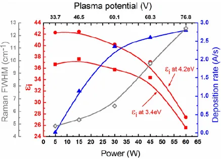
not uniformly distributed on the grids. ... 51 Figure 45. Growth modes at low temperature [78] ... 53 Figure 46. Evolution of the deposition rate,<εi> 3.4 and 4.2 eV and the Raman full width at half maximum as
a function of the plasma potential and power [65]. ... 55 Figure 47. Map of stress component 𝛔yy as simulated by Moras et al. [69]; tensile stress is represented in red
and compressive stress in blue. ... 56 Figure 48. Time evolution of the pressure, the DC bias between the electrodes and the real (ε1) and imaginary
(ε2) parts of the pseudo-dielectric function spectra measured at 3.4 eV, in the work of Schmidt et al.
[84]. An initial transient stage is detected at a power of 10 W due to particle formation, this is not the case at 3 W where no particles are formed. ... 59 Figure 49. TEM images recorded on carbon membrane showing crystalline particles having a diameter of 5 to
10 nm, these images are taken from the study of (a) Dornstetter [31] and (b) Johnson et al. [96]. ... 63 Figure 50. The growth conditions for the films presented in this chapter: two series of depositions were
carried out starting from the reference film, by increasing either the RF power or the H2 flow rate... 68
Figure 51. (a) Low magnification and (b) high resolution TEM images of the reference film obtained at a RF power of 15 W and a H2 flow rate of 1 sccm. The microstructure reveals a thickness of 750 nm of high
quality epitaxy that is almost free of defects. ... 69 Figure 52. TEM image of the film deposited using a RF power of 20 W and a H2 flow rate of 1 sccm. The black
dotted circles indicate the areas selected for the EDPs shown in Figure 53. Numbers are attributed to each area. ... 70 Figure 53. (a), (b) and (c) TEM images showing the areas selected for the EDPs shown in (d), (e) and (f),
respectively. (d) shows a perfect monocrystalline structure in region #1, (e) shows the monocrystalline orientation of the wafer (circled in red), twin orientations (indicated by yellow arrows), random microcrystalline orientations and amorphous contribution, in region #2. (f) is somehow similar to (e) but with a larger contribution of random microcrystalline, in region #3. ... 71 Figure 54. Profile of the blue rectangle in Figure 53(e) showing a small peak related to amorphous contribution
in the film. It corresponds to the diffused part between 220 and 311 rings. ... 71 Figure 55. HRTEM image confirming epitaxial growth in the beginning of the film: {111} planes are continuous
from the wafer to the film across the interface. ... 72 Figure 56. TEM image showing a high defect density after a certain thickness of epitaxial growth ... 73 Figure 57. Time evolution of the imaginary part of the pseudo-dielectric function <εi> measured at 4.2 eV, for
the sample deposited using a RF power of 20 W and a H2 flow rate of 1 sccm. ... 74
Figure 58. Decomposition of the film deposited at 20 W and 1 sccm of H2 flow rate, into four parts in the light
xiii
Figure 59. Plasma potential as a function of the deposition time for the film grown using a RF power of 20 W and a H2 flow rate of 1 sccm. ... 75
Figure 60. TEM image of the film deposited using a RF power of 25 W and a H2 flow rate of 1 sccm. ... 76
Figure 61. HRTEM image revealing epitaxy in the beginning of the film deposited using a RF power of 25 W and a H2 flow rate of 1 sccm. ... 77
Figure 62. HRTEM image showing a V-shaped defect formed within the monocrystalline matrix in the film. (b) and (c) are FFTs performed on the matrix and on the defective region, respectively. ... 78 Figure 63. (a) HRTEM image taken from the top of the film, (b) EDP recorded on the top of the film including
an area of 210 nm in diameter and dominated by monocrystalline and twin orientations (c) FFT corresponding to the red square showing microcrystalline and amorphous contributions. ... 78 Figure 64. In-situ ellipsometry measurements monitoring the evolution of the film growth. ... 79 Figure 65. Plasma potential as a function of the deposition time for the film deposited using a RF power of 25
W and a H2 flow rate of 1 sccm. ... 79
Figure 66. (a) TEM image of the sample deposited on Si (111) wafer using a RF power of 25 W and a H2 flow
rate of 1 sccm. The region of the film near the interface is enlarged in (b), it shows an epitaxial growth for the first 25 nm of the film growth. ... 81 Figure 67. (a) EDP taken from the white dotted circle in Figure 66(a), it shows the presence of the
monocrystalline wafer orientation (111 spots in red circles), twin orientations (indicated by arrows), random microcrystalline orientations and amorphous contribution. (c) EDP taken from the top of the film, it shows the presence of microcrystalline and amorphous phases. ... 81 Figure 68. FFTs performed inside the flame and outside it. The dark region corresponds to monocrystalline
and twin orientations, whereas the brighter is composed of amorphous and microcrystalline phases. 82 Figure 69. Summary of images corresponding to epitaxy (a) and epitaxy breakdown (b) and (c) for samples
deposited on Si (100) using a H2 flow rate of 1 sccm and different RF powers (15 W in (a), 20 W in (b)
and 25 W in (c)). ... 83 Figure 70. Description of epitaxy breakdown and epitaxy comeback mechanisms, on the basis of the TEM
observations in this chapter. Epitaxy breakdown occurs by (i) twinning followed by (ii) formation of a microcrystalline and amorphous phase. Twinning can be reversible and so epitaxy comeback is sometimes possible. ... 83 Figure 71. TEM images of the sample deposited on Si (100) using a RF power of 15 W and a H2 flow rate of 2
sccm; (b) corresponds to a thinner region of the foil. White dotted circles in (b) indicate the areas selected for the EDPs shown in Figure 72. Numbers refer to defects discussed in the text. ... 85 Figure 72.Diffraction patterns recorded on a region including (a) the wafer and the film and (b) the top of the
film, as indicated by the white dotted circles of Figure 71. ... 85 Figure 73. Defects numbered 1 in Figure 71(b) exhibiting Moiré fringes (due to stacking faults and twins). The
xiv
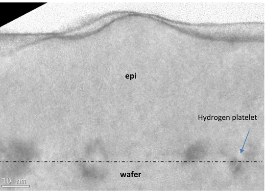
Figure 74. Defects numbered 2 are platelets following {111} planes and having a size of the order of 10 nm. In the inset, arrows indicate the presence of a lot of platelets within the film... 87 Figure 75. Defects numbered 3 are indicated by arrows, these are stacking faults following {111} plane and
displaying a strange contrast. They could correspond to dislocations decorated with hydrogen. ... 87 Figure 76. HRTEM image (a) and its associated diffractogram (b) where we selected (using masks of 0.7nm-1
in diameter) two 111 spots to obtain the filtered images in (c), (d), (e) and (f). Yellow arrows point at lattice distortions and the red ones at dislocations. ... 88 Figure 77. Selection of two 200 spots in the diffractogram (a) to form the filtered image (b). ... 89 Figure 78. In-situ ellipsometry measurements monitoring the evolution of the film deposited using a RF power
of 15 W and a H2 flow rate of 2 sccm. ... 90
Figure 79. TEM image of the sample deposited on Si (100) using a RF power of 15 W and a H2 flow rate of 3
sccm. ... 91 Figure 80. HRTEM image of the interface exhibiting some defects which are most likely hydrogen platelets. ... 91 Figure 81. (a) TEM image showing the same crystalline structure in the first 20 nm of the film and in the wafer,
then V-shaped defects appear initiating a highly defective region. (b) TEM image recorded on a thinner region of the TEM foil allowing us to better visualize the defects. ... 92 Figure 82. TEM image of the defective region, it corresponds to a highly twinned structure as shown by the
EDP in the inset. ... 92 Figure 83. In-situ ellipsometry monitoring the evolution of the film structure deposited using a RF power of
15 W and a H2 flow rate of 3 sccm. ... 93
Figure 84. Summary of images corresponding to (a) epitaxy, (b) defective epitaxy and (c) epitaxy breakdown for films deposited using a RF power of 15 W and different H2 flow rate: 1, 2 and 3 sccm respectively.
... 94 Figure 85.TEM images showing epitaxy breakdown for germanium Ge (100) layers deposited by LT-MBE for
substrate temperatures of 95°C (a) and 135°C and (b) from the work of Bratland et al. [103]. They both show critical thicknesses h1 and h2, where h1 defines the onset of epitaxial breakdown and h2 defines
the entire film transformation from epitaxial to amorphous. (c) Schematic illustration revealing the evolution of the microstructure and surface morphology. ... 97 Figure 86. Time evolution of the pseudo-dielectric function at 4.2 eV and the plasma potential while increasing
the RF power from 15 W to 21 W [80]. <εi> is stable when the plasma potential is below 61 V but
decreases abruptly above 61 V. ... 100 Figure 87. Schematic illustration of the hydrogen platelet generation and evolution according to Hochbauer
[118]. ... 102 Figure 88.TEM images of Si films showing stacking faults appearing after a certain thickness of epitaxial
xv
81), were attributed to a buildup of roughness caused by the adsorbed hydrogen through reducing surface diffusion. ... 103 Figure 89. Electron diffraction pattern along the [0-11] zone axis displaying a fivefold symmetry (sample
prepared with 0.45 sccm of HMDSO, see section 5.3) ... 108 Figure 90. (a) HRTEM image, recorded in the [0-11] zone axis, of the same layer as that imaged in Figure 89(b)
FFT of (a), (c) selection of five grain orientations and (d) colored image constructed from the IFFTs of orientations 1, 3 and 5. ... 110 Figure 91. The growth conditions for the films presented in this chapter: two series of depositions were
carried out starting from the reference film, by increasing either the RF power or the H2 flow rate. The
substrates used are Si (100) and Si (111), they are indicated for each film. ... 112 Figure 92. Schematic representation of the monocrystalline orientation of the substrate in black circles and
the allowed twin positions in red (anticlockwise) and blue (clockwise) spots for 111 ring. The zone axis is [0-11] and the growth axis is vertical. The order of twinning is indicated for each spot. Orders marked by * refer to twinning of the plane family associated with the spots at 70.53° and 250.53°, the others refer to that associated with spots at 0 and 180°. Only three orders of twinning are illustrated for visibility. ... 114 Figure 93. (a) EDP recorded on the MT part for the film deposited on Si (100) at 20 W, (b) azimuthal projection
of (a), the black shape is caused by the beam-stopper used while recording the EDP. (c) Profile of 111 reflections deduced from (b). M and M’ refer to spots of the monocrystalline grain (angles at 0 and 250.53° in Figure 92) and t refers to twin positions. The horizontal lines indicate the angles formed by the peak M and peaks attributed to a certain order of twinning about M situated at 0. ... 115 Figure 94. TEM images of the film deposited at 20 W: (a) shows the epitaxial and twinned parts of the film
displaying different contrasts. A “zigzag” intermediate line separating these two parts is shown in (b) where V-shaped defects are noticeable. ... 116 Figure 95.TEM images showing the twinned part (or MT part) around the zigzag line for the Si films deposited
using a RF power of 25 W on (a) Si (100) and (b) Si (111) substrates. For both cases, V-shaped defects initiate the MT part. ... 117 Figure 96. TEM images for the sample deposited on Si (100) at 20 W and a series of FFTs (1-7) performed on
the squares drawn on the TEM images. These FFTs show the evolution of the MT phase crystallinity with thickness. The yellow arrows in the FFTs indicate the apparition of twin spots, the orange arrows in the TEM images indicate the growth direction of the darker phase ... 118 Figure 97. TEM image for the sample deposited on Si (100) at 20 W and a series of FFTs (1-5) performed on
the squares drawn on the TEM images. These FFTs show the evolution of the crystalline structure of the bright phase with thickness. The blue arrows indicate spots associated with microcrystalline growth. ... 119
xvi
Figure 98. EDPs recorded on the films deposited from SiF4/H2/Ar at 25 W on (a) Si (100) substrate and (b) Si
(111) substrate. They are taken on regions associated with the beginning of twin formation, as shown in the insets. ... 120 Figure 99. (a) Electron diffraction pattern for the sample deposited at 2 sccm of H2 flow rate (10 W), showing
a monocrystalline structure. (b) TEM image showing few regions (like the red rectangle) presenting a twinned region, which is confirmed in the FFT shown in (c). ... 122 Figure 100. Electron diffraction pattern recorded on the sample deposited at a H2 flow rate of 3 sccm. It
exhibits twin spots associated with twinning. ... 122 Figure 101. (a) EDP recorded on the sample deposited at a H2 flow rate of 3 sccm. The profile of 220 ring is
shown in (b) and its azimuthal projection in (d). (c) Schematic representation of the monocrystalline orientation of the substrate in black circles and the allowed twin positions in red (anticlockwise) and blue (clockwise) spots. M refers to one spot of the monocrystalline grain. The growth axis is vertical. The order of twinning is indicated for each spot. ... 124 Figure 102. TEM images of the sample deposited at a H2 flow rate of 3 sccm. (a) Thin part displaying columnar
structures growing perpendicularly to the interface. (b) HRTEM image of the film revealing a high density of twins. ... 125 Figure 103. HRTEM image showing local epitaxy at the film/substrate interface and some amorphous regions ... 128 Figure 104. Electron diffraction patterns recorded on (a) the wafer, film and glue and (b) just the film and the
glue. ... 128 Figure 105. TEM image showing a layer deposited with an HMDSO flow rate of 0.24 sccm on Si (100) without
epitaxial interface. The inset shows the EDP recorded on the film exhibiting no fivefold symmetry. .. 129 Figure 106. (a) Stack of films with different HMDSO flow rates and (b) EDP recorded on the stack without the
first film. ... 130 Figure 107. Electron diffraction patterns recorded on samples deposited with different HMDSO flow rates: (a)
0.05, (b) 0.45, (c) 0.62 and (d) 2.4 sccm, all except last showing multiple twinning. ... 132 Figure 108. Electron diffraction pattern along the [0-11] zone axis recorded on the selected area shown in the
inset including the film and the glue. ... 132 Figure 109. HRTEM image of the film deposited on Si (100) with 0.05 sccm of HMDSO. ... 132 Figure 110. (a) Azimuthal projection of the EDP of Figure 107(a). (b) and (c) Profiles of 111 reflections deduced
from (a) after background subtraction. M, t and u refer to the monocrystalline grain, allowed twin positions and unauthorized twin positions, respectively. ... 134 Figure 111. Elemental maps of silicon (a), oxygen (b) and carbon (c). (d) and (e) represent the profiles of
oxygen and carbon, respectively. ... 137 Figure 112. (a) TEM image showing epitaxy breakdown, on Si (100) wafer, mediated by twin formation for a
sample deposited in the same growth conditions as our samples deposited in SiF4/H2/Ar plasma except
xvii
corresponding to region 3, (c) EDP corresponding to region 1 and 2 (the arrow indicate a twin spot) and (d) TEM image showing the twinned structure of region 2. ... 146 Figure 113. (a) TEM image showing epitaxy breakdown, on Si (111) wafer, occurring by the means of twin
formation for another sample deposited in the same growth conditions as our samples deposited in SiF4/H2/Ar plasma except for the flow rate of H2 and the power that corresponded to 1.5 sccm and 15
W respectively. (b) EDP recorded on the circled region of (a) exhibiting spots characteristic of repeated twinning ... 146 Figure 114. Onset of epitaxy breakdown occurring with the formation of defects oriented along {111} planes
and identified as twins (V-shaped defects). This sample was deposited on a Si (100) wafer in CLUSTER reactor [165]. ... 147 Figure 115. (a) Film deposited on Si (100) wafer, using SiH4/H2 plasma chemistry. The epitaxy breakdown
occurs by the means of primary and secondary twin formation as shown by (b) the FFT performed on the rectangular area in (a). ... 148
xviii
List of tables
Table 1. Interplanar distances (dhkl) corresponding to low index families of planes {hkl} ... 13
Table 2. Process conditions for the deposition of Si thin films leading to epitaxial growth in CLUSTER and ARCAM reactors. ... 36 Table 3. Table summarizing the results of reference [95] for different impact energies of Si29H24 clusters (the
biggest clusters in their study) and the impact modes (bounce-back, soft landing and shattering). ... 60 Table 4. Contribution of the MT part and the microcrystalline part among the crystalline reflections present
in the EDPs for the three different states of the substrate mentioned in section 5.3.1: c-Si substrate with epitaxy where individual films and stacking of films were deposited and c-Si with the presence of the native oxide. ... 135 Table 5. Contribution of the MT part and the microcrystalline part among the crystalline reflections present
in the EDPs for the three crystalline samples deposited under different HMDSO flow rates (section 5.3.2) in epitaxial relation with the substrate. ... 136 Table 6. Potential reasons for the occurrence of twinning for three cases categorized by the order of their
twins: twinning in HMDSO layers, twinning in samples deposited using SiF4/H2/Ar at 20 and 25 W of RF
xix
List of acronyms
Acronym
Definition
TEM
Transmission electron microscopy
HRTEM
High resolution transmission electron microscopy
EFTEM
Energy filtered transmission electron microscopy
EDP
Electron diffraction pattern
MT
Multiple twinned
PECVD
Plasma-enhanced chemical vapor deposition
LT
Low temperature
Si
Silicon
c-Si
Monocrystalline silicon
SiF
4Silicon tetrafluoride
SiH
4Silane
H
2Hydrogen
HMDSO
Hexamethyldisiloxane
Ar
Argon
B
2H
6Diborane
HF
Hydrofluoric acid
<ε
i>
Imaginary part of the pseudo-dielectric function
1
Chapter 1. General introduction
1.1. Solar energy……… 2
1.2. Silicon photovoltaic technology………4
1.3. Low-temperature Si epitaxy by plasma enhanced chemical vapor deposition……….. 5
1.3.1. Motivation……… 5
1.3.2. History………. 6
1.3.3. Some challenges……….. 7
1.4. Context of SiF4/H2/Ar plasma chemistry……….. 9
1.5. SiH4/H2/HMDSO/B2H6/Ar plasma chemistry……….10
1.6. Framework of this thesis……….11
1.6.1. Focus on understanding epitaxial growth of Si thin films by LT-PECVD………..11
2
1.1. Solar energy
“We are like tenant farmers chopping down the fence around our house for fuel when we should be using Nature’s inexhaustible sources of energy--sun, wind and tide. I’d put my money on the sun and solar energy. What a source of power! I hope we don’t have to wait until oil and coal run out before we tackle that.” ― A fascinatingly sensed remark by the inventor Thomas A. Edison [1] in 1931.
Renewable energy, green energy, clean energy… all of these terms are becoming one of the most trending topics discussed nowadays, particularly after the Paris conference of parties COP21 in December 2015. Most renewable energies (solar, wind, hydro, biomass) are a direct or indirect product of the energy provided by the sun. They account only for ~19 % of the global energy consumption, as shown in Figure 1.
Presently, there is a strong international consensus for a transition toward renewable energy sources, away from fossil fuels (coal, oil and gas) that are till now the primary sources of energy consumption (78%). Environmental concerns are one of the most important drivers for this transition. Moreover, the incessant increase of the world population and the continual growth of energy demand highlight the problem of rarefaction of the non-renewable energy (fossil resources). All these factors motivated researches paving the way for photovoltaics (PV), in particular, to play a significant role in the future energy mix.
Figure 2 shows that the direct conversion of solar radiation into electricity with photovoltaic devices occupies the highest growth rate of renewable energy capacity in 2015 (28 %). Over the past ten years, the installed capacity of solar cells (PV) over the world is continually increasing: it has reached 177 GW in 2014 and 227 GW in 2015 as shown in Figure 3.
3
Figure 2. Average annual growth rates of renewable energy capacity and biofuels production from end 2010 to end 2015 [2] (*CSP for concentrating solar power).
Figure 3. Solar PV global capacity, by country/region, from 2005 to 2015 [2].
The PV effect refers to photons of light (solar radiation) exciting electrons in a material into a higher state of energy and creating electron-hole pairs; the freed electrons are induced to travel through an electrical circuit thus powering electrical devices.
4
1.2. Silicon photovoltaic technology
The research on solar cells is vast; PV technologies can be separated into four categories:
- Silicon (Si) wafer, like monocrystalline and multicrystalline Si
- Thin films, like hydrogenated amorphous or microcrystalline Si, cadmium telluride (CdTe), copper indium gallium selenide (CIGS)
- III-V materials combining elements of columns III and V, like Ga and As, In and P - Emerging PV materials, like organic solar cells, perovskites
The reader is invited to look at the famous NREL chart1 time evolution for more information on the
record cell efficiencies associated with each category.
Among all these technologies, the PV production is dominated by standard crystalline Si, as shown by the annual production share of different PV technologies in Figure 4. This fact is based on the abundance and non-toxicity of Si material besides the low cost of Si technology.
Solar cells based on Si material are split into two parts: crystalline Si and Si thin films. Crystalline Si (also called bulk crystalline) solar cells are based on monocrystalline or multicrystalline, 100-300 μm thick, wafers obtained by Czochralski or float-zone processes. They are cut from ingots which have been obtained by crystallization from the melt.
Figure 4. Market share of different PV technologies from 1980 to 2015 [3]
5 Si thin films, typically from 300 nm to 1 μm thick, are directly deposited on substrates without a melting step. Silicon based thin film solar cells are low cost but less efficient than the Si wafer based solar cells [4]. Silicon photovoltaics industry is constantly trying to improve solar cells efficiency ensuring at the same time some cost reduction in order to stay competitive. Using thinner and thinner wafers is the general trend in crystalline Si industry [5]. A promising way for making very thin monocrystalline wafers is that provided by applying thin film techniques to crystalline Si growth through “epitaxy growth”. The epitaxial film can then be removed by “smart-cut” techniques and the substrate re-used for another epitaxy [6, 7].
Epitaxy refers to the process of growing a thin layer of material on a crystalline substrate in such a way that it continues the underlying crystalline structure. The word epitaxy derives from the Greek prefix epi meaning placed upon and taxis meaning arrangement or order. This word was first introduced by the mineralogist L. Royer [8]. There are two types of epitaxy: homoepitaxy where the film and the substrate are of the same material (like Si growth on Si) and heteroepitaxy where the film and the substrates are of different materials (like Si growth on GaAs). By extending the crystalline substrate with homoepitaxial growth, it is possible to have a superior crystalline quality and purity than that of the substrate, and an independent doping of the film; this is another reason why homoepitaxy is interesting. In the framework of this thesis, we aim at studying the growth mechanisms of homoepitaxy of Si thin films.
1.3. Low-temperature Si epitaxy by plasma enhanced chemical vapor deposition
1.3.1. Motivation
The commonly used processes for epitaxial growth are chemical vapor deposition (CVD) and molecular beam epitaxy (MBE), they either require high temperatures or ultra-high vacuum. For MBE deposition, which is one of the physical vapor deposition PVD techniques, an ultra-pure polycrystalline material is evaporated by an electron beam to produce a thin film. CVD is a method to grow solids from the decomposition of gaseous sources through chemical reactions; this is achieved, in the simplest and standard form, by the thermal energy of the substrate. Standard CVD processes result in high quality films with acceptable high growth rates (few μm/min [9]) when high temperatures (between 800 to 1200°C) are applied.
When decreasing the substrate temperature, the growth rate decreases considerably, this is why, at low temperature, a diversity of excitation techniques is used for dissociating the gases, such as plasma enhanced CVD (PECVD), electron cyclotron resonance CVD (ECR-CVD) and hot wire CVD (HWCVD). Only the first technique is regarded in this manuscript as it was used for the deposition of our thin Si films in
6 epitaxial conditions. The specific PECVD epitaxial growth presented here does not involve high temperatures, neither ultra-high vacuum (in contrast to standard CVD and MBE) but operates at low substrate temperature (LT). The use of a plasma, produced by a RF power source in our case, is the key for LT-epitaxial growth to occur by dissociation of the gaseous sources or in other words by increasing the energy for chemical reactions.
Our motivation behind the use of PECVD at low substrate temperature has industrial origins. The p-type doped layers in Si thin film solar cells, necessary to separate electron-hole pairs in the absorber layer, are suggested to be grown directly from a low temperature process (~200°C) [10-12] instead of being produced by p-dopant2 diffusion employing a high-temperature thermal annealing step (at ~1000°C).
The need to develop low temperature processes is driven by a strong interest in minimizing the thermal budget, not only to reduce the costs, but also to avoid some factors reducing the PV efficiency, such as the diffusion of impurities, precipitation of oxygen and crack formation.
In some cases and before finding the process conditions for the growth of the epitaxial doped layers, the growth of intrinsic layers is studied and optimized, in order to well separate intrinsic causes of epitaxy loss from those due to dopant. In the following section, we give a broad overview of epitaxy by LT-PECVD from publications in the literature.
1.3.2. History
Low-temperature epitaxial growth by PECVD was first studied by Japanese groups in 1987 [13, 14], using a substrate temperature as low as 250°C, in contrast to the previously used PECVD processes in the range of 750 to 800C° [15, 16]. While changing the difluorosilane (SiH2F2) flow rate from a plasma mixture
composed of hydrogen, silane and SiH2F2 (H2/SiH4/SiH2F2 plasma), these groups observed a
microcrystalline-to-amorphous growth transition and an epitaxial growth occurring in between. This change in the growth mode was linked to a competition between hydrogen and fluorine effects: H enhances the surface migration of precursors whereas fluorine extracts the excess bonded H through the formation of hydrogen fluoride (HF). It was found that epitaxy could be achieved thanks to a balance between these two effects. It was also reported that a high radio-frequency (RF) power plays a significant role in hindering epitaxial growth.
Later in 1989, epitaxial growth by LT-PECVD was achieved using a SiH4/H2 plasma chemistry, without
fluorine, for temperatures between 150 and 300°C [17, 18]. It was attributed to a balance between deposition by SiHx radicals and etching by atomic hydrogen. The authors explained that etching occurs
through reactions generating volatile species and that it is more effective on unfavorable configurations
2 Like boron
7 (more effective on amorphous Si than on microcrystalline Si). In their study, 10-nm sized and {111} oriented platelets were formed as a result of H incorporation in the epitaxial films, mostly through the dissociation of SiH4. The ion bombardment energy was reported, in 1991 by another group [19], to play
an important role in sustaining epitaxial growth at low substrate temperature. It was concluded experimentally that by optimizing the ion bombardment energy (about 25 eV), a compensation of the low adatom mobility –that normally prevents epitaxial growth at low substrate temperature –is possible and explains the establishment of epitaxy at such low temperatures (300°C).
The effect of the H2 flow rate on epitaxial growth was studied in 1995 by Chen el al. [20] for a SiH4/H2
plasma chemistry. A high H2 flow rate resulted in a microcrystalline growth, whereas a low one resulted
in an amorphous growth, but optimizing this flow rate allowed an epitaxy to take place. Later in 1998, Rosenblad et al. [21] also stated that ion bombardment energy had a good effect on epitaxy by enhancing adatoms mobility (for an optimized energy), but a negative effect as well by inducing bulk damage and defects (for a too high energy). They evidenced the presence of an ion energy threshold (15 eV at a plasma pressure of ~ 10 mTorr) above which structural defects started to form in the epitaxial films.
The majority of the researches, published in the first decade of this century and investigating epitaxy by LT-PECVD, were carried out in the context of photovoltaic applications. Epitaxial growth was viewed as a negative event during the deposition of microcrystalline or amorphous Si thin films on clean (100) oriented Si substrates. Epitaxy was observed only at the very beginning of the growth, at the interface, and then disappeared with the formation of an amorphous or microcrystalline phase. A reduction of the passivation quality and a consequent decrease of PV efficiency were the results of such an accidental epitaxy [22]. PECVD epitaxy has also been studied by some groups such as Gohary et al [23], Mosleh et al. [24] and Shahrjerdi [25]. During the past ten years, LT-PECVD has been and is still a hot topic studied in LPICM in terms of deposition, characterization of amorphous, microcrystalline and epitaxial Si thin films devices and understanding [11, 26-28].
1.3.3. Some challenges
Low temperature epitaxy in PECVD environment is not yet clearly understood. Generally, the standard approach to explain Si thin film deposition is to consider the contribution of SiHx or SiFyHz radicals formed
in the plasma. However, there are many more species than radicals which can interact with the substrate and be the building blocks of the film deposition. There are positively charged ions that can reach the substrate and contribute to the deposition. More importantly, there are plasma synthesized particles, for some growth conditions, that can participate in the growth of the thin films. These particles were evidenced with the famous polymorphous Si [29] where crystalline particles embedded in an amorphous
8 matrix were obtained on glass substrates, as shown in Figure 5. All these species present in the PECVD environment make complicated the understanding of the growth conditions. The role of these species is discussed in this PhD work.
Figure 5. Transmission electron microscopy image showing crystalline parts embedded in an amorphous matrix: this is polymorphous Si [29]
Several studies are ongoing at LPICM to face some challenges related to epitaxy by LT-PECVD growth in the framework of IPVF (Ile-de-France Photovoltaic Institute), such as the development of thin crystalline Si films (c-Si) with a high quality and high growth rates (> 10 Å/s), the development of p-type and n-type c-Si and the transfer of the epitaxial films to foreign substrates.
In order to increase the deposition rate, performing growth in the nanoparticles regime (regime where the nanoparticles are the main building blocks of the deposition) is suggested, as it was proved to lead to a radial growth rate of nanoparticles in the range from 75 Å/s to 750 Å/s using a pulsed discharge [30]. Such regime can be accessed by using special experimental growth parameters like a high pressure, a high power source and a high inter-electrode distance3. A product of pressure × inter-electrode
distance equal to 6 Torr.cm at a power density of 0.27 W/cm2 is found to provide the highest growth
rate associated with the nanoparticle regime [31]. Therefore, optimizing the growth parameters is
9 indeed a key to face these challenges and understanding the growth mechanisms seems to be essential for such optimization.
That said, the present study aims at investigating epitaxy by LT-PECVD in order to provide a better understanding of the growth mechanisms, this is done by correlating the growth parameters with the microstructure of the films. Transmission electron microscopy (TEM) is the main experimental tool of characterization in this thesis. Two plasma chemistries are studied and explored in this context.
1.4. SiF4/H2/Ar plasma chemistry
The SiH4/H2 plasma chemistry is commonly used for the deposition of hydrogenated amorphous or
microcrystalline Si thin films by PECVD. Replacing SiH4 with silicon tetrafluoride (SiF4) mixed with H2 and
argon (Ar) has been suggested as an alternative chemistry to deposit such films. Some reasons are briefly given: firstly, epitaxy obtained using SiF4 instead of SiH4 resulted in higher crystallinity and lower defect
density [32, 33]; secondly, a lower amount of oxygen was incorporated into the layers, thus facilitating the achievement of epitaxial growth [34].
SiF4/H2/Ar plasma was first introduced in LPICM to grow microcrystalline layers for thin film transistors
(TFT) applications [35]. Several theses concentrated on this plasma chemistry: R. Brenot [36] made the first test using SiF4, S. Kasouit [37] studied the growth of fluorinated microcrystalline Si and the transport
mechanisms in it, and Y. Djeridane [33] investigated nanoparticles generation and their impact on the deposition of fluorinated microcrystalline Si. Then the study in LPICM of such plasmas turned towards photovoltaic applications and Si epitaxial growth on different substrates: crystalline Si and gallium arsenide (GaAs) (M. Moreno [26]) and FeNi42 (A. Torres Rios [38]). Later on, J.-C Dornstetter [39]
proposed a simple phenomenological model for the growth under such a complex plasma chemistry and studied the fabrication of solar cells using conditions corresponding to a transition between amorphous and microcrystalline Si. In his model, HF molecules formation was a key parameter that determined the structure of the films. It originates from the dissociation of SiF4 and H2 followed by the recombination of
the F atoms with H atoms. This is the main difference that distinguishes SiF4/H2/Ar plasmas from SiH4/H2
plasmas where no F is present. Regarding Ar, it has been shown that it helps the decomposition of SiF4
species. Motivated by the high quality microcrystalline thin film solar cells obtained by J.-C Dornstetter with SiF4/H2/Ar, M. Moreno [26] explored Si epitaxial growth using this plasma chemistry from an
industrial photovoltaic perspective as well as for a fundamental knowledge. In this thesis, we characterize epitaxial films grown using this specific gas mixture, from a microstructural point of view using transmission electron microscopy (TEM). Epitaxial growth was achieved by R. Léal (PhD student at LPICM and Total) by tuning the plasma conditions to the same settings as for obtaining amorphous deposition on glass substrates.
10 In addition, we were interested in investigating the microstructure of Si thin films deposited by LT-PECVD using another plasma chemistry; the details of this plasma are given in the next section.
1.5. SiH4/H2/HMDSO/B2H6/Ar plasma chemistry
The window layer to a p-i-n solar cell device is generally a p-type layer that fulfils some basic requirements such as optical transparency (so a wide bandgap) to maximize the absorption of light in the intrinsic layer and at the same time, high electrical conductivity in order to form a high built-in voltage across the p-i-n junction. Among several p-type layers, p-type hydrogenated microcrystalline silicon oxide (p-µc-SiOx:H) [40] and p-type hydrogenated silicon carbide (p-µc-SiCx:H) [41] appear as
promising materials in thin film Si solar cells since they could enhance absorption of light in the active material by providing reduced optical absorption and good electrical conductivity when used in optimized deposition conditions. Our group is exploring p-type hydrogenated microcrystalline silicon oxy-carbide (p-µc-SiOxCy:H), a mixture of the two previous materials using a liquid precursor, the
hexamethyldisiloxane (HMDSO, C6H18OSi2), as an alternative to the conventional gaseous sources of
oxygen and carbon. The structure of an HMDSO molecule is shown in Figure 6: it consists of two atoms of Si, one atom of oxygen and six methyl groups. In a process where both liquid and gaseous precursors could be equivalently used, the former were proved to be six-times safer to handle than the latter [42]. From a practical point of view, HMDSO is a liquid precursor at room temperature that can be more easily stored and handled in canisters, compared to the gaseous precursors stored in metallic cylinders at high pressure around 100 atm. Moreover, HMDSO is non-toxic and non-corrosive. That is why it is very beneficial to encourage its use as a precursor instead of toxic gaseous ones for photovoltaic applications [43]. HMDSO was used to grow SiO2 thin films [44] and dielectric barriers [45] in the semi-conductor and
packaging industry.
In previous studies between PICM and Air Liquide [46], it has been shown that HMDSO is an easy-to-handle precursor that enables to control the crystalline fraction, the refractive index and dark conductivities of the films in a certain range, simply by changing the flux of this molecule. The detailed investigation on the optical and electrical characterization of p- type layers grown from HMDSO on glass substrates showed that these layers are comparable with those deposited with CO2 in terms of solar cell
properties. The growth experiments in these studies (performed by Prabal Goyal during his PhD thesis) used a plasma chemistry composed of SiH4/H2/HMDSO/B2H6/Ar (B2H6 for diborane) and used glass
substrates. In this manuscript, we explore the microstructure of films deposited using the same plasma chemistry but on crystalline Si substrates. Prior to deposition, the native oxide of the substrate was partially removed (in-situ) by a plasma treatment. The latter left a sufficiently clean surface that allows quasi-epitaxial growth to take place. In this particular case where epitaxial or defective epitaxial growth was unintentionally obtained, fascinating quasi-fivefold symmetric diffraction patterns were observed
11 all over several samples. In this manuscript, we deepened our study and focused on this quasi-fivefold symmetry observed for the first time in the case of this plasma mixture. We insist on the quasi fivefold symmetry because it is by seeing the fivefold symmetric diffraction patterns that we were attracted to discuss the twinning in this system. In fact, such symmetry was often observed on decahedral particles[47], but very seldom in bulk materials. It seems to us that this originality is worth mentioning. By the way, other growth conditions using other precursors lead to other form of epitaxy breakdown by twinning, with no quasi-fivefold symmetry. Later, we realized that some films deposited under epitaxial conditions using SiF4/H2/Ar plasma chemistry reveal quasi-fivefold symmetric electron diffraction
patterns (EDPs) too, but after a certain deposited thickness of monocrystalline growth.
Figure 6. Structure of hexamethyldisiloxane (HMDSO)
1.6. Framework of this thesis
1.6.1. Focus on understanding epitaxial growth of Si thin films by LT-PECVD
The goal of this thesis is to deepen the understanding of the establishment of epitaxial Si growth by PECVD at low substrate temperature. We will try to give answers to some questions as:
- How can we describe the initial stages of epitaxial growth? Do nanoparticles play a role in the establishment of epitaxy?
- Which factors cause the loss of epitaxy by LT-PECVD? What are the paths used by the system to break epitaxial growth, when changing the H2 flow rate or the RF power? What type of defects
mostly characterizes epitaxy breakdown? Is there a general mechanism for the breakdown of epitaxy by LT-PECVD?
- How can we explain the observation of unusual quasi-fivefold symmetric EDPs? What are the probable reasons for multiple twinning in epitaxial samples? How can we estimate the number and the weight of twin operations from EDPs?
12 - What is the effect of changing the HMDSO flow rate on the microstructure of the films?
Before going into the details of this study, it seems important to remind some important definitions, keywords or basics.
The crystalline Si is a semi-conductor having a lattice constant of 0.543 nm and crystallizing in the diamond cubic crystal structure Fd-3m. The corresponding unit cell is shown in Figure 7: there are eight atoms on the cube corners (shared by eight cubes) and six on the faces (shared by two cubes) and four atoms inside: this makes eight atoms per cell. Each atom has four neighbors at the corners of a tetrahedron around it. Figure 8 displays the Si crystal viewed along the <110> direction. The Si interplanar distances of (dhkl) corresponding to each family of planes characterized by Miller indices {hkl}
are displayed in Table 1.
13
Figure 8. Silicon crystal seen along the <110> direction
Table 1. Interplanar distances (dhkl) corresponding to low index families of planes {hkl} dhkl (Å) hkl
3.138 111
1.920 220
1.638 311
1.357 400
In the case of diamond crystal structure (which is one type of face centered cubic crystal), the structure in a <111> direction is made up of an alternating regular ABCABC arrangement; where A, B and C correspond to {111} planes (Figure 9). If a layer A is followed by a layer of misplaced atoms in the wrong position C, upon which a regular stacking appears again, the sequence ABCACB will form. In this case, the layer A is a mirror plane or a twin plane. In this way, twin defects may appear in a face centered cubic crystal. In other words, twins may form as a result of erroneously attaching atoms to a growing crystal such that two crystals then grow with a mirror symmetry about the {111} (twin) plane which makes the boundary between them. Mirror symmetry in the cubic system has 23 equivalent by the symmetry operations including rotations of 70.53° about three <110> axis. This kind of defect is highlighted in this manuscript and some interesting effects of twinning are discussed. We present a type of crystal twinning that occurred naturally during crystal growth, therefore called “growth twinning”.
14
Figure 9. ABC stacking in a face centered cubic crystal
1.6.2. Aim and outline of this PhD thesis
After the general introduction and context of this PhD thesis presented in this chapter (chapter 1), we are going to focus on the topic of this work. Chapter 2 describes the PECVD deposition technique and the reactors used for the growth experiments. It also introduces the characterization methods, in particular transmission electron microscopy, and gives highlights on our method for sample thinning using a fast polishing process.
In chapter 3, we give insight into the first stages of epitaxial growth by low temperature PECVD using SiF4/H2/Ar and SiH4/H2 plasma chemistries with different reactors. On the basis of depositions performed
on different types of substrates, we discuss the growth mechanisms behind the epitaxy. A transient regime is noticed from in-situ ellipsometry and from TEM imaging.
Chapter 4 gives answers to the path used by Si films to break epitaxial growth by LT-PECVD using SiF4/H2/Ar plasma mixtures. By increasing the H2 flow rate or the RF power source, we induced
intentional epitaxy breakdown and investigated the evolution of the microstructure within a parametric study. Furthermore, by comparing our results with those of literature, we discuss the probable causes of epitaxy breakdown.
In chapter 5, we highlight on quasi-fivefold symmetric EDPs observed on samples deposited under epitaxy breakdown conditions using SiF4/H2/Ar and SiH4/H2/HMDDSO/B2H6/Ar plasma chemistries. We
explained and attributed such unusual EDPs to a multiple twinning effect. We developed a simple
A
B
C
A
B
15 quantitative method to evaluate the number of twin operation from one hand and to estimate the weight of each twin order from another hand. Moreover, we discussed the probable reasons that drove the system to twinning. In addition, we suggested a model to explain the multiple twinning and so the formation of quasi-fivefold symmetric EDPs.
Finally, this doctoral work is summarized in the conclusion section, and perspectives are suggested for future work.
16
Chapter 2: Growth and characterization methods
2.1. Plasma enhanced chemical vapor deposition (PECVD)………..……….…...17
2.1.1. Fundamentals of PECVD……….……….17
2.1.2. Brief description of the reactors……….18
2.2. Characterization methods………..………..…20
2.2.1. Transmission electron microscopy……….………..20
2.2.1.1. Introduction……….…..20
2.2.1.2. Operation modes: image and diffraction modes………..……….22
2.2.1.3. TEM techniques used in this thesis………24
2.2.1.4. Microscope specifications………25
2.2.1.5. TEM sample preparation method……….…….25
2.2.1.6. Carbon-coated copper TEM grids and Si TEM grids used as substrates……..30
2.2.2. Ellipsometry……….……….….…...……31 17 17 18 20 20 20 22 24 25 25 30 31
17
2.1. Plasma enhanced chemical vapor deposition (PECVD)
2.1.1. Fundamentals of PECVD
In this section, we briefly describe some general basics of plasma enhanced chemical vapor deposition (PECVD), the growth technique used in this work.
PECVD allows one to deposit a variety of thin films at temperatures lower than those utilized in standard CVD reactors. It uses electrical energy, a radio frequency (RF) power supply at 13.56 MHz in our case, to generate a glow discharge or a plasma in which the energy is transferred into a gas mixture. In this mixture, electrons and ions are continually generated and lost by collisions and recombination. The RF power is applied to two parallel electrodes separated by a distance of a few centimeters. One of the electrodes is connected to the RF power through a matching box (to minimize the reflected power), and the other one is grounded, the latter is for most of the cases the substrate holder (Figure 10). The electrical energy dissociates the gas mixture and transforms it into reactive species: radicals, ions, neutral atoms and molecules, other highly excited species and even nanoparticles under some growth conditions. The ionization of the neutral species occurs via collisions with the electrons accelerated in the oscillating electric field. Since the formation of the reactive and energetic species in the gas phase occurs by collisions in the gas phase, we understand why PECVD does not require high temperature processes when using such a plasma (called capacitively coupled plasma) (Figure 10).
Electrons, being much lighter than ions, can be more easily accelerated; they reach the electrodes at each RF oscillation, which is not the case for the ions that have a too low mobility to follow the oscillating electric field. To compensate the electron loss and so to maintain the neutrality of the plasma, a static electric field appears in the sheaths (Figure 10), which tends to accelerate positive ions towards the substrate. The material deposition occurs via complex plasma-surface interactions, but only neutral and positive species can contribute to the deposition whereas negative species are trapped in the bulk of the plasma due to the repulsive forces of the sheaths.
If the area of the grounded electrode (AGR) is larger than the one of the RF (ARF), the discharge becomes
asymmetric and makes the RF electrode negatively charged. This behavior is called self-bias or DC bias (VDC) (the blocking capacitor in the matching box will allow a self-bias on the RF electrode). This will result
in a potential distribution as represented inFigure 10.
A relationship has been established [48] between the electrode areas and their voltage drops as: (Vpl+VDC)/Vpl=(AGR/ARF)q with q being close to 5/2. Thus, the reactors with symmetric electrodes have a
![Figure 3. Solar PV global capacity, by country/region, from 2005 to 2015 [2].](https://thumb-eu.123doks.com/thumbv2/123doknet/2926693.77008/24.892.187.736.643.967/figure-solar-pv-global-capacity-country-region.webp)
![Figure 5. Transmission electron microscopy image showing crystalline parts embedded in an amorphous matrix: this is polymorphous Si [29]](https://thumb-eu.123doks.com/thumbv2/123doknet/2926693.77008/29.892.219.685.238.602/figure-transmission-electron-microscopy-crystalline-embedded-amorphous-polymorphous.webp)