HAL Id: tel-01162292
https://tel.archives-ouvertes.fr/tel-01162292
Submitted on 10 Jun 2015
HAL is a multi-disciplinary open access archive for the deposit and dissemination of sci-entific research documents, whether they are pub-lished or not. The documents may come from teaching and research institutions in France or abroad, or from public or private research centers.
L’archive ouverte pluridisciplinaire HAL, est destinée au dépôt et à la diffusion de documents scientifiques de niveau recherche, publiés ou non, émanant des établissements d’enseignement et de recherche français ou étrangers, des laboratoires publics ou privés.
GaP/Si and GaAsPN/ GaP single junctions for
lattice-matched tandem solar cells on silicon
Samy Almosni
To cite this version:
Samy Almosni. Growth, structural and electro-optical properties of GaP/Si and GaAsPN/ GaP single junctions for lattice-matched tandem solar cells on silicon. Other [cond-mat.other]. INSA de Rennes, 2015. English. �NNT : 2015ISAR0010�. �tel-01162292�
Thèse
THESE INSA Rennes sous le sceau de l’Université européenne de Bretagne pour obtenir le titre de DOCTEUR DE L’INSA DE RENNES Spécialité : Physique - Optoélectronique
présentée par
Samy ALMOSNI
ECOLE DOCTORALE : SDLM LABORATOIRE : FOTON
Growth, structural and
electrooptical properties
of GaP/Si and GaAsPN/
GaP single junctions for
lattice-matched tandem
solar cells on silicon.
Thèse soutenue le 23/02/2015 devant le jury composé de : Mustapha Lemiti
Professeur (INL, INSA LYON) / Président du jury / Examinateur Daniel Lincot
Directeur de recherche (IRDEP-CNRS) / Rapporteur Thomas Hannappel
Professor Doctor (Technische Universität Ilmenau) / Rapporteur Arnaud Etcheberry
Directeur de recherche (ILV, UVSQ) / Examinateur Olivier Durand
Professeur (FOTON, INSA RENNES) / Directeur de thèse Charles Cornet
Maitre de conférence HDR (FOTON, INSA RENNES) / Co-encadrant de thèse
Christophe Levallois
Maitre de conférence (FOTON, INSA RENNES) / Co-encadrant de thèse
Growth, structural and electrooptical
properties of GaP/Si and GaAsPN/GaP single
junctions for lattice-matched tandem solar
cells on silicon.
Samy Almosni
A
CKNOWLEDGEMENTS
Firstly, I want to deeply acknowledge my research advisor, Professor Olivier Durand (FOTON), for giving me the possibility of doing my PhD thesis on such a hot topic. His great skills in material science, his availability and the confidence that he has had for me during those last three years, was very important to me. As well, I would like to thank the members of my reading committee: Daniel Lincot (IRDEP), Thomas Hannappel (TU-Ilmenau), for their recommendations and comments. It helped me a lot to have a better understanding of my research and to improve this manuscript. It also was great pleasure to be able to interact with great researcher such has Mohamed Henini (University of Nottingham), Yara Gobato (UFSCar) Robert Kudrawiec (Wroclaw-UT), Jean François Guillemoles (IRDEP), Mustapha Lemiti (INL), Filip Tuomisto (Aalto), Anne Ponchet (CEMES) and Mircea Modreanu (Tyndall). Also I want to thanks Pr James S. Harris (Stanford) and Dr. Homan Yuen (Solar Junction) for giving me the opportunity to meet them and for their priceless advices on the growth of dilute nitride materials. I had the pleasure of working with many great coworkers in the FOTON lab such as Alain Le Corre, Nicolas Bertru and Slimane Loualiche. They’re prodigious sources of knowledge and their know-how in molecular beam epitaxy and photonic devices has been extremely helpful in lab. I’m very thankful to Charles Cornet for all the patience he had when he was teaching me everything there was to know about molecular beam epitaxy of III-V compound and for all the attention that he has paid to my work during those past three years. I’m grateful to Karine Tavernier and Christophe Levallois, who have spent a lot of time working with me in cleanroom. It really was a pleasure to work with them because of their good mood so communicative. I’m appreciative to Antoine Létoublon, Yoann Leger, Nicolas Chevalier, Jean Philippe Burin, Thomas Batte, Matthieu Perrin, and Hervé Folliot, all of your help and advice in the areas of materials characterization / processing was priceless. I want thanks Jacky Even, Alain Rolland, Laurent Pedesseau and Jean-Marc Jancu for their help in devices modeling, all the discussion that we had were very stimulating. I’m thankful to all the
Acknowledgments
ii
students that I met during this thesis and especially to Cedric Robert who gave me a lot of advice on the photoluminescence measurements, Tra Thanh Nguyen who helped me a lot with X-Ray diffraction measurements, Pierre Rale (IRDEP) and Thomas Quincy for all the good moments that we have spent during those three years. I want thanks Julien Lapeyre, Mickaël Coqueux, Yu Zhao, Kamil Klaime, Julie Le Pouliquen, Tony Rohel, Maud Guezo, Cathy Queffelec and Ghislaine Riaux, who have already helped me from one way or another. Finally I thanks all my family and all my friends who have supported me during this great adventure.
iii
T
ABLE OF CONTENT
Acknowledgements _________________________________________________________ i Table of content ___________________________________________________________ iii Introduction _______________________________________________________________ 1
Background, motivations and objectives _____________________________________________ 1 Dissertation overview ____________________________________________________________ 2
III-V Multijunction solar cells for CPV _______________________________ 4 CHAPTER 1.
Electricity generation from the sunlight _______________________________________ 4 1.1
High efficiency multijunction solar cells _______________________________________ 8 1.2
Very high efficiency MJSC for terrestrial CPV and space applications _______________ 12 1.3
Lattice matched approach development ____________________________________________ 12 1.3.1
Metamorphic and non-epitaxial approaches ________________________________________ 14 1.3.2
Dilute nitrides multi-junctions lattice-matched cells _________________________________ 17 1.3.3
III-V Tandem solar cells on Si substrate _______________________________________ 19 1.4
Motivation for the integration on Si _______________________________________________ 19 1.4.1
Non-Epitaxial methods __________________________________________________________ 21 1.4.2
Metamorphic approaches ________________________________________________________ 22 1.4.3
The Pseudomorphic approach and its challenges ____________________________________ 24 1.4.4
Solar cells fabrication, simulation and characterization technics ________ 38 CHAPTER 2.
2.1 Solar cells fabrication at FOTON ____________________________________________ 38 2.1.1 UHVCVD-MBE growth ___________________________________________________________ 38 2.1.2 Rapid thermal annealing _________________________________________________________ 42 2.2 Solar cell parameters modeling _____________________________________________ 44
2.2.1 Virtual solar cells and light sources ________________________________________________ 45 2.2.2 Simulation source code __________________________________________________________ 45 2.3 Characterization of materials and devices _____________________________________ 46
2.3.1 Structural characterization _______________________________________________________ 46 2.3.2 Optical characterization _________________________________________________________ 54 2.3.3 Electrical characterization _______________________________________________________ 55
Study of the GaP/Si interface ____________________________________ 63 CHAPTER 3.
3.1 GaP/Si structural defect ___________________________________________________ 63 3.1.1 Stacking fault and microtwins ____________________________________________________ 63
Table of content
iv
3.1.2 Anti-phase domains _____________________________________________________________ 66 3.2 Work on nucleation and regrowth parameter _________________________________ 69
3.2.1 GaP nucleation layer ____________________________________________________________ 69 3.2.2 Second growth step: GaP regrowth by MBE _________________________________________ 71 3.3 Al influence on APDs annihilation ___________________________________________ 72 3.4 Summary _______________________________________________________________ 74
Study of the GaAsPN absorber ___________________________________ 75 CHAPTER 4.
4.1 N content control in GaPN _________________________________________________ 75 4.1.1 Effect of temperature and V/III BEP ratio __________________________________________ 76 4.1.2 Influence of the growth rate ______________________________________________________ 77 4.1.3 GaPN relaxation with N content ___________________________________________________ 78 4.1.4 Summary ______________________________________________________________________ 80 4.2 Dilute nitride optical optimization ___________________________________________ 81
4.2.1 General properties of GaPN photoluminescence _____________________________________ 81 4.2.2 Photoluminescence model at low temperature ______________________________________ 83 4.3 Study of GaPN growth ____________________________________________________ 85
4.3.1 Growth temperature influence at high V/III ratio ____________________________________ 86 4.3.2 V/III ratio influence on GaPN _____________________________________________________ 90 4.4 Study of the GaAsPN quaternary alloy _______________________________________ 93
4.4.1 Choice of the lattice matched alloy ________________________________________________ 93 4.4.2 GaAsPN composition determination _______________________________________________ 97 4.4.3 As content control ______________________________________________________________ 98 4.4.4 Influence of As on N incorporation _______________________________________________ 100 4.4.5 Effect of As incorporation on GaPN optical properties _______________________________ 102 4.4.6 Influence of the layer thickness __________________________________________________ 103 4.4.7 Growth parameter impact ______________________________________________________ 106 4.5 Similarities between GaInAsN and GaAsPN growth ____________________________ 112 4.6 Summary ______________________________________________________________ 112
GaAsPN single junction solar cells _______________________________ 114 CHAPTER 5.
5.1 Preliminary studies ______________________________________________________ 114 5.1.1 GaAsPN solar cell modelling _____________________________________________________ 114 5.1.2 Tunnel junction modeling _______________________________________________________ 118 5.1.3 GaP doping ___________________________________________________________________ 118 5.1.4 Ohmic contacts on GaP _________________________________________________________ 120 5.1.5 Solar cells processing __________________________________________________________ 122 5.2 Study of the GaAsPN top junction __________________________________________ 124
5.2.1 Annealing impact on GaAsPN solar cells ___________________________________________ 124 5.2.2 Substrate effect _______________________________________________________________ 126 5.2.3 Doping impact. ________________________________________________________________ 128
v
5.2.4 GaAsPN absorber thickness influence _____________________________________________ 130 5.3 Correlation between PL and I-V properties ___________________________________ 132 5.4 Summary ______________________________________________________________ 133
Conclusions and perspectives ________________________________________________ 135 Résumé _________________________________________________________________ 140 References _______________________________________________________________ 146 Personal bibliography ______________________________________________________ 158
1
I
NTRODUCTION
Background, motivations and objectives
According to numerous reports, made by governmental organization such as the United Nations (U.N.) and non-governmental ones such as Greenpeace, our civilization is facing major issues such as global warming, the rarefaction of fossil energy resources, and a worldwide energy consumption growth.1 These three problems are all linked to our energy production and consumption balance which is not in equilibrium with the earth capabilities, considering the available technologies. One part of the way to solve this problem could pass by a massive development of renewable energies, and more specifically of the photovoltaic (PV) energy. Indeed the solar energy is the largest renewable energy supply available and has the potential to cover a significant share of the energy needs of humanity.2
The main motivation for the development of low-cost high efficiency solar cells is: to reduce the use of non-renewable energy such as fossil fuels, that has been incriminating to be the cause of global warming; and to provide a competitive alternative for the electricity mass production to nuclear power plants. In this regard, research efforts are focused towards significant price reductions, to reach the grid parity
worldwidewithout any form of subsidies, and to compete economically with other
non-renewable energies.
This would allow a quick and sustainable development of the solar energy, which might have a huge impact on our society. Indeed from a societal perspective, the
photovoltaic industry has the potential to create more than 2,000,000 jobs worldwide.3
Also, as a decentralized energy, PV could ease the access to energy in rural areas, thus enabling improved healthcare, education and providing economic opportunities in emerging countries.
From the economic point of view, it is expected that PV will reach
competitiveness with worldwide peak power prices before 2020.4 The coming decade is
Introduction
2
future PV industrial sector. Therefore the research effort in this sector is important considering its rapid growth and the economic opportunities that it can bring.
One possible way to reach the grid parity is the elaboration of high-efficiency Concentrated PhotoVoltaics (CPV) solar cells on low-cost substrate. This is the main target of this thesis that has been done in the framework of the ANR project MENHIRS. Indeed, increasing cell efficiency while lowering cell costs are great levers to decrease the overall CPV system cost.5,6
In this context, MENHIRS project puts together six French partners, and an associated European partner: FOTON (growth of III-V materials, coordination), INL (Si-based PV technology), CEMES-CNRS (structural characterizations), IRDEP-CNRS (research in PV development), EDF R&D (a European leader in the Energy sector), HELIOTROP (French manufacturer of high concentration photovoltaic modules (HCPV)) and AALTO (a Finnish associated academic partner specialized in point defect characterization). The project approach aims to combine the advantages of high efficiency III-V multi-junctions solar cells (MJSC) and the low-cost silicon substrate.
Dissertation overview
This PhD work focuses on the growth optimization and device development with dilute nitrides materials lattice matched with GaP (001) and GaP/Si (001) pseudo-substrate. The main purpose aims to combine the advantages of high efficiency III-V multi-junctions solar cells (MJSC) and the low-cost silicon substrate in order to promote a large scale development of the photovoltaic energy.
In chapter 1, a state-of-the-art of III-V multijunction solar cells is proposed. Material growth and design challenges related to the fabrication of MJSC are underlined. Finally we present the motivation for choosing the pseudomorphic approach to monolithically integrate III-V absorbers on silicon, in parallel with issues to be overcome.
Chapter 2 briefly introduces the experimental techniques used in this work. They include a growth cluster, which is composed of a Si UHV/CVD chamber connected under UHV to a III-N-V MBE chamber, a rapid thermal furnace, structural characterizations by X-ray diffraction (XRD) techniques; surface morphology characterizations by Atomic Force Microscopy (AFM), optical measurement by
3
continuous wave photoluminescence cw-PL from 20 to 300K and electrical measurements of contact resistance, doping concentrations and solar cells efficiency respectively by circular transmission line method, C-V measurements and I-V measurements under AM1.5G illumination.
Chapter 3 presents the study of the GaP/Si interface growth optimization. This study focuses on growth parameter impacts on GaP prenucleation, nucleation and regrowth layer, and presents a strategy to limit the generation of structural defects at the GaP/Si interface.
Chapter 4 summarizes results obtained on the growth optimization of the GaAsPN dilute nitride compound grown lattice-matched on GaP (001) substrate by studying the effect of N and As contents, V/III beam equivalent pressure (BEP) ratio, growth temperature and thickness on the optical and structural properties. A comparison with the growth issues encountered during the GaInAsN(Sb) system optimization (which has led to the highly rewarded 1 eV subcell), and reported in the literature, is proposed.
Chapter 5 presents results obtained on the growth and design improvement of the 1.7 eV GaAsPN-based dilute-nitride solar cells grown on GaP (100), by studying the effects of the growth temperature, the absorber doping and the p-i-n structure on the optical and electrical properties. Clear correlations are established between optical and electrical measurements, giving a simple way to optimize the growth of dilute nitride compound by studying their PL properties. Lastly, as the main aim of this thesis, is to grow a high efficiency solar cell on Si, results on the tunnel junction simulation are presented, revealing strategic information on the tunnel junction polarity.
Chapter 1: III-V MULTIJUNCTION SOLAR CELLS FOR CPV
4
III-V
M
ULTIJUNCTION SOLAR CELLS FOR
CHAPTER 1.
CPV
In this chapter, we first briefly describe the main processes that allow the generation of electricity from the sunlight, underlining main effects that limit solar cells efficiencies and possible ways to overcome those limitations. A state-of-the-art of multijunction solar cells, starting from the history of the first commercially viable multijunction design to the very last ones is drawn. We discuss the challenges, results and limitations of the various III-V-made multijunction approaches that have paved the way for the monolithic integration of III-V PV on Si substrate. Finally, we present with more details the advantages and the challenges of III-V PV on Si, and motivate the use of the pseudomorphic approach adopted by the MENHIRS consortium.
Electricity generation from the sunlight
1.1
A lot of different classes of thin-films materials are used to elaborate photovoltaics such as amorphous silicon, hybrid perovskites, chalcogenides, kesterites, or organic materials.7,8,9,10 But up to now, most of commercially available solar cells are made of thick Si semiconductor materials either mono-crystalline or poly-crystalline. However, the crystalline silicon PV technology is now very mature, as testified by the small difference of efficiency between best laboratory cells (25%) and best industrial modules (>22%). Moreover, the efficiency of record cells did not progress much in the past 15 years since this technology is already close to the theoretical efficiency limit. The generation of current in a semiconductor based solar cell depends on two key processes. The first one is the absorption of incident photons coming from the sun to create electron-hole pairs in the semiconductor material. The second process is the extraction of these carriers using an electric field usually generated by a p-n junction. As energy harvesting devices, solar cells are subject to several thermodynamic / electronic processes which limit their efficiency. They are well described by the so-called detailed-balance model and explained in the following.11,12 Figure 1-1 presents
5
standard incident solar spectrum measured for space applications (without atmospheric filtering effects: AM0), flat plate modules (with atmospheric filtering effects: AM1.5G) and solar concentrators (with atmospheric filtering effects and without diffused light: AM1.5D).
Figure 1-1 : Incident solar spectrum for different applications: space, flat plate modules and concentrator.
As one can notice the sun is emitting polychromatic light with different photons energies. In conventional semiconductors, photons with energy below the semiconductors bandgap energy will not be converted in electron-holes pair. Therefore, the first cause of the efficiency limitation comes from the energy bandgap (Eg) of the
semiconductor absorber. Eg gives threshold beyond which the material begins to absorb
light. This limit gives rise to losses by transparency. Second, the absorption of photons with energy above the bandgap energy generates “hot carriers” that will thermalize to the energy band edges, through a very fast phonon-mediated process, leading to a loss in the cell bias and an increase of the lattice temperature. Figure 1-2 displays the evolution of theoretical short circuit current density Jsc (top) and open circuit voltage Voc (bottom)
for a semiconductor single junction as a function of the material energy bandgap for different incident solar spectra.13 The Jsc decrease with the increase of the bandgap is
Chapter 1: III-V MULTIJUNCTION SOLAR CELLS FOR CPV
6
due to the material transparence while the Voc increase with the increase of the bandgap
is due to the higher splitting of the Fermi level inducing a lower thermalization of absorbed carriers. Therefore, considering the material bandgap as the most important parameter, there is a balance between both transparency and thermalization effects.
Figure 1-2 : Evolution of (top) theoretical short circuit current density Jsc and (bottom) open circuit
voltage Voc as a function of the material energy bandgap for different incident solar spectra.13 This trade-off has led to the well-known detailed balance limit of efficiency, expressed first by Shockley and Queisser and refined by Würfel through a
7
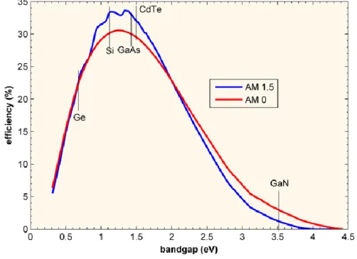
thermodynamic approach.11,14 Indeed, according to the Shockley Queisser detailed-balance model, the efficiency limit under non-concentrated sunlight condition is 31% (for a bandgap of 1.4 eV considering the AM 0 spectrum), and this efficiency limit under fully concentrated sunlight condition reaches 41% (for a bandgap of 1.1 eV). The SQ limit of a single junction is presented as a function of the bandgap in Figure 1-3
Figure 1-3 : Solar cell efficiency limit as a function of bandgap calculated using the Shockley-Queisser approach.13
As shown in Figure 1-4, in the SQ approach the solar cell can be modeled ideally using an electrical equivalent scheme composed by a continuous photo-generator in parallel with a diode (representing the pn junction). The continuous photo-generator electrical properties (Jsc,Voc) are strongly correlated with the material bandgap energy.
Independently of the SQ intrinsic limitation of solar cells, others sources of losses reduce their efficiency in realistic operating conditions. Those losses can have different origins such as reflections, Joule effect in metallic contact or the presence of structural defects in the semiconducting material. They can be modeled by adding series and shunt resistances (Rs, Rp) to the equivalent electrical scheme, which has a strong impact on the
Fill Factor. Figure 1-4 displays the corresponding simplified solar cell electric scheme.
In order to minimize those losses, different cells architecture can be used.15 Most of them use highly doped materials with wider bandgap than the absorber as back and front
Chapter 1: III-V MULTIJUNCTION SOLAR CELLS FOR CPV
8
surface field (BSF and FSF) to improve the efficiency by reducing series resistance and increasing shunt resistance. Also anti-reflective coatings are used to maximize the cell absorption of the solar spectrum. Moreover, a window layer can also be used to reduce the losses by carrier surface recombination. As an example Al is added to GaInP forming Al(Ga)InP in the emitter region. It helps to reduce the surface recombination velocity of carriers, that reduces the blue response of the cell, and hence its current. Also due to its large conduction band offset with GaInP, this material helps the electron collection in the cell. Al(Ga)InP is used in the BSF (Back Surface Field) region, as well, due to its large valence band-offset with GaInP which help the hole collection in the cell.
Figure 1-4 : Simplified solar cell electric scheme, including parasitic series and shunt resistances.
The lab efficiency records for single GaAs and Si solar cells, respectively 25,6 and 28%, are now close to the SQ limit considering each bandgap, making difficult and expensive any improvement of the efficiency of those single junction cells due to the SQ limit and almost unavoidable other losses, such as Joule losses in the metallic contacts.16 Those technologies can thus be considered as mature (i.e. with a very limited potential of improvement). To exceed this limit and reach higher efficiencies, advanced concepts have to be used.
High efficiency multijunction solar cells
1.2
To reduce the thermodynamic losses in solar cells, several concepts have been proposed such as intermediate band and hot carrier solar cells.17,18,19 The multijunction
9
solar cells (MJSC) is the most mature of those concepts. Indeed, the highest efficiencies ever registered for photovoltaic devices has been obtained using MJSC.20 It is a direct way of overcoming the fundamental limitations by using several absorbers with different band gaps, each one dedicated to harvest a part of the solar spectrum so that the losses due transparency and thermalization are both reduced.21 It is done by stacking the cells so that the top cell has the highest band gap, and harvests the highest energy photons, while the bottom cell has the smallest band gap, collecting the lowest energy photons. Among the different ways to connect electrically the cells, the most commonly used is the two-terminal stacking. In this case, each cell is series-connected by a tunnel junction, which should have a higher band gap than the cell below, be highly doped, and thin (few nanometers) to minimize its photons absorption and to allow an efficient carrier tunneling of the photogenerated carriers.22 Figure 1-5 shows a typical band diagram scheme of a single junction and a two-junction (“tandem”) solar cell.
Figure 1-5: Band diagram scheme of a single (up) and a tandem (down) solar cell.
In this configuration, cells are series-connected through the tunnel junction, thus the cell displaying the lowest current will limit the electric current through the overall MJSC. Therefore, to improve the efficiency, the bandgap of each cell has to be adjusted carefully to obtain a current matching between all the subcells. Figure 1-6 shows the maximum efficiency for a tandem solar cell under the AM1.5G spectrum as a function of its subcells bandgaps. In practice, such structure is realized by monolithical epitaxial growth of the different layers constituting the MJSC stack, using either metal-organic
Chapter 1: III-V MULTIJUNCTION SOLAR CELLS FOR CPV
10
vapor phase epitaxy (MOVPE) or molecular beam epitaxy (MBE), or/and using non-epitaxial methods such as wafer bonding, or non-epitaxial lift-off (ELO).23,24
Figure 1-6: Evolution of the overall efficiency of a tandem solar cell, as a function of top and bottom subcell bandgaps. The maximum efficiency for a tandem solar cell under the AM1.5G spectrum without concentration is 47 %. Using a 1.1 eV Si bottom cell, the maximum efficiency is obtained
for a top cell with a 1.7 eV bandgap.13
Most of the research progresses on MJSC have been realized on III-V material systems lattice matched with Ge, GaAs and InP substrates. This is due to their well-known excellent optical and electrical properties and their strong absorption due to their direct bandgap.25,26,27 Figure 1-7 displays the energy bandgap versus the lattice constant of the III-V and especially of dilute nitride compounds.13 The availability of ternary compounds such as GaInP lattice-matched to GaAs and quasi-lattice-matched with Ge, with adapted direct bandgap (see Figure 1-7), explains why this material system have been firstly studied for PV applications. The interest of lattice matched structure is to limit, or avoid, the misfit dislocations formation in epitaxial layer, that can reduce the solar cells performance. Different approaches such as wafer bonding, metamorphic and the use of dilute nitride materials, have managed to lower the overall cost by optimizing the bandgap combination and thus increase the efficiency through a better current matching. However, maintaining the GaAs, or Ge substrates to build the high efficiency III-V MJSC, undoubtedly incurs a substantial cost associated with such substrates.20 Nevertheless, a III-V/Si tandem solar cell on Si substrate promises high efficiency at
11
relatively low cost: a 1.7 eV junction on a 1.1 eV Si junction has the theoretical potential to achieve nearly the optimal efficiency for a tandem solar cell on silicon (cf Figure 1-6). Therefore a great research effort is now put on the integration of III-V PV on Si.
Figure 1-7: Energy bandgap as a function of the lattice constant of some of the group IV and group III-V semiconductors. 28
However, the use of Si substrates for high efficiency III-V MJSC has been impeded due to the large mismatch of both the lattice constants and the thermal expansion coefficients, between the substrate and the conventional cell alloys. These mismatches result in high densities of dislocations, leading to both low efficiencies and limited lifetime. The approach followed during my PhD work is based on the progresses made on the growth of GaP/Si and diluted nitride materials. Those progresses have given the hope of growing optically-active lattice-matched III-V materials on silicon using a GaPN based material.28,29,30 Indeed, by adding a small amount of arsenic and nitrogen in the GaP compound, a 1.7 eV pseudo-direct bandgap GaAsPN alloy, lattice-matched to Si can be grown. Considering the 1.12 eV energy bandgap of Si, this could open the route for a high efficiency lattice-matched solar cell on silicon. To understand the challenges and the interest of growing a lattice matched III-N-V/ Si tandem solar cell compared to the other approaches, a state of the art of the III-V MJSC for CPV is reported in the following.
Chapter 1: III-V MULTIJUNCTION SOLAR CELLS FOR CPV
12
Very high efficiency MJSC for terrestrial CPV and space applications
1.3
Lattice matched approach development
1.3.1
History and first breakthrough (a)
In the early eighties, numerous teams have focused their research effort on designing tandem cells devices with direct bandgap III-V compounds. To gain advantage of the low-cost Si substrate, most of those cells were first based on mechanical stacks of a high-bandgap top cell on a Si bottom cell or monolithic combinations of AlGaAs, GaAs, GaInAs or GaAsP on Si, without success, though those structures could theoretically reach efficiencies around 36–40%.5 In particular, in GaAs on GaInAs or GaAsP-based monolithic structures on Si, the interface defects due to the lattice mismatch between the III-V compounds with Si substrates were detrimental for the PV performances. Moreover, in the lattice-matched AlGaAs/GaAs system which could display a 36% theoretical efficiency, the strong effect of oxygen on AlGaAs even at low levels hampered its development at a commercial scale.31
In 1984, researchers at the National Renewable Energy Laboratory (NREL) proposed to work on the GaInP/GaAs system lattice-matched with a GaAs substrate, which has become the first commercially viable MJSC.32 It was made of a GaxIn1−xP top
cell (compound with a bandgap typically ranging from 1.8 to 1.9 eV) monolithically grown on a lattice-matched interconnecting tunnel junction and a 1.44 eV GaAs bottom cell. The Al-free and lattice-matched GaInP/GaAs approach proposed by NREL solves the issues previously encountered for a theoretical efficiency of 34%. Since 1990, efficiencies higher than 27% under AM1.5G have been obtained by modifying the top cell thickness to achieve current matching, for terrestrial application (under AM1.5G solar spectrum) as well as for space application (under AM0 solar spectrum and taking into account the particles irradiation).33,34,35,36,37,38 Then, the aerospace sector was rapidly attracted by these properties. Production of GaInP/GaAs solar cells (on Ge substrates) started in 1996, and the first GaInP/GaAs-powered satellite was launched in 1997. The record in efficiency, for terrestrial applications, is equal to 34.1% (under concentration of 467 suns, NREL).39
13
III-V triple-junction solar cells development (b)
Following the development of the mature GaInP/GaAs tandem cell, in 1997, researchers have proposed to add a third junction. Germanium was chosen as it was the perfect candidate due to its 0.67 eV narrow band gap and quasi-lattice-matching with GaAs. Introducing these third junction as the bottom one, the lattice matched (LM) GaInP/Ga(In)As/Ge stack displays [1.86eV/1.39eV/0.67eV] bandgaps combination, while highly current-mismatched due to an excess of photon absorption in the Ge bottom cell, this MJSC can theoretically reach a 38.6% efficiency without concentration.40 The small In amount (around 3%) in the GaAs was set for better lattice- and current-matching. However, even though Ga(In)As is closely lattice-matched with the Ge substrate, a high quality Ga(In)As/Ge heterointerface has been historically difficult to obtain, due to the mismatches in both the crystal structures and local chemistries. The polar (GaAs epilayer)/non-polar (Ge substrate) growth have first impeded the successful III-V/Ge monolithic integration, resulting in interface-related structural defects such as anti-phase domains (APD) and stacking faults (SF). While various “recipes” for the growth of GaAs on Ge(100) with good structural quality have been proposed, many present contradictory results.41,42,43,44,45,46 The cause of those different behaviors is not fully understood. It might be a consequence of differences in reactor design or material purity. It could also be connected to the quality of the Ge substrates preparation. Other research let think that it is related to the prenucleation conditions or the structure of the (100) Ge surface prior to the GaAs nucleation step. Nevertheless a few guidelines have been given to reduce the APD formation such as the cleanliness of the Ge substrate and its orientation (6° off along the [110] direction), to obtain bi-atomic step at the Ge surface, a full Ga monolayer coverage and the use of low-temperature migration enhanced epitaxy to promote a 2D growth.
Once the control of the heterointerface structural quality was achieved, the main problem was the control of group V or group III dopant diffusion into the Ge substrate. Due to the high temperatures (500-800°C) often needed for the heteroepitaxy, diffusion of both Group III and Group V atoms into the Ge substrate cannot be suppressed. Thus the challenge is to control this diffusion process while obtaining a defect-free GaAs heteroepitaxial layer with a suitable doping type and level.47,48 A full presentation of the best process is beyond the scope of this chapter, but here are
Chapter 1: III-V MULTIJUNCTION SOLAR CELLS FOR CPV
14
summarized the conclusions drawn in the literature (which we have been used in the framework of this thesis):40-45
(1)- Because of the thermal activation of the diffusion process, junctions are more stable at lower growth temperatures.
(2)- In the three-junction GaInP/Ga(In)As/Ge solar cells, the most important parameter of the Ge-cell is its output voltage, as the Ge cell is not the current-limiting junction. The Ge cell bias depends strongly on both the quality of the III–V/Ge interface and the Ge structural quality itself.
(3)- Due to its lower diffusion coefficient, P element is a better group V dopant for Ge than As.
Using such lattice-matched triple junction on Ge substrate, the last efficiency record using this approach was set by Spectrolab in 2010 at 41.6 % under 364 suns, close from its theoretical maximum (48% under 500 suns).49,50 Then, an improvement has been proposed using more optimal bandgap combinations than the [1.86eV/1.39eV/0.67eV] combination of the lattice-matched and current-mismatched GaInP/Ga(In)As/Ge structure. Nowadays, Lattice-Matched (LM) GaInP/Ga(In)As/Ge multijunction solar cells are standards for both space and terrestrial concentrator applications, with a lot of companies able to grow these cells such as Spectrolab and
Azurspace. The fabrication of these multijunctions is achieved by metal-organic
chemical vapor deposition (MOCVD) or molecular beam epitaxy (MBE).27,49,50
Metamorphic and non-epitaxial approaches
1.3.2
Lattice-mismatched approach (a)
The route to achieve higher efficiency is to approach the [1.75eV/1.18eV/0.70 eV] optimal bandgaps combination, for which the current-matching is achieved, by lowering the bandgaps of both the top and middle cells through an increasing of their indium content. However, this is obtained by paying the price of increasing the lattice-mismatch, and thus increasing the density of defects. The obtained structures are called LMM (Lattice-MisMatched). However, an efficiency of 41.1% at 454 suns has been
obtained in 2009 for a quasi-current-matched and lattice mismatched
Ga0.35In0.65P/Ga0.83In0.17As/Ge cell with bandgaps combination of [1.67eV/1.17eV/ 0.67
15
mismatch with the Ge substrate, meaning that they have been grown metamorphically.
An essential part for this metamorphic solar cell structure is the use of an optimized step-graded buffer structure made from a Ga1−yInyAs buffer layer between the Ge
subcell and the middle subcell. The step-graded buffer consisted of seven 200 nm thick GaInAs layers with stepwise increased indium content from 1% to 17%. The misfit dislocations generated in the buffer during the relaxation of the lattice stress were then well confined at the interfaces between the layers with different In content. Moreover, the bandgaps of the different layers inside the buffer layer are large so that the overall buffer is transparent to photons that have to be absorbed by the junction below. However, considering such a defects-containing structure, an important uncertainty remains about the evolution of the dislocations location with time, under solar cell operation. The tunnel diode consist of an intrinsically C-doped p-AlGaInAs layer and a Te-doped n-GaInP layer, and avoids the generation of dislocations by good lattice-matching with the surrounding layers. With this approach, obtaining the perfect current matching, to reach the theoretical efficiency, by decreasing the top two junction band gaps has been found to be very difficult because the cell performance is very sensitive to dislocations in the top GaInP junction.
Inverted metamorphic solar cells (b)
Thus a new concept has been proposed by the NREL to obtain a better current matching while minimizing the propagation of strain-induced defects through the device structure by growing the junctions in increasing order of lattice mismatch to the substrate in an inverted lattice-mismatched structure (IMM).24 The GaInP junction (1.86 eV) is grown first on a GaAs substrate, leading to a strained GaInP subcell while displaying a defect-free surface suitable for the growth of the slightly mismatched Ga0.96In0.04As middle junction (1.34 eV). Then, a highly mismatched Ga0.63In0.37As
junction (0.93 eV) is grown on top of the structure. Thus its strain-induced defects have limited effects on the other junctions. Since the growth of the subcells have implied an inversion in the bandgap order, this structure implies to remove the substrate to allow the light enter through the highest-bandgap subcell first. Therefore, prior to the GaAs substrate removal, the structure is first bonded to a low-cost host substrate (either Si or Glass, or a flexible substrate) for mechanical support. Again, step-graded buffer layers
Chapter 1: III-V MULTIJUNCTION SOLAR CELLS FOR CPV
16
are used between the mismatched junctions to relieve strain and confine dislocations away from the active regions of the junctions. The success of this approach is due to the tolerance of GaInAs to threading dislocations and to advances in the understanding of the growth of mismatched structures.52 This approach has led to a record of efficiency (April 2013) set by sharp with 44.4% efficiency under 302 suns.53 Nevertheless the effect of lattice mismatch on the reliability of those solar cells still needs to be evaluated.
Wafer bonded quadruple junction (c)
The theoretical optimum for a four-junction solar cell under AM1.5d spectral conditions is reached for a set of declining bandgap energies with 1.9, 1.4, 1.0, and 0.5 eV. In 2010, promising results were reported for inverted metamorphic devices reaching AM0 (space solar spectrum) one-sun efficiencies up to 33.6%.54 In this configuration, two lattice-mismatched GaInAs bottom junctions are combined with a GaInP/GaAs top tandem by using buffer layers to relax the crystal lattice. Dislocations cannot be completely avoided in this configuration, and this leads to constraints in device performance. Wafer bonding is another technology to combine lattice-mismatched materials without creating dislocations. Two crystal structures are brought closely together forming atomic bonds at the interface.55–57 This technology requires two epitaxial structures (and thus the use of two wafers) with low surface roughness and a specific surface preparation but offers the advantage of combining the best defect-free semiconductors in a multi-junction solar cell device. Wafer bonding has been used by several authors in the past.58–61 In 2014, for the first time, results of a four-junction device, have reach the level of the best triple-junction solar cells setting the efficiency world record with a peak efficiency of 44.7% at 297 suns concentration. This is
achieved by a Ga0.51In0.49P/GaAs top tandem bonded to a
Ga0.16In0.84As0.31P0.69/Ga0.47In0.53As bottom tandem solar cell (Figure 1). This
combination is close to the ideal bandgap combination for a four-junction device and allows one to reach excellent material quality for all junctions. Though important improvement have been made in term of wafer recycling. All bonding methods require two substrates, one for epitaxy and one for the layer transfer. This makes bonding
17
technics expensive, even if the LM substrate can be re-used multiple times, giving the need of a monolithical integration.
Dilute nitrides multi-junctions lattice-matched cells
1.3.3
In the case of the lattice matched Ga0.49In0.51P/Ga0.99In0.01As/Ge material
combination, the Ge bottom junction is known to generate a large excess current, which limits the device performance. To reach higher efficiency and maintain a lattice-matched architecture and avoid reliability issues, Solar Junction has resolved the long standing problem associated to dilute nitride III-V compounds and is now manufacturing a lattice-matched multijunction solar cell employing an 1 eV GaInNAsSb bottom subcell. This dilute nitride material system was first explored in 1994 in the active zone of laser diodes.62,63 Researchers were interested because it was observed that adding small amounts of nitrogen in III-V material such as GaAs leads to a decrease of the lattice constant along with a large decrease of the bandgap (called “giant bandgap bowing effect”).64
This specific behavior of the III-V dilute nitrides has been successfully described using the Band AntiCrossing model (BAC) and tight binding calculations (TBC).65,66,67,68 Electronegative N Atoms in GaAs and others III-V material tend to localize electrons with energy levels lying near the GaAs conduction band. The interaction between the N localized states and the GaAs Γ-extended states lead to the splitting of the conduction band into two subbands, thus lowering the bandgap of the material. By controlling the N and In compositions in GaAs, the GaInNAs alloy can be lattice-matched to GaAs or Ge, while having a bandgap ranging from 0.8 eV to 1.4 eV.69
Huge effort was made by many groups to grow GaInNAs single and multijunction solar cells. First, despite all these efforts, intrinsic defects or defects associated with N-induced localizes energy states, or H or C impurity species resulted in short minority carrier diffusion lengths, and therefore low quantum efficiency which resulted in low photocurrents and made it unsuitable as a third junction under the GaAs/InGaP subcells.70,71 Its development has been slowed by problems related to the MOCVD growth which is the standard technique used in industry to fabricate III-V solar cells. Nevertheless, dilute nitrides have been intensively studied using MBE,
Chapter 1: III-V MULTIJUNCTION SOLAR CELLS FOR CPV
18
which is the technology usually adopted for research of novel materials. Indeed, MBE has clear advantages over MOCVD for the dilute nitrides growth, as it reduces C-doping and hydrogen related complexes.69,72,73 Moreover, MBE allows a higher level of control of growth conditions as it enables relatively low growth temperatures which avoid phase separation and clustering effects, while the V/III ratio and the N amount available for nucleation can be controlled more precisely.
Nevertheless the growth window is narrow due to the large difference (more than 20%) between GaAs and GaN lattice constants and due to the huge difference between As and N atomic orbital energies, thus the growth of high structural quality GaNAs (and other dilute nitrides) is much more difficult than all classical III–V alloys
74–76,77,78
Moreover, it has been shown that dilute nitride materials are metastable; they have a propensity for separating rather than forming a homogeneous alloy. To incorporate enough nitrogen into the material, the growth has to be done at much lower temperature (in far-from-equilibrium conditions) than the growth of N-free alloys. This reduces the growth window for dilute nitrides with sufficient N concentration. This window becomes even narrower with increased indium content, due to a tendency to three dimensional (3D) growth with higher indium content. More recently, it was shown that the introduction of Sb into GaInNAs, expands the growth window towards two dimensional (2D) epitaxy while enabling the incorporation of higher In and N compositions. Under the optimum growth conditions, antimony is incorporated into the alloy at levels of 5–8%, well above the incorporation level of nitrogen, which is characteristic of reactive surfactants.79 One more central discovery was that the atomic N incorporation coefficient is constant. It means that the growth rate controls the N concentration when other growth parameters are constant.80,81 This gives to dilute nitride alloys major advantage in terms of yield and reproducibility as compared to any equivalent mixed column V, III–V alloy semiconductor system.82 Note that influence of other growth parameters on the N incorporation was also observed but the control of N concentration, and therefore the energy gap of GaInNAsSb, via group III rate seems to be the most reasonable from the practical/technological point of view.80,83,84
Non-radiative recombinations originating from point defects are known to be one of the biggest challenge for the dilute nitrides. They are mainly due to the low MBE growth temperature and the use of plasma source to produce reactive atomic nitrogen. In
19
general, the nature of N-related defects is not well understood.71,73,85–90 A portion of these defects can usually be removed by post growth annealing.91–96 Though, to realize high quality dilute nitrides the number of N-related defects in as-grown materials should be reduced, which can be done through a purposely designed N plasma source and optimal operation.97–101 For instance, low radiofrequency (RF) power and high flow produce the fewest ions impinging the surface, which minimize the point-defects generation, but also the N incorporation. Also it has been shown that using smaller, fewer holes in the aperture at the end of the plasma source decreased plasma damage and improved the stability of the plasma. 102 To eliminate the ions from the molecular beam, electrically biased metal plates can be mounted at the exit aperture of the nitrogen cell,77 which significantly improves the optical quality of GaInNAsSb. This finding has been one of the keys to the successful realization of high quality GaInNAsSb based solar cells. Indeed, this approach has led to an important record of efficiency in 2012, by Solar Junction, with 44 % efficiency under 967 suns using a GaInP/GaAs/GaInAsN(Sb) triple junction with the following bandgap combination: 1.89 / 1.41 / 1 eV.103 Another method has been developed to minimize the ion impact on the growth of dilute nitride materials such as the use of an ADDON valved rf plasma source that will be described more in details in the following chapter.
All these approaches to build high efficiency III-V MJSC are performed on expensive GaAs, or Ge, substrates. However, a III-V/Si tandem solar cell on Si substrate promises high efficiency at relatively low cost. Indeed, the PV market is still strongly dominated by Si single junction solar cells due to their lower production cost and the maturity of the Si industry. Thus in order to increase the market throughput of III-V MJSC researchers have proposed to use Si substrate instead of the III-V or Ge substrate which would allow a drastic cost reduction.
III-V Tandem solar cells on Si substrate
1.4
Motivation for the integration on Si
1.4.1
The use of Si as an alternative substrate material for III–V epitaxial solar cells in place of the common MJSC substrate materials (GaAs and Ge) would significantly reduce the cost of the PV energy. Indeed Si is at least 10 times cheaper than the
Chapter 1: III-V MULTIJUNCTION SOLAR CELLS FOR CPV
20
conventional MJSC substrate materials (1-3$ per square inch for Si wafers). Moreover, Si is also available in larger wafer sizes (300mm diameter in 2009 and 450 mm today) than typical 100–150 mm diameter of Ge or GaAs wafers. Since epitaxy and wafer-processing costs do not significantly change with wafer size, moving to a large area substrate (Si) would also decrease the solar cell fabrication cost. Another significant advantage of Si is that by shifting the III–V solar cell technology toward a Si platform, the mature Si technology can be accessed, enabling fast production ramp-up, high volume, and high market throughput. With expected solar conversion efficiencies of 30-40%, III-V MJSC on Si hold great promise to enable a large PV energy production, with significantly faster ramp-up and reduced capital investment than what could be expected for a technology requiring niche manufacturing, helping for a rapid and cheap energetic transition. Given the potential for cost reduction through both materials and manufacturing and the promise of III–V solar cell efficiencies nearing 40%, the case of III–V/Si is quite different from every other PV technology, already mature or being developed. Indeed, even for low-cost, lower-efficiency thin films technologies, or for Si and III–V cells produced in a niche environment, such rapid scaling is very difficult as significant market penetration requires both high efficiency and high throughput. Some silicon physical properties also present distinctive advantages over the conventional GaAs or Ge substrates for terrestrial CPV, space-based and photo-electro-catalysis PV systems. For water splitting system tandem structures might provide both adequate potential and efficient utilization of the solar spectrum. Compared to the more classical InP based system which needs bias to work, tandem structure could operate without any power input apart from the sun. Moreover due to the strong resistance of GaP to corrosion the Si/GaPN tandem structure could fulfill the requirement in term of stability needed for such application.104,105 For space-based PV systems, cell weight is a very important parameter due to launch payload weight and stowage limitations. Silicon has a mass density less than half that of the GaAs and Ge, meaning comparably sized solar cells on Si would weigh less than half of those based on the more conventional substrate materials. Furthermore, Si is also mechanically stronger, with fracture toughness twice that of GaAs and 50% greater than Ge, allowing for the use of thinner Si substrates and thus even greater reduction in system mass. Therefore, high-performance III–V/Si solar cells with conversion efficiencies equal to or greater than that achievable by
state-of-21
the-art III–V/Ge cells would yield an increase in specific power (W/kg) of at least 2×, but potentially upward of 4× (roughly 300 W/kg for GaInP / GaAs /Ge triple junction).106
For terrestrial applications, these particular properties are not very important, although reduced cell mass and increased mechanical strength are certainly beneficial, especially for use in such applications as large-area roof-top systems. However Si substrates possess a thermal conductivity approximately 2× higher than GaAs and Ge, in the case of terrestrial concentrator systems, where the mitigation of excess heat is paramount to high-performance operation, providing a more efficient transfer of heat out of the PV cell is another advantage.
As might be expected, given the numerous substantial advantages of III–V/Si hetero-integration for solar cells, several researches have been undertaken in pursuit of this goal. In the next sections we will discuss of the challenges and the results on III-V tandem solar cells grown Si.
Non-Epitaxial methods
1.4.2
The first methods for integration use non-epitaxial steps to transfer III–V materials to Si substrates such as wafer bonding.107,108,109 However for solar cells, where relatively large area is required, wafer bonding approaches suffer from mismatch issues due to difference in the coefficient of thermal expansion (CTE) between III–V compounds and Si, giving rise to cracking. Recently, III-V/Si integration has been achieved using the Smart Cut™ technology. In this technology, layers are removed from their epitaxial host substrate via a hydrogen ion implantation process that physically weakens a thin region of material beneath the epitaxial layer to accomplish layer separation by exfoliation. This technique yielded to crack-free GaInP/GaAs dual-junction solar cell structures bonded to Si, with promising preliminary results.110 Even if bonding processes are attractive for a variety of reasons, they generate a different set of potential limitations as compared with the monolithical heteroepitaxial integration. As for the case of the wafer bonded quadruple junction, bonding technics are expensive due to the use of two substrates.
Chapter 1: III-V MULTIJUNCTION SOLAR CELLS FOR CPV
22
Metamorphic approaches
1.4.3
Si/SiGe virtual substrate (a)
Knowing the numerous difficulties (i e materials mismatches) involved with III–V PV materials grown directly on Si substrates introduced earlier and explained in detail in the following section, a considerable amount of research has concentrated on splitting the problem into less complicated ones. This explains why another group-IV material, Ge, has received much attention. Indeed while the issues of the heterovalent interface still exist for GaAs grown on Ge (discussed in the next section), the problematic lattice constant mismatch and thermal expansion mismatch are almost suppressed. This makes the III–V/IV growth easier. Also, much attention has been paid on the Ge/Si system, where problems linked to the heterovalent interface are totally removed. In this system, only lattice constant and thermal expansion mismatches remain.111,112 In fact, Ge/Si (and the SiGe alloys) is the classical system in which much of the basic science regarding lattice mismatched heteroepitaxy of Face-Centered Cubic (FCC) materials has been studied.47 Two main methods for the Ge/Si integration exist: direct Ge growth on Si substrates, with adapted strategies for dislocation density reduction, and compositionally graded SiGe buffers.
To our knowledge, the only approach with PV commercial outlet uses compositionally graded SiGe alloy buffers. As discussed previously for the case of III– V metamorphic cells, the objective of these methods is to relief the misfit in a controlled and efficient way. Until now, step grades have found more success. After the important work of the early 1990s on the realization of relaxed Si1−xGex layers on Si substrates
rapid progress were made in the development of a step-graded SiGe buffer technology to yield low defect density Ge virtual substrates.47,113 This original buffer design spreads the lattice mismatch strain over a thickness of about 10 μm and uses a midgrowth (Si0.5Ge0.5) chemical–mechanical polishing to reduce the deep crosshatch-induced
surface roughness (a result of dislocation glide at misfit interfaces). Moreover it takes into account the difference in thermal expansion between the various alloy compositions and final Ge layer, and yields to a final Threading Dislocation Density (TDD) of 1 × 106 cm−2, a value allowing the realization of efficient solar cells. Numerous researchers have since further refined the SiGe buffer process, reporting final Ge layer TDDs in the
23
105 cm−2 range reinforcing SiGe as the current state-of-the-art path for highly mismatched III–V compound integration on Si substrates.114
GaInP/GaAs dual junction on Si substrate (b)
With all the improvement recently made in the growth of SiGe/Si virtual substrate, efforts for growing a GaInP/ GaAs dual junction are increasing but are currently at an early stage. Nevertheless already interesting performances have been reported. It was demonstrated that p/n GaAs solar cells integrated on Si can reach very similar performances to homoepitaxial p/n GaAs solar cells.115 The main effect of the low concentration of residual dislocations on minority carrier transport in GaAs/Si solar cells is the large disparity of electrons and holes mobility which affects the choice of the device polarity. As in the case of the single-junction cells, the transmission electron microscopy (TEM) reveals very high-quality material through the whole structure, and includes not only GaAs and GaInP cells, but a thin GaAs p+/n+ tunnel junction that provides a low-resistance connection between the series-connected sub-cells.116 With this architecture, a Voc value of 2.21 V under AM0 illumination is reported. Assuming
that the GaAs sub-cell provides Voc∼0.98 V from the single-junction experiments, the
GaInP is providing Voc ∼1.23 V. Note that this is an underestimated value of Voc for the
GaInP cell since the spectrum incident on GaAs is now at a much lower incident flux due to the presence of the GaInP top cell, which in reality will slightly reduce the GaAs Voc value. The overall high value for the Voc of the dual-junction cell indicates that very
good material quality has been maintained throughout the dual-junction structure. This was confirmed by the reasonable match with the Voc value obtained for identical dual
junctions grown on GaAs and processed side-by-side, which produced 2.34 V under AM0 conditions. The overall efficiency of the dual-junction cell on Si was 16.8% under AM1.5G illumination. The performance is limited by several external factors that reduce the current output by several mA.cm−2, including a large 10% grid shading, the use of a GaAs tunnel junction as opposed to a wider bandgap tunnel junction, and a relatively poor antireflection coating. Correcting such issues, this very promising technology should realize 1-sun efficiencies well in excess of 20% on Si for only two active junctions. Future works can lead to the addition of a third Ge sub-cell using the
Chapter 1: III-V MULTIJUNCTION SOLAR CELLS FOR CPV
24
top layer of the SiGe graded buffer, following the example of GaInP/GaAs/Ge triple junctions that are state-of-the-art but are grown on high-cost Ge substrates.
GaAsP/SiGe tandem solar cells on Si substrate (c)
Another very interesting approach has been proposed by 4Power.117,118 They have demonstrated a monolithically integrated solar panel on Si that allows scaling of cell output voltage on the wafer level, with a GaAsP/SiGe dual junction solar cell on Si. This provides ideal bandgaps to reach the highest efficiency for solar spectra between AM0 and AM1.5. Combined with CMOS-based active power management the solar panel on wafer (SPOW) design enables maximum output power and ideally managed power profiles under non-ideal, and time-varying illumination conditions. This results in improved reliability, lower system cost, and higher specific power over conventional III-V PV array technology. The structure is grown in a IV/III-V MOCVD growth cluster. The threading dislocation density of the SiGe buffer layer is very low (in the range of 8.105 cm-²). The III-V layer is free from APD. The Ge diffusion in the III-V layer is low in the range of 1016 cm-3. The structure is grown at high growth rate enabling the solar cell production in less than an hour. The last reported efficiency of these cells was around 20% but large improvements are expected as the tunnel junction was not optimized. From 4Power point of view, reaching a 30% efficiency is a realistic objective for this cell configuration. Tough those performances would be fantastic and would totally change the energy market, due to the lack of experience on the reliability of metamorphic solar cells, industrials are still afraid of investing in this solution which gives room for research on a lattice matched approach that would combine: high efficiency, low cost and high reliability.
The Pseudomorphic approach and its challenges
1.4.4
The lattice matched approach using dilute nitride material, which is the main research topic of this thesis, may offer several advantages. Though a number of material issues, explained in detail below remain to be solved, this architecture would combine: high efficiency, low cost and high reliability, making it potentially very interesting for a large scale development of the PV energy. In pursuit of this goal, researchers at NREL have proposed in 2002 to work on the GaPN dilute nitride material system, as this
25
material can be lattice matched with Si and have a strong absorption around 1.9 - 2 eV making it suitable as the top junction absorber.28 Moreover by adding Al, As, In or Sb, and controlling the N content in the layer one can theoretically form lattice-matched alloys having bandgap around 1.7 eV which could allow a better current matching with the Si cell. Using this approach they have demonstrated a tandem solar cell with a 5.2 % efficiency, using a MOCVD-grown 1.7 - 1.8 eV direct bandgap GaAsPN dilute-nitride (p-i-n top junction lattice-matched with the Si), deposited on a 1.1 eV diffused Si bottom cell.119 However, though the dilute III-V nitride addresses the lattice mismatch issue, the efficiency achieved was low due to the low-structural-quality of the III-V/Si interface, GaAsPN top junction and the poor quality of the tunnel junction and contacts.119 In the following I present in detail the main challenges related to the pseudomorphic approach to understand the interest of this thesis work.
GaP/Si virtual substrate (a)
As was discussed previously, there are a number of important materials incompatibilities between group-III–V and group-IV semiconductors. Strategies necessary for the successful integration of GaP materials on Si substrate were pull out from the research done on GaAs/Ge, including necessary substrate orientation and preparation, and the proper control of GaP nucleation on the Si surface.45,120–125 Unfortunately due to the strength of the Si-N bonds and amorphization of the III-V/Si
interface, GaPN can’t be grown directly on Si and a thin GaP layer has to be grown.119
In the following I present in detail the main challenges related to the growth of III-V compound on Si substrate, and the analogies and differences between GaAs/Ge and GaP/Si integration to understand the strategies that have paved the way for the successful integration of III-V semiconductors on group-IV substrate.
i. Materials challenges for III-V/Si monolithic integration
The unifying goal of all monolithic approaches is the control of defects related to the multiple materials properties incompatibilities, which can be detrimental to solar cell performance. In the following section we will discuss about the material incompatibilities and the challenge of the metamorphic and the pseudomorphic approaches
Chapter 1: III-V MULTIJUNCTION SOLAR CELLS FOR CPV
26
Most of the problems were materials-related issues of the III–V/Si heteroepitaxial interface, due to several materials properties differences such as: lattice constant, thermal expansion and heterovalent interface. Indeed GaP is polar material with a zinc blend crystalline structure having a 5.450 Å lattice constant while Si is non-polar with a diamond-like crystalline structure having a 5.431 Å. A number of crystalline defects may result, due to the mismatch of crystal symmetries between the two types of materials. 118,119,120,124,125–128,129,130,131,134,135 These defects can be divided into two classes. On one hand, extended planar defects such as: stacking faults and microtwins (MTs) are due to nonoptimal III–V nucleation morphology and growth of polar material on non-polar one.
On the other hand anti-phase domains (APDs) and anti-phase boundaries (APBs) are due to the heterovalent interface, (growth of polar III-V materials on nonpolar Si substrates). Both types of interface defects are electrically active, potentially detrimental to any integrated devices. They are especially problematic for minority carrier devices, such as solar cells, as they can serve as highly efficient recombination centers, as well as current shunt paths.136,137
Given the many difficulties and potential sources of detrimental defects in the monolithic integration of high-performance III–V materials on Si substrates, it is not surprising that it is still a highly active area of research, even after over 30 years of constant attention, but not yet a mainstream technology. However, much progresses have been made over the years, bringing the goal ever closer to the full realization of optoelectronic device on Si. In the last decade, the development of a methodology for epitaxial integration of GaAs on Ge(100) substrates has paved the way for a III–V on Si technology through the use of SiGe graded buffers. And recent works have even helped break through the barriers that had been preventing a realization of direct III–V/Si integration, demonstrating high-quality devices, and defect-mitigated epitaxy of GaP on Si(100).138,139,140
We discuss in the next sections of this chapter some of the approaches undertaken to monolithically integrate III–V semiconductors on Si substrate to produce high-performance PV materials.