HAL Id: hal-02413064
https://hal.archives-ouvertes.fr/hal-02413064
Submitted on 14 Dec 2020
HAL is a multi-disciplinary open access
archive for the deposit and dissemination of
sci-entific research documents, whether they are
pub-lished or not. The documents may come from
teaching and research institutions in France or
abroad, or from public or private research centers.
L’archive ouverte pluridisciplinaire HAL, est
destinée au dépôt et à la diffusion de documents
scientifiques de niveau recherche, publiés ou non,
émanant des établissements d’enseignement et de
recherche français ou étrangers, des laboratoires
publics ou privés.
quantum nanophotonics
Tian Zhong, Philippe Goldner
To cite this version:
Tian Zhong, Philippe Goldner. Emerging rare-earth doped material platforms for quantum
nanopho-tonics. Nanophotonics, Walter de Gruyter, 2019, 8 (11), pp.2003-2015. �10.1515/nanoph-2019-0185�.
�hal-02413064�
Tian Zhong1 and Philippe Goldner2
1Pritzker School of Molecular Engineering, University of Chicago, Chicago, IL 60637, USA 2
Institut de Recherche de Chimie Paris, PSL Research University, Chimie ParisTech, CNRS, 11 rue Pierre et Marie Curie, 75005 Paris, France
(Dated: June 19, 2019)
Rare-earth dopants are arguably one of the most studied optical impurities in solids, with applica-tions spanning from laser optoelectronics, biosensing, lighting to displays. Nevertheless harnessing rare-earth dopants’ extraordinary coherence properties for quantum information technologies is a relatively new endeavor, and has been rapidly advancing in recent years. Leveraging the state-of-the-art photonic technologies, on-chip rare-estate-of-the-arth quantum devices functioning as quantum memories, single photon sources and transducers have emerged, often with performances unrivaled by other solid-state quantum technologies. These existing quantum devices, however, nearly exclusively rely on macroscopic bulk materials as substrates, which fundamentally limits the future scalability and potential functionalities of such quantum systems. Thus the development of new platforms beyond single crystal bulk materials has become a priority. In this review article, we summarize the latest progress towards nanoscale, low-dimensional rare-earth doped materials for enabling next genera-tion rare-earth quantum devices. Different platforms with variety of synthesis methods are surveyed. Their key metrics measured to date are presented and compared. Special attention is placed on the connection between the topology of each platform to its target applications. Lastly, an outlook for near term prospects of these platforms are given, with a hope to spur broader interests in rare-earth doped materials as a promising candidate for quantum information technologies.
PACS numbers:
INTRODUCTION
Solid-state quantum nanophotonics has emerged as one of the most active fields in quantum engineering. In par-ticular, optically active atomic or atom-like defects in solids that simultaneously possess long-lived spin coher-ence and stable optical transitions play key roles in the development of quantum networks, quantum sensing and quantum information processing. Among numerous can-didates, rare-earth doped materials have attracted signif-icant interests in recent years, and is rapidly advancing. The emergent field of rare-earth nanophotonics inherits the rich history of rare-earth spectroscopy, and leverages the cutting-edge nanophotonic technologies to enable a new class of devices that are highly coherent, efficient and scalable. At the heart of this development is the funda-mental science and engineering of rare-earth doped mate-rials with wide variety of chemical compositions, physical behaviors, topologies and synthesis methods. The rich library of material properties offers nearly unlimited op-portunities for quantum device engineering. At the same time, crucial device metrics also dictate the best com-bination of material topologies and growth technique to achieve those specifications.
Only recently the connection between material growths and quantum device engineering has been made, and the importance of material design and synthesis has been rec-ognized. After decades of arduous efforts in perfecting bulk, single crystal hosts, newer platforms based on rare-earth doped nanocrystals, polycrystalline ceramics and films tailored for quantum technologies have been
gain-ing momentum and begin to reap promisgain-ing results. In this article, we summarize some of the most recent de-velopments in emerging material platforms beyond bulk crystals for building next generation rare-earth quantum photonic devices. We attempt to establish a common ground for material chemists, spectroscopists and device engineers in this field by highlightening the relationship between material metrics and device functionalities. The hope is to spur further research in fundamental material science to understand, control and design better materi-als to meet the needs of fast-growing rare-earth quantum technologies. It should be pointed out that we do not in-tend to give a thorough review on rare-earth doped bulk crystals, nor the spectroscopic techniques used to char-acterize them. A number of works on those topics are already available to the interested reader [1–5].
This article is organized as follows: Section 2 gives a review of rare-earth quantum photonic device developed to date and highlight the trend in underlying material platforms. Section 3 surveys in more details the progress in several emerging material platforms. In Section 4, we give an outlook for future material development and elab-orate several key metrics need to be accomplished in or-der to push forward the field of rare-earth nanophotonics.
RARE-EARTH QUANTUM PHOTONIC MATERIALS AND DEVICES
Rare-earth elements include lanthanides, scandium and yttrium. They are common dopants in host crystals
such as yttrium aluminum garnet (Y3Al5O12 or YAG),
Y2SiO5 (YSO), Y2O3, or YVO4 (YVO). The 4f shell of
rare-earth ions in crystals is partially occupied and is shielded from the interaction with the crystalline envi-ronment by 5s and 5p outer shells. The 4f electrons are highly localized and the 4f-4f intra-shell transitions are parity forbidden in free space, but become weakly al-lowed in the presence of crystal field, which result in sharp optical transitions with high quantum efficiency. Sharp optical transitions (equivalent quality factor over 1011) at cryogenic temperatures are correlated with long
optical T1lifetimes (hundreds of µs to ms) but also weak
oscillator strengths. Electronic Zeeman and hyperfine transitions in the radio-frequency or microwave regimes are abundant. When doped into host with small nuclear magnetic moments such as YSO, record long spin co-herence times 6 hours in Eu:YSO [6] and 1.3 seconds in Er:YSO [7] have been achieved. Such long coher-ence times combined with a rich selection of spin levels (both electronic and nuclear) and optical addressability make rare-earth ions attractive candidates for qubits as a building block in quantum information science. Further-more, optical transitions exhibit inhomogeneous broad-enings that are typically 105−6 times the homogeneous
linewidths, indicating an excellent prospect for dense spectral multiplexing of qubits or memories to enable large data processing and storage bandwidths [8, 9].
One of the most successful application of rare-earth doped crystals in quantum technology is optical quan-tum memories. These memories which faithfully store a qubit encoded on a single photon have performances un-matched by any other solid-state system. For reviews on rare-earth quantum memories, readers are referred to ref. [10, 11]. Landmark ensemble experiments in-clude storage of light up to a minute using electromag-netically induced transparency (EIT) in praseodymium doped yttrium orthosilicate (Pr3+:YSO) [12, 13],
quan-tum storage of photonic entanglement in neodymium (Nd) doped YSO (Nd3+:YSO) [14, 15] and
thulium-doped lithium niobate waveguides [16], optical memory at the single photon level in Nd doped yttrium ortho-vanadate (Nd:YVO) [17–19] and quantum level spin stor-age in Eu3+:YSO [20], conditional phase shifts between
two ensembles of europium (Eu) in YSO [21], up to 69% efficient quantum memory for light in Pr3+:YSO [22– 24], and a quantum optical connection between a cold atomic gas and Pr3+in YSO [25]. These ensemble-based memories provide natural interfaces between optical pho-tons and spins at radio-frequency or microwave regimes, which can also be harnessed to realize quantum trans-ducers interconnecting distant superconducting quantum circuits. Hybrid quantum systems based on rare-earth ensembles see the opportunities of microwave quantum storage [26] and microwave-to-optical conversion [27, 28]. To date, high cooperativity coupling of rare-earth spins to a superconducting resonator has been demonstrated
[29, 30]. Unit efficiency microwave to optical conversion via magneto-optic coupling has been proposed [28], and its experimental implementation is being pursued [31– 33].
Ultimately, the most powerful rare-earth quantum technologies will be devices operating on invidividual ions [34]. To that end, optical addressing of single ions is coming into focus of this research. Such a task, how-ever, is not easy. The progress has been hindered by long optical lifetimes of rare-earth ions and resultant faint photoluminescence. So far, only a few experiments have succeeded in isolating individual praseodymium [35–37], cerium [38–40], neodymium [41] and erbium [42, 43] ions. It is worth noting that majority of these experiments were not probing ions via their highly coherent but weak 4f-4f optical transitions. Taking Pr and Ce as examples, bright 4f-5d transitions from high lying electronic levels were exploited to enhance the detection sensitivity of in-dividual ions. To directly access the 4f-4f transitions of single ions, the emission rates of individual emitter need to be enhanced. Recent works by [41, 43] have been suc-cessful in that by coupling ions to nanophotonic cavities with sub-wavelength scale dimensions (more discussions on cavities in the next paragraph). Both experiments achieved Purcell enhancement of ions’ emission on the order of hundreds, allowing direct optical detection of individual ions with sufficient signal-noise performance using state-of-the-art superconducting nanowire detector technology. These results point at a viable approach to efficiently detect and coherently control individual ions in an on-chip nanophotonic platform.
The weak oscillator strengths of raearth emitters re-quire significant enhancement of their atomic absorption cross-sections in order to strongly interact with light at the quantum level. One effective way to achieve such enhancement is to modify the local photonic density of states using nanophotonic structures including uides and cavities. Rare-earth doped photonic waveg-uides have been realized by ion-indiffusion in Tm or Er doped LiNbO3 [16, 44, 45], laser written channels
in Pr:YSO crystals [46], and high-index membranes de-posited or transferred on top of doped oxide substrates [43, 47–49]. These waveguides provide transverse con-finement of the optical field interacting with dopants, thus enhancing the coupling strengths. In the cases of ion-indiffused and laser written devices, the rare-earth emitters align with the peak field intensity in the waveg-uide. Whereas in systems based on high-index materials placed on top of doped crystals, the optical field evanes-cently couples to the dopants near the material interfaces. All of these designs have demonstrated enhanced light-matter interactions, and preserved optical coherence of the dopants comparable to bulk crystal hosts. The long coherence despite the fabrication processes highlights the remarkable robustness of rare-earth dopant as a quan-tum resource. The waveguide scheme has also been
ex-tended to cavities by forming a micro-ring [48, 49] or patterning photonic crystal lattices [43] along the waveg-uide. For cavity-based system, an important figure of merit is the Q/V ratio where Q is the quality factor and V is the normalized mode volume of the cavity in a unit of (λ/n)3 [50]. Focused ion beam-milled photonic
crystal nanobeam resonator achieving Q/V on the order of 104 have been fabricated [51, 52], which enabled first
nanophotonic quantum memories [19, 53] based on meso-scopic ensemble of dopants and coherent optical address-ing of individual ions. The photonic crystal cavities were proven effective to strongly enhance the spontaneous emission rate of rare-earth ions via the Purcell effect [41, 43]. When the enhancement is sufficient large com-pared to other optical dephasing processes of the emitter, radiatively-limited single photon emission from individ-ual ions becomes feasible and has been demonstrated re-cently [41]. Besides waveguides and cavities, other tech-niques for controlling the rare-earth emission rates were also proposed. One example is a hybrid scheme in which the rare-earths are coupled to highly optically absorb-ing materials such as graphene via near field interactions [54].
YAG film
Si substrate 1 μm
Y2SiO5 bulk crystal
bulk nanocrystals thin films
100 nm
FIG. 1: Evolving material platforms for rare-earth quantum devices from macroscopic bulk crystals (Reprinted from [10]) to low-dimensional materials including doped nanocrystals (Reprinted from [55]) and sub-micron thick films.
RECENT PROGRESS TOWARDS LOW-DIMENSIONAL RARE-EARTH DOPED
MATERIALS
Majority of rare-earth quantum photonic devices demonstrated to date have been based on bulk, single crystal doped materials. These macroscopic bulk ma-trices, while having superb crystalline qualities, remains difficult to grow and lacks the essential prospect for scal-able fabrication desired by future quantum technologies. Perhaps most scalable platforms for on-chip device inte-gration are submicron thick membranes, on which large arrays of devices can be lithographically patterned and etched. High quality thin membranes of rare-earth doped materials have not been commonly available due to their
complicated chemical compositions and difficult growth processes. Most promising synthesis methods so far are atomic layer deposition and molecular beam epitaxy, the latest development of which will be discussed in the next section. Another class of doped materials promising for nanophotonic applications is nanocrystal and polycrys-talline ceramics. These powder form materials, once believed less promising for quantum applications, have gain significant tractions due to recent reports of long coherence even though the size of these nanocrystals is as small as 60nm [56]. The rare-earth doped nanocrys-tals are promising systems for single ion detection and control since they minimize background signal and can allow for higher Rabi frequencies in microscopy setups [36, 56, 57]. They can also be inserted into high qual-ity factor micro-cavities to enhance light-atom interac-tions, increasing emission rates through the Purcell ef-fect and collection efficiencies [58]. Perhaps the biggest advantage of nanocrystals is their relatively easy synthe-sis methods. Compared to single crystal bulk materials or epitaxial films, many nanocrystals can be grown with commercially available raw materials and in-house pro-cessing capabilities. Once this technology is matured to show consistent, robust coherence, the rare-earth doped nanocrystals can find widespread adoption as practical quantum technologies for sensing and communications.
Low dimensional host matrix
Nanocrystals and polycrystalline ceramic materials A first approach to obtain these materials is to use chemical methods, the so-called bottom-up strategy. This has been first used to produce Eu3+:Y
2O3micro-size
particles with 60 nm crystalline domains by a solvother-mal method [56, 59]. These particles, as most of those studied so far by high-resolution and coherent spec-troscopy, are polycrystalline, i.e. each particle is made of several crystallites. Optical properties were determined on samples in the form of a powder. Photon echoes, well known for providing an accurate measurement of homo-geneous linewidths in transparent materials [60, 61], can also be observed in powders that strongly scatter light as first demonstrated by Beaudoux et al. [62] and recently theoretically analyzed [63]. Application of this technique to the above particles led to a homogeneous linewidth for Eu3+ 7F
0 →5D0 transition at 581 nm of 86 kHz at
1.3 K [56]. This was about one to two orders of mag-nitude lower than previous results obtained on Eu:Y2O3
nanocrystals ([64]). It is however much larger than val-ues obtained in the best single crystals (300 Hz [65]) or transparent ceramics (3.5 kHz) [66], although it shoud be noted that considerable dispersion of linewidths is found in single crystals grown by different methods [67].
very detrimental to cavities quality factor, and should be as small as possible. The particle diameter d is a major factor to consider since the scattering cross-section varies as d6[58]. Moreover, to be able to use isolated particles,
aggregation should be avoided. This was made possible using homogeneous precipitation, a technique that lead to low particle size dispersion and spherical shapes [68]. To obtain Y2O3cubic phase, high temperature annealing
of the precursor hydrocarbonates particles is required. It was shown that treatment at 1200◦C reduced inhomoge-neous linewidths down to ≈10 GHz for 0.5% Eu3+
dop-ing, a value comparable to bulk ones [69]. This was ob-served for particle and crystallite sizes in the ranges 150-540 nm and 90-120 nm respectively, suggesting that the decrease in linewidths was due to a decrease in defects, such as oxygen vacancies, in the volume of the nanocrys-tals. On particles of 400 nm diameter (130 nm crystallite diameter), an extensive study of homogeneous linewidths Γh as a function of temperature, magnetic field and time
was performed by 2 and 3-pulse photon echoes and spec-tral holeburning [70]. A surprising result was that mag-netic fields up to 2.5 T had no effect on Γh, suggesting
that dephasing from magnetic defects or impurities was not the main contribution to Γh. Indeed, it was
con-cluded that for temperatures < 12 K, Γhwas due to
inter-actions with two-level systems (TLS) and a temperature independent dephasing. While TLS effect has been previ-ously identified in Y2O3 bulk crystals and nanoparticles
[56, 67], it was not the case for the latter process. Based on a simple model, it was suggested that it can be due to electric field noise created by surface charges, a mech-anism already observed in NV− centers in diamond for example [71]. Importantly, no sign of interaction between Eu3+ and a modified phonon density of states, related to
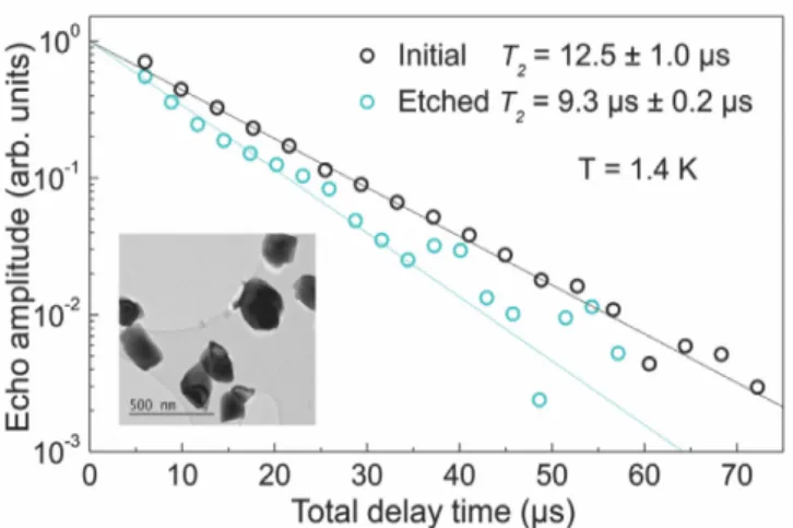
the crystallite sizes [64], was observed. This indicates that there is no intrinsic size-related contribution, which would be very difficult to overcome, to the homogeneous linewidth of the studied particles. The narrowest homo-geneous linewidths reported were 45 kHz at 1.3 K with a broadening of ≈100 kHz over 1s [70]. Narrow linewidths were also demonstrated in smaller particles. Because of the required high temperature annealing that promote sintering, it can be challenging to directly obtain small particles that stay non-aggregated. An alternative ap-proach was proposed in which large particles are reduced in size by wet chemical etching in a weak acid. Start-ing from dispersed and well crystallized particles of 450 nm diameter, particles down to 150 nm were obtained showing homogeneous linewidths of 34 kHz at 1.4 K, the smallest value reported so far for a nano-material [72]. The limited broadening induced by etching (≈ 10 kHz), while the particle size is reduced by 65% but the crys-tallite size remains unchanged, suggests that the latter is the relevant parameter for dephasing processes (Fig. 2). This was further supported by showing that etching pro-ceeds by opening grain boundaries between crystallites
FIG. 2: Optical echo decays in Eu3+:Y2O3 nanoparticles
be-fore and after chemical etching. Despite the size reduction from 450 nm to 150 nm, only limited broadening (≈ 10 kHz) is observed. Inset: 200 nm etched particles. Reproduced from Ref. [72] with permission from the Royal Society of Chem-istry.
in the particles. Single crystalline particles can therefore be produced, which may be useful when, for instance, a magnetic field should be applied in a specific direction or well defined Rabi frequencies are needed.
To assert the potential of rare-earth doped nanopar-ticles as quantum memories or processors, it is neces-sary to measure spin coherence lifetimes T2 since qubits
are usually defined within the energy level structure of ground state spins [73]. This was performed on 400 nm Eu3+:Y2O3 particles using an all-optical technique for
spin coherence manipulation and spin echo detection [74– 76]. Powders cooled to 5 K showed nuclear spin echo signals for 151Eu3+ with signal to noise ratio of about
10, proving that the technique actually works in a scat-tering medium, and sufficient for T2 measurements [77].
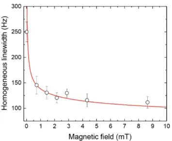
Spin coherence lifetimes of 1.3 ms were recorded, increas-ing to about 3 ms under a 9 mT magnetic field (Fig. 3). These values, one order of magnitude lower than in trans-parent ceramics [78] but still the longest reported for any nanoparticle with optically addressable spins, pro-vide valuable insight into dephasing mechanisms. First, the strong dependance of T2for very weak magnetic field
suggests that the main dephasing is due to magnetic dipole-dipole interaction with electron spins carried by defects or impurities. Indeed, when the Zeeman inter-actions become larger than the dipole-dipole interaction, the effect of the latter is reduced. This magnetic noise also affect the optical transition, which can be expected to broaden to a similar level than the spin transition, i.e. ≈250 Hz, based on the excited and ground state gyro-magnetic ratios in other hosts [79–81]. This is much too small to account for the optical linewidth of 45 kHz and supports the hypothesis of electric field perturbations as the main optical dephasing process. This is also in
agree-FIG. 3: Nuclear spin homogeneous linewidth of
151
Eu3+:Y2O3 (±1/2 → ±3/2 ground state transition)
in Y2O3 nanoparticles as a function of external magnetic
field. Reproduced from Ref. [77], CC-BY-4.0.
ment with Stark coefficient of the optical transition [82] being 4 to 5 orders of magnitude larger than the spin one [83]. Coherent spin control was further demonstrated by an all-optical dynamical decoupling (DD) technique that resulted in T2 up to 8 ms, limited by disorder and light
scattering in the powders that prevent pulses with accu-rate area to be applied [77]. This highlights the inter-est of using single particles with single crystalline struc-ture for optimal decoherence control. It was also shown that spin state phase is well preserved in echo and DD sequences, which is a requirement for quantum storage. Apart from experiment on powders, spectroscopy of sin-gle Eu3+:Y
2O3 nanoparticles has been studied using a
fiber micro-cavity [58]. In this setup, the particles are placed on a flat mirror which faces a concave profile laser-machined in an optical fiber. It was found that Eu3+ in
90 nm particles had inhomogeneous linewidths identical to what had been measured on powders, and that the cavity allowed detecting about 10 ions taking advantage of the Purcell effect.
Similar results have also been reported in Pr3+:Y2O3
nanoparticles [D. Serrano et al., in preparation], obtained by homogeneous precipitation, for optical and spin tran-sitions. Compared to Eu3+, Pr3+has generally stronger optical transitions and more favorable branching ratios that could be beneficial for coupling to a cavity. Hyper-fine splittings are however smaller [2], which limits the minimal pulse duration that can be applied to a specific transition between hyperfine levels and therefore oper-ation fidelity. Homogeneous linewidths of between 100 and 300 kHz were observed for the3H
4→1D2transition
at 619 nm and particles between 400 and 150 nm (crys-tallite size 120 and 80 nm). Interestingly, spin coherence
lifetimes reached nearly 1 ms, longer than reported so far in bulk Pr3+ doped crystals, like YSO [84, 85]. This could be explained by lower gyromagnetic ratios for Pr3+ in Y2O3 according to calculations based on crystal field
modeling of electronic levels [86, 87].
Pioneering experiments on high resolution spec-troscopy of rare earth doped nanomaterials used a top-down approach, laser ablation, to produce Y2O3
nano-crystals with a monoclinic phase [64, 88]. Spectral hole burning was used to probe Eu3+ homogeneous
linewidths, which were found in the several MHz range for crystals of 10s of nm, likely to be highly agglomerated. Interactions with modified phonon density of states were proposed to explain the broadening.
Other top-down approaches have also been investi-gated, in which a single crystal is ground to nanopar-ticles. In Pr3+:YSO, optical homogeneous linewidths of a few MHz for single ions were reported for particles be-tween 100s of nm and a few microns, as well as spectral diffusion of 10 MHz over minutes for the larger parti-cles [36, 89]. Strain induced by grinding and associated TLS could be the source of this significant broadening compared to the 80 kHz linewidth in the bulk crystal. Such mechanisms were also put forward in studies on Tm3+doped crystals ground to micron size powders and
probed by spectral hole burning [90]. The main effect of strain was observed on spectral hole lifetimes that strongly shortened under milling (several hours down to 10s of minutes) and could be partially recovered with high-temperature annealing. Homogeneous linewidths, that can be estimated from hole widths, followed the same trends although the already broad values of several MHz for bulk crystals do not allow studying very narrow linewidths. Milled, micron-size powders of Er3+:LiNbO
3
were also studied by spectral hole burning and photon echoes, and showed that even low energy milling impacts kHz range homogeneous linewidths [91]. For powders with 1-100 µm crystals, annealing was able to recover close to bulk properties.
Another class of polycrystalline materials are trans-parent ceramics, which are usually obtained by sintering cubic phase nanoparticles under high temperature and high isostatic pressure (HIP). This results in the growth of micron size crystals with random orientation and a strong decrease of the material porosity, ultimately lead-ing to negligible scatterlead-ing losses [92]. Thanks to their high flexibility in composition, shape, and ability to build composite materials, transparent ceramics are thus an al-ternative to single crystals in a variety of photonic appli-cations like lasers or scintillators, and could also allow obtaining new high performance materials in quantum technologies [93–95]. Eu3+ in Y
2O3 transparent ceramic
properties have been investigated in details, as a func-tion of doping concentrafunc-tion, post-synthesis treatment and co-doping with sintering aids. Optical transition in-homogeneous linewidths down to 9 GHz were observed
for 1000 ppm Eu3+ doping [95, 96], comparable to bulk values, while co-doping with Zr4+(5000 ppm), a common sintering aid, increased the linewidth to 100 GHz [97]. Homogeneous linewidths were also studied as a function of temperature, magnetic field and delay in 3 pulse ex-periments to reveal spectral diffusion processes [66]. This revealed complex behaviors, that could be in some cases analyzed by taking into account the dependence of per-turbation correlation times on temperature and magnetic field. The narrowest homogeneous lines were 3.2 kHz for ceramics post-annealed under air and are due to several contributions, including TLS and possibly magnetic per-turbations. Dephasing was more pronounced in samples without post-annealing, underlining the role of oxygen in controlling defects concentration and nature. This was further investigated by comparing high resolution spectroscopy with photoluminescence, electron paramag-netic resonance and thermo-luminescence, showing that defects related to oxygen vacancies, like F centers, seem to be correlated to optical linewidth [97]. Nuclear spin properties of 151Eu3+ and 153Eu3+ were also measured
by the all-optical technique described above and showed remarkably long coherence lifetimes, up to 16 ms under a 3 mT magnetic field [78], close to values measured in Eu3+:Y
2SiO5single crystal [98, 99]. As in the
nanoparti-cles, spin transitions are much less sensitive to perturba-tions than optical transiperturba-tions, pointing to a possible role of electric noise.
Very narrow inhomogeneous lines, as low as 442 MHz, have also be observed in Er3+ in Y
2O3 transparent
ce-ramics. This indicates the very high crystalline quality of the samples. Homogeneous linewidths measured at 2.5 K and under 0.65 T magnetic field vary between 10 and 50 kHz, depending on Er3+ concentration. In the case
of paramagnetic ions, interaction between ground state spins themselves can cause strong dephasing, which can explain the observed dependence on Er3+ concentration [100]. At low Er3+ concentration, temperature depen-dence of Γh under magnetic field suggests that TLS
con-tribution dominates the homogeneous linewidth. This suggests a low concentration in defects or impurities car-rying electron spins, that could induce significant broad-ening by coupling to Er3+ electron spin.
Rare-earth doped films
Atomic layer deposition (ALD) is a common technique for obtaining Y2O3 films with well controlled thickness
and good crystalline quality [101]. A study of Eu3+ and
Er3+ doped ALD films in the context of applications in
quantum technologies was reported [102]. It showed that optimized growth followed by high temperature anneal-ing resulted in Eu3+luminescence spectra corresponding
mainly to the Y2O3cubic phase. In a 100 nm thick
sam-ple doped with 5% Eu3+ and deposited on (100) silicon
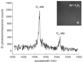
1520 1525 1530 1535 1540 1545 1550 wavelength (nm) 0 200 400 600 800 1000 1200 1400 Er photoluminescence (count) C2 site C3i site Si Er3+:Y 2O3
FIG. 4: Photoluminescence of Er3+in an epitaxial Y2O3film
grown on silicon using molecular beam epitaxy. Two optical transitions confirm the correct crystal symmetry site occu-pancies. The inset shows a transmission electron microscope image of the Y2O3 lattice on silicon.
wafers,5D
0 level lifetimes reached 0.8 ms, close to bulk
values. The 7F
0 →5D0 inhomogeneous linewidth was
about 200 GHz, a factor of 2 larger than expected from studies on transparent ceramics [96]. This could be due to stress in the film induced by differences in thermal expansion coefficients between silicon and Y2O3, which
would also explain the shift of the line with the annealing temperature. It may also stem from the presence of de-fects at grain boundaries since grain size in such polycrys-talline thin films is of the order of 30 nm. Ultra-thin films, which are of interest for dopant localization and hybrid devices [54], have also been investigated [102]. In films as thin as 7 nm, Er3+ luminescence at 1.5 µm showed
decay times of about 1.5 ms, a long value for Er3+
nano-materials, although still shorter than the 7.7 ms of bulk Er3+:Y
2O3. Further studies on coherent properties are
needed to assert the potential of these systems for quan-tum technologies, which may require specific setups such as waveguides to deal with film/substrate geometries and the low number of active ions in very thin layers [103]. The simple chemical composition and stable cubic phase of Y2O3 makes it possible to grow wafer-scale, epitaxial
thin films. Indeed, single crystal, epitaxial Y2O3 have
been synthesized using molecular beam epitaxy (MBE) on silicon wafers for high-k dielectric gate in MOSFET [104, 105]. Recently, this process has been improved to achieve exceptional qualities of Y2O3 films doped with
Er3+ [106]. Controls of doping concentrations in the
range of 1 to 100 parts per millions can be achieved. The thickness of the film up to 1.5 µm is also controllable with a precision down to a monolayer of atoms. The growth occurs via a two-dimensional layer-by-layer growth mode, resulting in smooth, uniform films, which offers several
distinct advantages: first, the epitaxial film has signif-icantly less optical loss and suggests better coherence for dopants; second, it allows atomic precision place-ment of rare-earth dopants via delta doping; third, the wafer-size film allows scalable top-down device pattern-ing uspattern-ing standard lithography and etchpattern-ing techniques. The photoluminescence of Er3+ was measured, which
clearly showed two distinct transitions corresponding to two crystal symmetry sites: C2 site at 1532 nm and C3i at 1542 nm. The wavelengths of the peaks agree with that in bulk Er3+:Y
2O3 [107], confirming the correct Y
site occupancies. Optical lifetimes and ground-state elec-tron paramagnetic resonance were measured [106]. The photoluminescence decay gives a T1of 8.7 ms for C2 site,
in excellent agreement with bulk Er3+:Y2O3
measure-ment [107]. Optical and spin coherence are next experi-ments to fully characterize this epitaxial film material.
Hybrid rare-earth materials
Other hybrid architectures have been considered, based on thin films or nanoparticles. A first example is the electrical control of coupling between rare-earth ions and a graphene layer [54]. Depending on the Fermi level in graphene, rare-earth can decay through photon emis-sion, non-radiatively by creation of electron-hole pairs in the graphene layer or by excitation of graphene plasmons. This process however is only efficient at distances below 10 nm and is therefore maximized for very thin rare-earth doped films. This effect was observed in a Er3+:Y
2O3
thin film of about 60 nm thickness obtained by the metal organic decomposition method on a Si substrate [108]. A graphene layer was placed on top of the film and covered by a transparent solid polymer electrolyte to allow tun-ing of graphene Fermi level by a gate voltage. Compartun-ing Er3+ emission below or outside the graphene sheet as a function of the voltage applied to the device, it was pos-sible to identify a regime of low emission in which Er3+ is quenched by the graphene, a stronger emission when electron hole pair creation becomes reduced and finally a low emission again when Er3+ is able to excite plasmon
in the graphene layer [54]. This demonstrates a unique capability of electrically controlling the local density of optical states of an emitter. The on-demand coupling of emitters with plasmons opens promising possibilities for quantum optoelectronics, which could take advantage of the coherence properties of rare-earth transitions. This will require large couplings that could be obtained with thinner films, provided that rare-earth properties can be preserved (see above, [102]).
A second example is the incorporation of rare-earth ions in diamond, one of the major material for quantum technologies. Such a system could combine the excellent properties of diamond such as high purity and crystalline quality with the narrow lines of rare-earth ions.
More-over, diamond can host a variety of defects with strong emissions and/or carrying spins with long coherence life-times that could also interact with rare-earths in hybrid quantum systems. Incorporating rare-earth ions, which have a large ionic radius, into the diamond lattice is how-ever difficult. One approach is to chemically self-assemble rare-earth complexes on bulk or nano-diamonds before growing a new diamond layer by CVD [109, 110]. An-other one consist in implanting rare-earth into bulk or nano diamond [111, 112]. Rare-earth ions luminescence has been observed with these different methods, with long lifetimes in the case of Eu3+ ions [109]. The lack of
well resolved crystal field structure in the spectra how-ever prevents a detailed analysis of the rare-earth local environment and comparison with simulations [109–111], which could unambiguously confirm their incorporation into diamond, still under debate [110]. High-resolution or coherent spectroscopy has not yet been reported on these systems.
OUTLOOK
Future advances in rare-earth nanophotonics hinges on breakthroughs in material synthesis, control and en-gineering. A set of material properties forms the key metrics for guiding this material development and op-timization. For nanocrystals, the particle size should be small enough for precise localization of the emitter with respective to the optical field it couples to, while large enough to suppress unwanted decoherence due to proximity to particle surfaces. For thin films, well con-trolled thickness and surface roughness are important for high quality photonic devices. The dopant spectro-scopic properties, including narrow optical and spin in-homogeneous linewidths, optical lifetimes, in-homogeneous linewidth, long spin T1 and T2, will continue to be the
qualifying parameters that drive the growth optimization process. Some of these parameters are less restrictive than others for specific applications. For instance, for single ion devices, inhomogeneous broadening is of sec-ondary concern as long as individual ion exhibits long-lived coherence.
One decisively enabling capabilities for rare-earth nanophotonics is the deterministic control of doping con-centration and placement in host matrices. The former is notoriously difficult in bulk, yttrium-based doped crys-tals, because the background doping of all sorts of rare-earth elements is at ∼ppm level in the raw yttrium ma-terial. This limitation might be overcome with less com-mon growth techniques such as floating zone growth or molecular beam epitaxy in which elements of rare-earths and yttrium can be better separated by their disparate vapor pressures or other physical properties. In terms of dopant placement, ALD and MBE offers powerful delta-doping options to precisely control the distance of dopant
to material interfaces, and in principle could result in a mono layer thickness of the doped material. The mas-tery of 2D film growth technique will further spur new ways to control dopant placement in 3D, for instance, by combining delta-doping with aperture-masked doping at prescribed locations on the substrate. With nanocrystals containing one or a few rare-earth ions, its placement can be controlled by functionalizing the substrate surface and chemically docking the nanocrystal to the desired loca-tion.
Once the above metrics and capabilities are realized, they open up powerful tools to nanoscopically control and tailor interactions of rare-earth ions with other quan-tum degrees of freedoms. With regard to nanophoton-ics, such controls will enable unprecedented enhancement of light-matter interaction at single rare-earth ion level, and potentially unlock new coupling modalities such as rare-earth-phonon, rare-earth-electric field interactions at varying length and energy scales. Together, these new rare-earth materials and accompanying processing tech-niques present an exciting prospect of engineering highly coherent quantum systems with on demand functionality and performance.
We would like to acknowledge D. Serrano and A. Tal-laire for their comments on the manuscript. This project has received funding from the National Science Founda-tion EAGER award No 1843044, European Union’s Hori-zon 2020 research and innovation programme under grant agreement No 712721 (NanOQTech).
[1] R. M. Macfarlane, “High-resolution laser spectroscopy of rare-earth doped insulators: a personal perspective,” Journal of Luminescence, vol. 100, no. 1, pp. 1 – 20, 2002.
[2] P. Goldner, A. Ferrier, and O. Guillot-No¨el, “Rare Earth-Doped Crystals for Quantum Information Pro-cessing ,” in Handbook on the Physics and Chemistry of Rare Earths (J.-C. G. B¨unzli and V. K. Pecharsky, eds.), pp. 1–78, Amsterdam: Elsevier, 2015.
[3] C. Thiel, T. Bttger, and R. Cone, “Rare-earth-doped materials for applications in quantum information stor-age and signal processing,” Journal of Luminescence, vol. 131, no. 3, pp. 353 – 361, 2011. Selected papers from DPC’10.
[4] Y. Sun, C. W. Thiel, R. Cone, R. Equall, and R. Hutch-eson, “Recent progress in developing new rare earth ma-terials for hole burning and coherent transient applica-tions,” Journal of Luminescence, vol. 98, no. 1, pp. 281 – 287, 2002. Proceedings of the Seventh International Meeting on Hole Burning, Single Molecules and Related Spectroscopies: Science and Applications.
[5] N. Kunkel and P. Goldner, “Recent Advances in Rare Earth Doped Inorganic Crystalline Materials for Quan-tum Information Processing,” Z. anorg. allg. Chem., vol. 644, pp. 66–76, Feb. 2018.
[6] M. Zhong, M. P. Hedges, R. L. Ahlefeldt, J. G.
Bartholomew, S. E. Beavan, S. M. Wittig, J. J. Longdell, and M. J. Sellars, “Optically addressable nu-clear spins in a solid with a six-hour coherence time,” Nature, vol. 517, pp. 177 EP –, 01 2015.
[7] M. Ranˇci´c, M. P. Hedges, R. L. Ahlefeldt, and M. J. Sellars, “Coherence time of over a second in a telecom-compatible quantum memory storage material,” Nature Physics, vol. 14, pp. 50 EP –, 09 2017.
[8] I. Usmani, M. Afzelius, H. de Riedmatten, and N. Gisin, “Mapping multiple photonic qubits into and out of one solid-state atomic ensemble,” Nature Commun, vol. 1, p. 12, 2010.
[9] N. Sinclair, E. Saglamyurek, H. Mallahzadeh, J. A. Slater, M. George, R. Ricken, M. P. Hedges, D. Oblak, C. Simon, W. Sohler, and W. Tittel, “Spectral multi-plexing for scalable quantum photonics using an atomic frequency comb quantum memory and feed-forward control,” Phys. Rev. Lett., vol. 113, p. 053603, Jul 2014. [10] W. Tittel, M. Afzelius, T. Chaneli´ere, R. Cone, S. Kr´oll, S. Moiseev, and M. Sellars, “Photon-echo quantum memory in solid state systems,” Laser & Photonics Re-views, vol. 4, no. 2, pp. 244–267, 2010.
[11] A. I. Lvovsky, B. C. Sanders, and W. Tittel, “Optical quantum memory,” Nature Photonics, vol. 3, pp. 706– 714, 12 2009.
[12] J. J. Longdell, E. Fraval, M. J. Sellars, and N. B. Man-son, “Stopped light with storage times greater than one second using electromagnetically induced transparency in a solid,” Phys. Rev. Lett, vol. 95, p. 063601, 2005. [13] G. Heinze, C. Hubrich, and T. Halfmann, “Stopped light
and image storage by electromagnetically induced trans-parency up to the regime of one minute,” Phys. Rev. Lett, vol. 111, p. 033601, 2013.
[14] C. Clausen, I. Usmani, F. Bussi`eres, N. Sangouard, M. Afzelius, H. de Riedmatten, and N. Gisin, “Quantum storage of photonic entanglement in a crystal,” Nature, vol. 469, pp. 508–511, 2011.
[15] F. Bussi`eres, C. Clausen, A. Tiranov, B. Korzh, V. B. Verma, S. W. Nam, F. Marsili, A. Ferrier, P. Goldner, H. Herrmann, C. Silberhorn, W. Sohler, M. Afzelius, and N. Gisin, “Quantum teleportation from a telecom-wavelength photon to a solid-state quantum memory,” Nature Photon., vol. 8, pp. 775–778, 2014.
[16] E. Saglamyurek, N. Sinclair, J. Jin, J. A. Slater, D. Oblak, F. Bussi`eres, M. George, R. Ricken, W. Sohler, and W. Tittel, “Broadband waveguide quan-tum memory for entangled photons,” Nature, vol. 469, pp. 512–515, 01 2011.
[17] H. de Riedmatten, M. Afzelius, M. U. Staudt, C. Simon, and N. Gisin, “A solid-state light–matter interface at the single-photon level,” Nature, vol. 456, pp. 773 EP –, 12 2008.
[18] Z.-Q. Zhou, W.-B. Lin, M. Yang, C.-F. Li, and G.-C. Guo, “Realization of reliable solid-state quantum mem-ory for photonic polarization qubit,” Phys. Rev. Lett, vol. 180, p. 190505, 2012.
[19] T. Zhong, J. M. Kindem, J. G. Bartholomew, J. Rochman, I. Craiciu, V. Verma, S. W. Nam, F. Marsili, M. D. Shaw, A. D. Beyer, and A. Faraon, “Nanophotonic rare-earth quantum memory with opti-cally controlled retrieval,” Science, vol. 357, pp. 1392– 1395, 2016.
[20] P. Jobez, C. Laplane, N. Timoney, N. Gisin, A. Ferrier, P. Goldner, and M. Afzelius, “Coherent Spin Control
at the Quantum Level in an Ensemble-Based Optical Memory,” Phys. Rev. Lett., vol. 114, p. 230502, June 2015.
[21] J. J. Longdell and M. J. Sellars, “Demonstration of con-ditional quantum phase shift between ions in a solid,” Phys. Rev. A, vol. 69, p. 032307, 2004.
[22] M. P. Hedges, J. J. Longdell, Y. Li, and M. J. Sellars, “Efficient quantum memory for light,” Nature, vol. 465, pp. 1052–1056, 2010.
[23] M. Afzelius, I. Usmani, A. Amari, B. Lauritzen, A. Walther, C. Simon, N. Sangouard, J. c. v. Min´aˇr, H. de Riedmatten, N. Gisin, and S. Kr¨oll, “Demonstra-tion of atomic frequency comb memory for light with spin-wave storage,” Phys. Rev. Lett., vol. 104, p. 040503, 2010.
[24] M. Sabooni, Q. Li, S. Kr¨oll, and L. Rippe, “Efficient quantum memory using a weakly absorbing sample,” Phys. Rev. Lett, vol. 110, p. 133604, 2013.
[25] N. Maring, P. Farrera, K. Kutluer, M. Mazzera, G. Heinze, and H. de Riedmatten, “Photonic quantum state transfer between a cold atomic gas and a crystal,” Nature, vol. 551, no. 7681, pp. 485–488, 2017.
[26] G. Wolfowicz, H. Maier-Flaig, R. Marino, A. Ferrier, H. Vezin, J. J. L. Morton, and P. Goldner, “Coherent storage of microwave excitations in rare earth nuclear spins,” Phys. Rev. Lett., vol. 114, p. 170503, 2015. [27] C. O. Brien, N. Lauk, S. Blum, G. Morigi, and M.
Fleis-chhauer, “Interfacing superconducting qubits and tele-com photons via a rare-earth-doped crystal,” Phys. Rev. Lett, vol. 113, p. 063603, 2014.
[28] L. A. Williamson, C. Y.-H., and J. J. Longdell, “Magneto-optic modulator with unit quantum effi-ciency,” Phys. Rev. Lett, vol. 113, p. 203601, 2014. [29] S. Probst, H. Rotzinger, S. W¨unsch, P. Jung,
M. Jerger, M. Siegel, A. V. Ustinov, and P. A. Bu-shev, “Anisotropic rare-earth spin ensemble strongly coupled to a superconducting resonator,” Phys. Rev. Lett, vol. 110, p. 157001, 2013.
[30] G. Dold, C. W. Zollitsch, J. O’Sullivan, S. Welinski, A. Ferrier, P. Goldner, S. de Graaf, T. Lindstr¨om, and J. J. Morton, “High-cooperativity coupling of a rare-earth spin ensemble to a superconducting resonator us-ing yttrium orthosilicate as a substrate,” Phys. Rev. Ap-plied, vol. 11, p. 054082, 2019.
[31] X. Fernandez-Gonzalvo, Y.-H. Chen, C. Yin, S. Rogge, and J. J. Longdell, “Coherent frequency up-conversion of microwaves to the optical telecommunications band in an er:yso crystal,” Phys. Rev. A, vol. 6, p. 062313, 2015.
[32] X. Fernandez-Gonzalvo, Y.-H. Chen, C. Yin, S. Rogge, and J. J. Longdell, “Cavity enhanced raman heterodyne spectroscopy in er:yso for microwave to optical signal conversion,” arXiv: 1712.07735, 2017.
[33] J. M. Kindem, J. G. Bartholomew, P. J. T. Wood-burn, T. Zhong, I. Craiciu, R. L. Cone, C. W. Thiel, and A. Faraon, “Characterization of171Yb3+: yvo4 for
photonic quantum technologies,” Phys. Rev. B, vol. 98, p. 024404, Jul 2018.
[34] C. O. Brien, T. Zhong, A. Faraon, and C. Simon, “Non-destructive photon detection using a single rare-earth ion coupled to a photonic cavity,” Phys. Rev. A, vol. 94, p. 043807, 2016.
[35] R. Kolesov and et al., “Optical detection of a single rare-earth ion in a crystal,” Nat. Commun., vol. 3, p. 1029,
2012.
[36] T. Utikal, E. Eichhammer, L. Petersen, A. Renn, S. G¨otzinger, and V. Sandoghdar, “Spectroscopic de-tection and state preparation of a single praseodymium ion in a crystal,” Nat. Commun., vol. 5, p. 3627, 2014. [37] I. Nakamura, T. Yoshihiro, H. Inagawa, S. Fujiyoshi,
and M. Matsushita, “Spectroscopy of single pr3+ion in laf3 crystal at 1.5 k,” Sci. Rep, vol. 4, p. 7364, 2014.
[38] R. Kolesov, K. Xia, R. Reuter, M. Jamali, R. St¨ohr, T. Inal, P. Siyushev, and J. Wrachtrup, “Mapping spin coherence of a single rare-earth ion in a crystal onto a single photon polarization state,” Phys. Rev. Lett., vol. 111, p. 120502, 2013.
[39] P. Siyushev, K. Xia, R. Reuter, M. Jamali, N. Zhao, N. Yang, C. Duan, N. Kukharchyk, A. D. Wieck, R. Kolesov, and J. Wrachtrup, “Coherent properties of single rare-earth spin qubits.,” Nat. Commun., vol. 5, p. 3895, 2014.
[40] K. Xia, R. Kolesov, Y. Wang, P. Siyushev, R. Reuter, T. Kornher, N. Kukharchyk, A. D. Wieck, B. Villa, S. Yang, and J. Wrachtrup, “All-optical preparation of coherent dark states of a single rare earth ion spin in a crystal,” Phys. Rev. Lett., vol. 115, p. 93602, 2015. [41] T. Zhong, J. M. Kindem, J. G. Bartholomew,
J. Rochman, I. Craiciu, V. Verma, S. W. Nam, F. Mar-sili, M. D. Shaw, A. D. Beyer, and A. Faraon, “Optically addressing single rare-earth ions in a nanophotonic cav-ity,” Phys. Rev. Lett., vol. 121, p. 183603, 2018. [42] C. Yin, M. Rancic, G. G. de Boo, N. Stavrias, J. C.
McCallum, M. J. Sellars, and S. Rogge, “Optical ad-dressing of an individual erbium ion in silicon,” Nature, vol. 497, pp. 91–95, 2013.
[43] A. Dibos, M. Raha, C. Phenicie, and J. Thompson, “Atomic source of single photons in the telecom band,” Phys. Rev. Lett, vol. 120, p. 243601, 2018.
[44] N. Sinclair, D. Oblak, C. W. Thiel, R. L. Cone, and W. Tittel, “Properties of a rare-earth-ion-doped waveg-uide at sub-kelvin temperatures for quantum signal pro-cessing,” Phys. Rev. Lett, vol. 118, p. 100, 2017. [45] M. F. Askarani, M. G. Puigibert, T. Lutz, V. B.
Verma, M. D. Shaw, S. W. Nam, N. Sinclair, D. Oblak, and W. Tittel, “Storage and reemission of heralded telecommunication-wavelength photons using a crystal waveguide,” Phys. Rev. Applied, vol. 11, p. 054056, 2019.
[46] G. Corrielli, A. Seri, M. Mazzera, R. Osellame, and H. de Riedmatten, “Integrated optical memory based on laser-written waveguides,” Phys. Rev. Applied, vol. 5, p. 054013, May 2016.
[47] S. Marzban, J. G. Bartholomew, S. Madden, K. Vu, and M. J. Sellars, “Observation of photon echoes from evanescently coupled rare-earth ions in a planar waveg-uide,” Phys. Rev. Lett., vol. 115, p. 013601, Jul 2015. [48] E. Miyazono, I. Craiciu, A. Arbabi, T. Zhong, and
A. Faraon, “Coupling erbium dopants in yttrium or-thosilicate to silicon photonic resonators and waveg-uides,” Opt. Express, vol. 25, pp. 2863–2871, 2017. [49] D. Ding, L. M. C. Pereira, J. F. Bauters, M. J. R.
Heck, G. Welker, A. Vantomme, J. E. Bowers, M. J. A. de Dood, and D. Bouwmeester, “Multidimensional pur-cell effect in an ytterbium-doped ring resonator,” Nat. Photonics, vol. 10, pp. 385–388, 2016.
[50] D. L. McAuslan and J. J. Longdell, “Strong-coupling cavity qed using rare-earth-metal-ion dopants in
mono-lithic resonators: What you can do with a weak oscilla-tor,” Phys. Rev. A, vol. 80, p. 062307, 2009.
[51] T. Zhong, J. M. Kindem, E. Miyazono, and A. Faraon, “Nanophotonic coherent light-matter interfaces based on rare-earth doped crystals,” Nat. Commun, vol. 6, p. 8206, 2015.
[52] T. Zhong, J. Rochman, J. M. Kindem, E. Miyazono, and A. Faraon, “High quality factor nanophotonic res-onators in bulk rare-earth doped crystals,” Opt. Ex-press, vol. 24, pp. 536–544, 2016.
[53] T. Zhong, J. M. Kindem, J. Rochman, and A. Faraon, “Interfacing broadband photonic qubits to a cavity-protected rare-earth ensemble,” Nat. Commun, vol. 8, p. 14107, 2017.
[54] K. J. Tielrooij, L. Orona, A. Ferrier, M. Badioli, G. Nav-ickaite, S. Coop, S. Nanot, B. Kalinic, T. Cesca, L. Gau-dreau, Q. Ma, A. Centeno, A. Pesquera, A. Zurutuza, H. de Riedmatten, P. Goldner, F. J. G. de Abajo, P. Jarillo-Herrero, and F. H. L. Koppens, “Electrical control of optical emitter relaxation pathways enabled by graphene,” Nat. Phys., vol. 11, pp. 281–287, Mar. 2015.
[55] H. Zhang, J. Yang, S. Gray, J. A. Brown, T. D. Ketcham, D. E. Baker, A. Carapella, R. W. Davis, J. G. Arroyo, and D. A. Nolan, “Transparent Er3+-Doped Y2O3 Ceramics with Long Optical Coherence Lifetime,” ACS Omega, vol. 2, pp. 3739–3744, July 2017.
[56] A. Perrot, P. Goldner, D. Giaume, M. Lovri´c, C. Andri-amiadamanana, R. R. Gon¸calves, and A. Ferrier, “Nar-row Optical Homogeneous Linewidths in Rare Earth Doped Nanocrystals,” Phys. Rev. Lett., vol. 111, no. 20, p. 203601, 2013.
[57] R. Kolesov, K. Xia, R. Reuter, R. St¨ohr, A. Zappe, J. Meijer, P. R. Hemmer, and J. Wrachtrup, “Optical detection of a single rare-earth ion in a crystal,” Nat. Commun., vol. 3, p. 1029, 2012.
[58] B. Casabone, J. Benedikter, T. H¨ummer, F. Oehl, K. de Oliveira Lima, T. W. H¨ansch, A. Ferrier, P. Goldner, H. de Riedmatten, and D. Hunger, “Cavity-enhanced spectroscopy of a few-ion ensemble in Eu3+:Y2O3,” New J. Phys., vol. 20, pp. 095006–9, Sept. 2018.
[59] J. Yang, Z. Quan, D. Kong, X. Liu, and J. Lin, “Y2O3: Eu3+Microspheres: Solvothermal Synthesis and Luminescence Properties,” Cryst. Growth Des., vol. 7, pp. 730–735, Apr. 2007.
[60] I. D. Abella, N. A. Kurnit, and S. R. Hartmann, “Pho-ton echoes,” Phys. Rev., vol. 141, no. 1, p. 391, 1966. [61] R. S. Meltzer, “Line Broadening Mechanisms and Their
Measurement,” in Spectroscopic properties of rare earths in optical materials (B. Jacquier and G. Liu, eds.), pp. 191–265, Springer, 2005.
[62] F. Beaudoux, A. Ferrier, O. Guillot-No¨el, T. Chaneli`ere, J.-L. Le Gou¨et, and P. Goldner, “Emission of photon echoes in a strongly scattering medium,” Opt. Express, vol. 19, no. 16, pp. 15236–15243, 2011.
[63] R. Pierrat, R. Carminati, and J.-L. Le Gou¨et, “Photon echoes in strongly scattering media: A diagrammatic approach,” Phys. Rev. A, vol. 97, pp. 645–12, June 2018. [64] R. S. Meltzer and K. Hong, “Electron-phonon interac-tions in insulating nanoparticles: Eu2O3,” Phys. Rev. B, vol. 61, pp. 3396–3403, Feb. 2000.
[65] C. W. Thiel, R. M. Macfarlane, Y. Sun, T. B¨ottger, N. Sinclair, W. Tittel, and R. L. Cone in Quantum Light
Matter Interaction in Solid State Systems, (Barcelona), 2015.
[66] N. Kunkel, J. Bartholomew, S. Welinski, A. Ferrier, A. Ikesue, and P. Goldner, “Dephasing mechanisms of optical transitions in rare-earth-doped transparent ce-ramics,” Phys. Rev. B, vol. 94, p. 184301, Nov. 2016. [67] G. P. Flinn, K. W. Jang, J. Ganem, M. L. Jones,
R. S. Meltzer, and R. M. Macfarlane, “Sample-dependent optical dephasing in bulk crystalline samples of Y2O3:Eu3+,” Phys. Rev. B, vol. 49, no. 9, p. 5821,
1994.
[68] S. Sohn, Y. Kwon, Y. Kim, and D. Kim, “Synthesis and characterization of near-monodisperse yttria par-ticles by homogeneous precipitation method,” Powder Technol., vol. 142, pp. 136–153, Apr. 2004.
[69] K. de Oliveira Lima, R. Rocha Gon¸calves, D. Giaume, A. Ferrier, and P. Goldner, “Influence of defects on sub-˚
A optical linewidths in Eu3+:Y2O3 particles,” J. Lu-min., vol. 168, pp. 276–282, Dec. 2015.
[70] J. G. Bartholomew, K. de Oliveira Lima, A. Ferrier, and P. Goldner, “Optical Line Width Broadening Mecha-nisms at the 10 kHz Level in Eu3+:Y2O3 Nanoparti-cles,” Nano. Lett., vol. 17, pp. 778–787, Jan. 2017. [71] M. Kim, H. J. Mamin, M. H. Sherwood, K. Ohno,
D. D. Awschalom, and D. Rugar, “Decoherence of Near-Surface Nitrogen-Vacancy Centers Due to Electric Field Noise,” Phys. Rev. Lett., vol. 115, p. 087602, Aug. 2015. [72] S. Liu, D. Serrano, A. Fossati, A. Tallaire, A. Ferrier, and P. Goldner, “Controlled size reduction of rare earth doped nanoparticles for optical quantum technologies,” RSC Adv., vol. 8, pp. 37098–37104, Nov. 2018.
[73] A. Walther, L. Rippe, Y. Yan, J. Karlsson, D. Serrano, A. N. Nilsson, S. Bengtsson, and S. Kr¨oll, “High-fidelity readout scheme for rare-earth solid-state quantum com-puting,” Phys. Rev. A, vol. 92, p. 022319, Aug. 2015. [74] S. Hartmann, “Photon, spin, and Raman echoes,” IEEE
J. Quantum Electron., vol. 4, pp. 802–807, Nov. 1968. [75] B. S. Ham, M. S. Shahriar, M. K. Kim, and P. R.
Hem-mer, “Spin coherence excitation and rephasing with op-tically shelved atoms,” Phys. Rev. B, vol. 58, no. 18, pp. 11825–11828, 1998.
[76] O. Guillot-No¨el, P. Goldner, F. Beaudoux, Y. Le Du, J. Lejay, A. Amari, A. Walther, L. Rippe, and S. Kr¨oll, “Hyperfine structure and hyperfine coherent properties of praseodymium in single-crystalline La2(WO4)3 by
hole-burning and photon-echo techniques,” Phys. Rev. B, vol. 79, no. 15, p. 155119, 2009.
[77] D. Serrano, J. Karlsson, A. Fossati, A. Ferrier, and P. Goldner, “All-optical control of long-lived nuclear spins in rare-earth doped nanoparticles,” Nat. Com-mun., vol. 9, p. 2127, May 2018.
[78] J. Karlsson, N. Kunkel, A. Ikesue, A. Ferrier, and P. Goldner, “Nuclear spin coherence properties of 151Eu3+ and 153Eu3+ in a Y2O3 transparent ce-ramic,” J. Phys.: Condens. Matter, vol. 29, p. 125501, Mar. 2017.
[79] J. J. Longdell, A. Alexander, and M. J. Sellars, “Char-acterization of the hyperfine interaction in europium-doped yttrium orthosilicate and europium chloride hex-ahydrate,” Phys. Rev. B, vol. 74, p. 195101, Nov. 2006. [80] R. L. Ahlefeldt, M. Zhong, J. G. Bartholomew, and M. J. Sellars, “Minimizing Zeeman sensitivity on optical and hyperfine transitions in EuCl3 6H2O to extend
[81] E. Z. Cruzeiro, J. Etesse, A. Tiranov, P.-A. Bourdel, F. Fr¨owis, P. Goldner, N. Gisin, and M. Afzelius, “Char-acterization of the hyperfine interaction of the excited
5
D0 state of Eu3+:Y2SiO5,” Phys. Rev. B, vol. 97,
p. 094416, Mar. 2018.
[82] R. M. Macfarlane, “Optical Stark spectroscopy of solids,” J. Lumin., vol. 125, no. 1-2, pp. 156–174, 2007. [83] R. M. Macfarlane, A. Arcangeli, A. Ferrier, and P. Gold-ner, “Optical Measurement of the Effect of Electric Fields on the Nuclear Spin Coherence of Rare-Earth Ions in Solids,” Phys. Rev. Lett., vol. 113, no. 15, p. 157603, 2014.
[84] E. Fraval, M. J. Sellars, and J. J. Longdell, “Method of Extending Hyperfine Coherence Times in Pr3+:Y2SiO5,” Phys. Rev. Lett., vol. 92, no. 7, p. 077601, 2004.
[85] P. Goldner, O. Guillot-No¨el, F. Beaudoux, Y. Le Du, J. Lejay, T. Chaneli`ere, L. Rippe, A. Amari, A. Walther, and S. Kr¨oll, “Long coherence lifetime and electro-magnetically induced transparency in a highly-spin-concentrated solid,” Phys. Rev. A, vol. 79, no. 3, p. 033809, 2009.
[86] O. Guillot-No¨el, Y. Le Du, F. Beaudoux, E. Antic-Fidancev, M. F. Reid, R. A. Marino, J. Lejay, and P. Goldner, “Calculation and analysis of hyperfine and quadrupole interactions in praseodymium-doped La2(WO4)3,” J. Lumin., vol. 130, no. 9, pp. 1557–1565,
2010.
[87] M. Lovri´c, P. Glasenapp, D. Suter, B. Tumino, A. Fer-rier, P. Goldner, M. Sabooni, L. Rippe, and S. Kr¨oll, “Hyperfine characterization and spin coherence lifetime extension in Pr3+:La
2(WO4)3,” Phys. Rev. B, vol. 84,
no. 10, p. 104417, 2011.
[88] R. S. Meltzer, W. Yen, H. Zheng, S. Feofilov, M. De-jneka, B. Tissue, and H. Yuan, “Evidence for long-range interactions between rare-earth impurity ions in nanocrystals embedded in amorphous matrices with the two-level systems of the matrix,” Phys. Rev. B, vol. 64, p. 100201, Aug. 2001.
[89] E. Eichhammer, T. Utikal, S. G¨otzinger, and V. San-doghdar, “Spectroscopic detection of single Pr3+ ions on the 3H4 1D2 transition,” New J. Phys., vol. 17, pp. 1–7, Aug. 2015.
[90] T. Lutz, L. Veissier, C. W. Thiel, P. J. T. Woodburn, R. L. Cone, P. E. Barclay, and W. Tittel, “Effects of fab-rication methods on spin relaxation and crystallite qual-ity in Tm-doped powders studied using spectral hole burning,” Sci. Technol. Adv. Mater., vol. 17, pp. 63–70, July 2016.
[91] T. Lutz, L. Veissier, C. W. Thiel, P. J. T. Woodburn, R. L. Cone, P. E. Barclay, and W. Tittel, “Effects of mechanical processing and annealing on optical coher-ence properties of Er3+:LiNbO3 powders,” J. Lumin., vol. 191, pp. 2–12, 2017.
[92] A. Ikesue and Y. L. Aung, “Synthesis and Performance of Advanced Ceramic Lasers,” J. Am. Ceram. Soc., vol. 89, pp. 1936–1944, June 2006.
[93] A. Ikesue and Y. L. Aung, “Ceramic laser materials,” Nat. Photonics, vol. 2, pp. 721–727, 2008.
[94] S. Liu, J. A. Mares, X. Feng, A. Vedda, M. Fasoli, Y. Shi, H. Kou, A. Beitlerova, L. Wu, C. D’Ambrosio, Y. Pan, and M. Nikl, “Towards Bright and Fast Lu3Al5O12:Ce,Mg Optical Ceramics Scintillators,” Ad-vanced Optical Materials, vol. 4, pp. 731–739, May 2016.
[95] A. Ferrier, C. W. Thiel, B. Tumino, M. O. Ram´ırez, L. E. Baus´a, R. L. Cone, A. Ikesue, and P. Gold-ner, “Narrow inhomogeneous and homogeneous optical linewidths in a rare earth doped transparent ceramic,” Phys. Rev. B, vol. 87, no. 4, p. 041102, 2013.
[96] N. Kunkel, A. Ferrier, C. W. Thiel, M. O. Ram´ırez, L. E. Baus´a, R. L. Cone, A. Ikesue, and P. Goldner, “Rare-earth doped transparent ceramics for spectral filter-ing and quantum information processfilter-ing,” APL Mater., vol. 3, pp. 096103–7, Sept. 2015.
[97] N. Kunkel, J. Bartholomew, L. Binet, A. Ikesue, and P. Goldner, “High-Resolution Optical Line Width Mea-surements as a Material Characterization Tool,” J. Phys. Chem. C, vol. 120, pp. 13725–13731, June 2016. [98] A. L. Alexander, J. J. Longdell, and M. J. Sellars,
“Mea-surement of the ground-state hyperfine coherence time of151Eu3+:Y2SiO5,” J. Opt. Soc. Am. B, vol. 24, no. 9,
pp. 2479–2482, 2007.
[99] A. Arcangeli, M. Lovri´c, B. Tumino, A. Ferrier, and P. Goldner, “Spectroscopy and coherence lifetime exten-sion of hyperfine transitions in151Eu3+:Y2SiO5,” Phys.
Rev. B, vol. 89, no. 18, p. 184305, 2014.
[100] T. B¨ottger, C. W. Thiel, Y. Sun, and R. L. Cone, “Op-tical decoherence and spectral diffusion at 1.5µm in Er3+:Y
2SiO5 versus magnetic field, temperature, and
Er3+ concentration,” Phys. Rev. B, vol. 73, no. 7, p. 075101, 2006.
[101] V. Miikkulainen, M. Leskel¨a, M. Ritala, and R. L. Puu-runen, “Crystallinity of inorganic films grown by atomic layer deposition: Overview and general trends,” J. Appl. Phys., vol. 113, pp. 021301–102, Jan. 2013.
[102] M. Scarafagio, A. Tallaire, K.-J. Tielrooij, D. Cano, A. Grishin, M.-H. Chavanne, F. H. L. Koppens, A. Ringued´e, M. Cassir, D. Serrano, P. Goldner, and A. Ferrier, “Ultrathin Eu- and Er-Doped Y2O3 Films with Optimized Optical Properties for Quantum Tech-nologies,” J. Phys. Chem. C, vol. 123, pp. 13354–13364, May 2019.
[103] S. Marzban, J. G. Bartholomew, S. Madden, K. Vu, and M. J. Sellars, “Observation of Photon Echoes From Evanescently Coupled Rare-Earth Ions in a Planar Waveguide,” vol. 115, p. 013601, July 2015.
[104] S. Guha, E. Cartier, M. A. Gribelyuk, N. A. Bojar-czuk, and M. C. Copel, “Atomic beam deposition of lanthanum- and yttrium-based oxide thin films for gate dielectrics,” Appl. Phys. Lett, vol. 77, pp. 2710–2712, 2000.
[105] S. Guha, N. A. Bojarczuk, and V. Narayanan, “Lattice-matched, epitaxial, silicon-insulating lanthanum yt-trium oxide heterostructures,” Appl. Phys. Lett, vol. 80, pp. 766–768, 2002.
[106] K. A. M. Singh, T. Rajh, T. Zhong, and S. Guha, “Char-acterization of epitaxially grown erbium doped y2o3 for
quantum optics applications,” in Proceedings of APS March Meeting, (Boston MA, USA), P11.00008, 2019. [107] G. D. Reinemer, Optical characterization of perturned
sites in rare earth doped oxide crystals. PhD thesis, Montana State University, 2003.
[108] C. Andriamiadamanana, A. Ibanez, A. Ferrier, A.-L. Joudrier, L. Lombez, M. Liotaud, J.-F. Guillemoles, and F. Pell´e, “Erbium-doped yttria thin films prepared by metal organic decomposition for up-conversion,” Thin Solid Films, vol. 537, pp. 42–48, June 2013.
I. Aharonovich, “Synthesis of luminescent europium de-fectsin diamond,” Nat. Commun., vol. 5, pp. 1–6, Mar. 2014.
[110] D. E. P. Vanpoucke, S. S. Nicley, J. Raymakers, W. Maes, and K. Haenen, “Can europium atoms form luminescent centres in diamond A combined theoretical-experimental study,” Diam, Relat. Mat., vol. 94, pp. 233–241, Apr. 2019.
[111] J. Cajzl, P. Nekvindov´a, A. Mackov´a, P. Malinsk´y, D. Sedmidubsk´y, M. Huˇs´ak, Z. Remeˇs, M. Varga,
A. Kromka, R. B¨ottger, and J. Oswald, “Erbium ion im-plantation into diamond – measurement and modelling of the crystal structure,” Phys. Chem. Chem. Phys., vol. 19, pp. 6233–6245, Feb. 2017.
[112] J. Cajzl, B. Akhetova, P. Nekvindov´a, A. Mackov´a, P. Malinsk´y, J. Oswald, Z. Remeˇs, M. Varga, and A. Kromka, “Co-implantation of Er and Yb ions into single-crystalline and nano-crystalline diamond,” Surf Interface Anal, vol. 5, pp. 3523–6, Mar. 2018.
![FIG. 1: Evolving material platforms for rare-earth quantum devices from macroscopic bulk crystals (Reprinted from [10]) to low-dimensional materials including doped nanocrystals (Reprinted from [55]) and sub-micron thick films.](https://thumb-eu.123doks.com/thumbv2/123doknet/7771042.256900/4.918.101.429.514.678/evolving-platforms-macroscopic-reprinted-dimensional-materials-nanocrystals-reprinted.webp)