Any correspondence concerning this service should be sent to the repository administrator:
staff-oatao@inp-toulouse.fr
Identification number: DOI: 10.1016/j.jcrysgro.2014.09.032
Official URL:
http://dx.doi.org/10.1016/j.jcrysgro.2014.09.032
This is an author-deposited version published in:
http://oatao.univ-toulouse.fr/
Eprints ID: 13579
To cite this version:
Krisyuk, Vladislav V. and Shubin, Yuriy V. and Senocq, François and
Turgambaeva, Asiya E. and Duguet, Thomas and Igumenov, Igor K. and Vahlas,
Constantin
Chemical vapor deposition of Pd/Cu alloy films from a new single
source precursor
. (2015) Journal of Crystal Growth, vol. 414. pp. 130-134.
ISSN 0022-0248
O
pen
A
rchive
T
oulouse
A
rchive
O
uverte (
OATAO
)
OATAO is an open access repository that collects the work of Toulouse researchers and
makes it freely available over the web where possible.
Chemical vapor deposition of Pd/Cu alloy films from a new single
source precursor
Vladislav V. Krisyuk
a,n, Yuriy V. Shubin
a,c, François Senocq
b, Asiya E. Turgambaeva
a,
Thomas Duguet
b, Igor K. Igumenov
a, Constantin Vahlas
baNikolaev Institute of Inorganic Chemistry SB RAS, Pr. Acad. Lavrentiev 3, Novosibirsk 630090, Russia bCIRIMAT, ENSIACET, 4, allée Emile Monso, BP-44362, 31030 Toulouse Cedex 4, France
cNovosibirsk State University, 2, Pirogova Str., Novosibirsk 630090, Russia
Keywords:
A3. Metalorganic chemical vapor deposition A3. Polycrystalline deposition
B1. Metals
B3 Pd-alloy membranes
a b s t r a c t
Cu/Pd alloys were deposited onto Si(100) and SiO2(fused silica) substrates by MOCVD from PdL2CuL2, (L¼2-methoxy-2,6,6-trimethylheptane-3,5-dionate), a new single source bimetallic precursor. Deposi-tion was performed at 10 Torr in a temperature range between 200 1C and 350 1C and was assisted by vacuum ultraviolet (VUV) irradiation of the precursor vapor from an excimer Xe-lamp. It was shown that the elemental and phase composition of the films can be controlled by varying the deposition temperature and by stimulating by VUV the precursor decomposition. The bulk compositional properties of the obtained films confirmed the feasibility of proposed approach and precursor to prepare Pd alloy membrane materials by the CVD method.
1. Introduction
The increased demand for hydrogen in recent years has revived the interest in methods for separation and purification of hydrogen from gas mixtures in many sectors such as petroleum refining, petrochem-ical and semiconductor processing, as well as in new energy-related applications, especially in clean fuel for fuel cells and vehicles. Efficient hydrogen separation membrane alloys are characterized by high hydrogen permeability, low expansion when saturated with hydrogen, good corrosion resistance and high plasticity and strength during operation at temperatures in the range between 300 1C and 700 1C. The main concerns with membrane reliability are related to corrosion resistance and to structural modifications during operation resulting in change of hydrogen permeability. Pd alloy membranes with high selectivity for hydrogen and convenient thermal, chemical, and mec-hanical properties are widely used for this purpose [1]. Pd–Cu membranes are cost effective materials and have high resistance to sulfurous compounds in gas mixtures while maintaining a desirable set of properties[2–11]. It has been established that Pd47Cu53with B2
(bcc) structure shows higher permeability than Pd at 350oC; the
Pd–Cu B2 phase is not thermally stable and is subject to surface poisoning while fcc Pd–Cu alloys show some resistance to surface poisoning. Pd–Cu membranes exhibit better performance than Pd-sputtered membranes at high current densities in direct alcohol fuel
cells as a primary power source for stationary and portable devices
[12–15]. In a complementary perspective, electromigration resistant Pd/Cu alloy films have also been investigated in microelectronics as conductive or buffer layers in circuit design[16,17].
Up to now, many deposition techniques have been investigated to fabricate Pd–Cu composite films. However, to the best of the authors knowledge, there is actually no industrially implemented method of obtaining Pd membranes, each one having its problems yet unsolved. For example, wet deposition techniques like electro-less and electro deposition are electro-less suitable for the production of binary, ternary and multicomponent Pd-alloys due to difficulties in controlling the alloy composition and layer thickness on large areas. Processing of Pd–Cu and, more generally of intermetallic alloy coatings by metal organic chemical vapor deposition (MOCVD) is expected to extend their implementation in surface engineering. Especially, thanks to the possibility to operate in surface reaction controlled regime, MOCVD allows surface treatment of complex-in-shape items such as glass molds, turbine blades and vanes in aeronautic industries, or porous preforms whose internal surface may be functionalized for the preparation of supported catalysts. High growth rate, versatility, cost effectiveness, environmental compatibility, ease to scale up and the possibility to process films containing thermodynamically metastable phases, are additional advantages of MOCVD processes. Finally, the use of molecular precursors allows operating at low to moderate temperatures, thus extending the targeted applications spectrum so as to cover temperature-sensitive substrates.
http://dx.doi.org/10.1016/j.jcrysgro.2014.09.032
nCorresponding author.
The price to pay for this high potential is the need to tackle the challenges imposed by the complex gas phase and surface chemistries. In addition to mastering the deposition reaction, these challenges also concern the precursor design and delivery, in terms of non-toxicity, stability and volatility. The inherent difficulty for the establishment of a robust MOCVD process is further amplified in the case of coatings containing several elements and potentially intermetallic phases, mainly because of the limited width of their stability domains, the far-from-equilibrium initial state which can lead to unpredicted transitions and, last but not the least, of the requirement to use compatible precursors for the deposited elements[18]. Until now, this situa-tion resulted in limited investigasitua-tion of MOCVD for the co-deposisitua-tion of intermetallic alloy films. The above mentioned constraints can be partially circumvented if the preparation of the coating proceeds through the use of a single source precursor. In the case of Pd–Cu based membranes, it would be useful to dispose of a precursor providing deposition of the base Pd–Cu alloy when another compo-nent (e.g. Ag, Ru, V, Y, Zr, etc.) which is of minor content (several at%) can be codeposited from the separate compound.
In this perspective, the present contribution is focused on the investigation of PdL2CuL2, (L¼2-methoxy-2,6,6-trimethylhep-tane-3,5-dionate), an original single source, volatile precursor with a Pd/Cu ratio equal to one, for the CVD of Pd–Cu films. CVD of Pd–Cu films is performed under thermal activation. Moreover, vacuum ultraviolet activation of the input gas is combined with thermal activation with the aim to improve the film quality and/or to decrease the thermal budget of the process.
2. Experimental
Detailed information on the synthesis and the properties of [PdL2CuL2] will be published in the forthcoming paper. It is
recalled here that the compound can be sublimed in vacuum (130 1C, 10!2Torr) while preserving its composition and structure.
Pd–Cu films were deposited on Si(100) and fused silica 10 10 mm2substrates in a cold wall stainless steel CVD reactor
described in Ref.[19]. For each experiment, 30 mg of [PdL2CuL2] was conditioned in a glass ampoule; it was sublimed at 130 1C and was transported to the deposition chamber under a flow of 30 standard cubic centimeters (sccm) of Ar. 100 sccm of H2was used
as a co-reactant. Operating pressure was 10 Torr (1.33 103Pa)
and deposition temperature (Td) was in the range 200–350 1C. VUV
stimulation was ensured by a low pressure Xe excimer lamp (λ"172 nm), produced by CHROMDET Analytical Instruments, (http://www.chromdet.ru). The conversion efficiency of power consumption in the VUV radiation is up to 10%. Generator power "20 W, working frequency 20–60 kHz and voltage up to 5 kV.
Determination of phases in the films was performed at room temperature by X-ray diffraction in a Shimadzu XRD-7000 instrument (CuKα radiation, Ni filter, 2θ angle range from 51 to 501, 2θ step 0.031). The patterns were recorded in the step-by-step mode in the angular range 2θ¼25–1051, step 0.051. Data from the PDF database were used as Ref.[20]. The crystal cell parameters were determined by the full profile technique applied to full-range diffraction data using the PowderCell 2.4 software[21]. The volume-averaged crystallite sizes (D) were estimated from the integral broadening of the peaks using the WINFIT 1.2.1 program and the Scherrer formula[22]. The composition of the CuxPd1! xbimetallic phases was determined from the specific
atomic volumes (νn¼Vcel/zat) by using a calibration curve built from
crystal cell parameters of known alloys[20]. The significant difference in the specific atomic volumes of the elements (νnCu¼11.81,
νnPd¼14.72 Å3) allowed determination of the alloys composition with 71 at% precision. The weight ratio of the phases in the films was approximated by the ratio of the integral intensities of the reflections
(110) for phase B2 and (111) for phase fcc, with an adjustment factor obtained from corundum numbers (RIR): k(B2)¼I110/Ic¼16.15 (PDFcard 01-071-7806), k(fcc)¼I111/Ic¼12.62 (PDFcard 01-071-7806);mB2(%)¼ I110k(fcc)/(I110k(fcc)þI111k(B2))100%. The relative error of the determination is not more than 10%.
Films morphology was investigated by scanning electron microscopy (SEM) with a JEOL JSM 6700F instrument equipped with a JEOL EX-23000 BU energy-dispersive X-ray spectrometer (EDS) analyzer. Surface composition was investigated by X-ray photoelectron spectroscopy (XPS) with a VG ESCALAB HP instru-ment using Al Kα (hνn¼1486.6 eV) non-monochromatic radiation. The samples were mounted on a sample holder using double side adhesive, conductive tape. The calibration of the scale of binding energies was done on the Au4f7/2 (Ев¼84.0 eV) and Cu2p3/2
(E¼932.9 eV) lines from Au and Cu foils, respectively. The spectra were recorded before and after sputtering with a focused Arþ
ion beam with energy of 3 keV at a current density of ca. 40 μА/cm2.
The relative concentrations of the elements were determined on the basis of the integrated intensities of XPS lines taking into account the photoionization cross sections of the corresponding terms[23].
The elemental composition of the films was also determined by Electron Probe Micro-Analysis (EPMA) with a CAMECA SX-50 instrument, equipped with three wavelength dispersive spectro-meters, and by inductively-coupled plasma atomic emission spec-troscopy (ICP-AES) with a Thermo Scientific ICAP-6500 instrument. Films deposited on fused silica substrates were investigated for the latter case. Prior to the analysis the films were dissolved in nitric acid and the obtained solutions were subjected to a standard analytical protocol.
3. Results and discussion
Film formation was observed on quartz and silicon substrates and also on the stainless steel susceptor. Films deposited both on silicon and quartz substrates are mirror like and present a gray metallic gloss. The mass gain per unit surface of SiO2samples was
typically "1.5 times higher than that of the Si ones at all Td. No
film formation was observed at Tdlower than 150 1C for deposition
time of 1 h, even under VUV-irradiation. These results are attrib-uted to a higher nucleation delay of the film at low Tdas well as on
Si than on SiO2. This aspect is out of the scope of the present work.
Films were systematically composed of Pd–Cu crystalline phases with different Pd/Cu ratio depending on Td. The Cu–Pd phase
diagram contains two solid solutions; a disordered fcc (space group Fm-3m) which spans over the entire compositional range, and a bcc intermetallic CuPb or B2 phase (CsCl structure, space group Pm!3m), stable up to ca. 600 1C [24–26]. The latter appears in the form of a miscibility gap centered on 40 at% Pd and expanding from 30 at% to 50 at% at room temperature. The two diagrams of
Fig. 1present XRD patterns of films deposited at different tempera-tures on SiO2, under thermal (1a) and combined thermal-VUV (1b)
activation. Fig. 1 shows that the peaks shift and the lattice par-ameters change that is good evidence of the alloy film forming. Similar patterns are obtained from films processed on Si. It appears that both the B2 and the fcc phases are systematically present in the films. However, the former is largely predominant, in agreement with the thermodynamic equilibria [27]. No crystalline phases of unary metals are detected in the films. Comparison between XRD patterns of films processed with and without VUV activation reveals that the relative amount of the minor fcc phase is higher when deposition is VUV activated. This result can be explained by the fact that photostimulation by such a hard radiation results in decom-position of precursor ligands. This in turn produces films with higher carbon contamination as it will be detailed in a following
section. It is well known that the fcc phase is stabilized in the presence of free carbon (see for example[28]).
Films are textured especially those processed at 350 1C which are textured in the 〈100〉 direction. Indeed, for these films the intensity of 100 and 200 peaks is match higher than that of the 110 peak, while in films processed at 250 1C, 300 1C and in randomly oriented powder, reflection 110 is the most intense.
From both diagrams 1a and 1b it appears that the increase of the deposition temperature results in the increase of the peaks area and consequently in the increase of the diffracting matter. Assuming that films do not contain any single (Cu, Pd) or alloyed (Cu–Pd) amorphous metallic phases, this trend is attributed to the increase of the growth rate of the films, resulting in an increased final thickness for a given processing time. Fig. 2 presents the evolution of the crystallites size for all samples as a function of Td.
It appears that, low Td provides films crystallites size equal to
1075 nm. Increasing Tdresults in an almost linear increase of the
size of crystallites up to ca. 45 nm at 350 1C. It is worth noting that this trend is valid regardless of the substrate (Si, SiO2) and of the
probed phase (B2, fcc).
Fig. 3presents the Cu/Pd atomic ratio in the films as a function of Td, determined by EPMA, EDS and ICP-AES. It is shown that films
are systematically Cu-rich, with a mean value of Cu/Pd ratio at
Td¼200 1C equal to 1.36. A slight increase of the Cu/Pd ratio to a mean value of 1.87 is observed at Td¼250 1C before a decrease and stabilization to 1.14 at 350 1C. This general trend is followed by films obtained by both thermally and thermally plus VUV activated processes, with the only difference being a more uniform Cu/Pd profile along Td, centered at ca. 1.22.
The evolution of the Cu/Pd ratio in the films as a function of the distance from the surface was investigated in two samples processed under thermal-VUV activation at 300 1C and at 350 1C, based the area under the Pd3d5/2 and Cu2p3/2 peaks. For the
former sample, the Cu/Pd value is 0.88 at the surface; it slightly increases during the first 2 min of sputtering time to reach a stable value of 1.06. Before ion etching the Cu2p3/2 peak position was
recorded at 933.2 eV, which is characteristic of Cu2 þ. Indeed,
binding energy of Cu2p3/2in CuO is in the 933.6–934.6 eV range,
while in metallic Cu and in Cu2O it is in the 932.4–932.8 eV range
[27,29–34]. The binding energy for Cu2p3/2 shifted to 932.2–
932.3 eV after ion etching allowing concluding that Cu is in the
Fig. 1.XRD patterns of Cu–Pd films deposited on SiO2films at different Tdunder
thermal activation (a) and combined thermal and VUV activation (b). Diagrams are incrementally offset by 0.51 with regard to the ones corresponding to Td¼200 1C for clarity. Dot and full vertical lines correspond to the relative main intensities of fcc (ICSD card 01-071-7851) and B2 (ICSD card 01-078-4406) phases, respectively.
Fig. 2.Crystallites size of the films as a function of Td. Bold symbols: B2 phase.
Open symbols: fcc phase. Squares: thermal activation. Circles: combined thermal and VUV activation.
Fig. 3.Cu/Pd atom ratio in the films as a function of Td. Open and bold symbols
correspond to SiO2and Si substrates, respectively; squares: EPMA, circles: EDS,
metallic state in the film. This was confirmed by the value of the Auger parameter α; i.e. the sum of the binding energy for the Cu2p3/2 peak and the CuLMM line on the scale of the kinetic
energies of the electrons. In this case there are no “shake-up” satellites and the Auger parameter equals 1851.0 eV which clearly
indicates the metallic state of Cu below the film surface. In contrast to Cu, Pd is found in metallic state on the surface. However, in addition to the downwards shift of the Cu2p3/2line,
ion etching resulted in a slight increase of the binding energy for Pd3d5/2to 335.5–335.6 eV; i.e. approximately þ0.6 eV, compared
to the value for pure Pd. This offset can be attributed to the formation of Pd–Cu alloys. Indeed, it has been shown that upon formation of a Ni–Cu alloy the Cu2p3/2 and Ni2p3/2lines can be
shifted by 0.2 eV and 0.6 eV, respectively[35,36]. Similar results were obtained from the investigation of the sample processed at 350 1C.
As expected, XPS systematically revealed oxygen and carbon surface impurities. Determination of O concentration in the films is awkward due to the overlap of O1s and Pd3p peaks. However, the absence of intense OKLL lines in the Auger area shows that the oxygen concentration is low, if not negligible. Films are persis-tently C contaminated, at the level of 15 at% for those processed by thermal activation, and of 20 at% for those processed by combined thermal and VUV activation. C concentration hardly depends on Td,
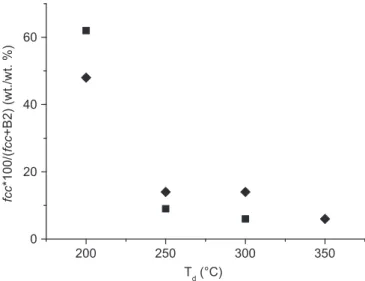
except for 350 1C, where it slightly increases to attend 25 at% for films processed under VUV activation.Fig. 4presents the fcc over the sum fcc plus B2 weight ratio of the Pd–Cu phases in the films as a function of Td. It can be noticed that the fcc phase prevails at
the lowest Td; i.e. for films processed at 200 1C. In this
tempera-ture, the considered ratio exceeds 60% for films processed under thermal activation, and it reaches almost 50% for those processed under VUV assistance. For both type of films, this ratio strongly
Fig. 4. fccover the sum fcc plus B2 weight ratio of the Pd–Cu phases in the films as a function of Td. Squares and diamonds correspond to films processed by thermal,
and combined thermal and VUV activation, respectively.
Fig. 5.SEM surface views for typical Pd–Cu alloy films prepared under thermal activation at Td¼250 1C (a) and 350 1C (c) and combined thermal plus VUV activation at
decreases with increasing Td to reach 14% and 9% for films
processed with and without VUV activation, respectively. Above this temperature it slightly decreases for both types of films.
Fig. 5presents SEM surface views of four samples, processed at
Td¼250 1C and 350 1C under thermal and combined thermal plus VUV activation. The estimated thickness of all films is between 200 nm and 300 nm. Films present a uniform microstructure, composed of grains which are facetted at Td¼250 1C indepen-dently of the activation mode. Grain size at this Td is
approxi-mately 70–80 nm, slightly less for films grown under VUV. Increase of Tdto 350 1C results in round shaped grains whose size
is ca. 150 nm for films grown under thermal activation. In contrast, the grain size of films grown at this Td under VUV does not
significantly increase. These films are more smoother and more compact; i.e. they present a reduced porosity than the thermally grown ones, independently of Td.
4. Conclusion
A novel approach for the preparation of Pd-alloy membrane materials by CVD is demonstrated. Pd–Cu films were deposited from PdL2CuL2,
(L¼2-methoxy-2,6,6-trimethylheptane-3,5-dio-nate), a new, non-toxic, halogen free single source bimetallic precursor with a 1:1 Cu/Pd ratio. Deposition conditions were 10 Torr, under thermal (temperature range 200–350 1C) and com-bined thermal and Vacuum Ultra Violet activation. Films of tunable composition and microstructure have been obtained in this para-metric space. They are composed of the cubic B2 and the fcc Pd–Cu phases, with predominance of the former and significant content of the latter at low deposition temperature. Films are system-atically Cu-rich, with a mean value of Cu/Pd ratio of 55/45. The morphology of the films is uniform and rough, with faceted grains for films deposited under thermal activation, the size of which increases from 70 to 80 nm at 250 1C to ca. 150 nm at 350 1C. These grains are composed of crystallites, whose size increases from 1075 nm at 200 1C to ca. 45 nm at 350 1C. VUV activation of the deposition results in higher growth rate and in a moderate increase of the carbon content of the films which passes from approximately 15 at% to 20 at% and even 25 at% at 350 1C. It also provides films with smoother morphology and a slightly higher content of the fcc phase in the temperature range 250–300 1C, namely ca. 17 wt% to be compared with 10 wt% and less for films deposited through thermal activation. Carbon impurities determi-nation seems to be problematic and needs further verification.
Acknowledgments
The authors are grateful to Mrs. T.P. Koretskaya (Nikolaev Institute of Inorganic Chemistry SB RAS) for VUV-assisted experiments, Dr. N.I. Petrova and Dr. A.R. Tsygankova (Nikolaev Institute of Inorganic Chemistry SB RAS) for ISP-AES analysis, Dr. E.V. Maximovskiy (Nikolaev Institute of Inorganic Chemistry SB RAS) for operating SEM, and Dr. V.V. Kaichev (Boreskov Institute of Catalysis SB RAS) for the help with XPS analysis. The reported study was partially supported by RFBR, research Project no. 14-03-00411-a.
References
[1]F. Gallucci, A. Basile, F. Ibney Hai, Introduction – a review of membrane reactors, in: A. Basile, F. Gallucci (Eds.), Membranes for Membrane Reactors: Preparation, Optimization and Selection, John Wiley & Sons, United Kingdom, 2011, pp. 1–61.
[2]G.S. Burkhanov, N.B. Gorina, N.B. Kolchugina, N.R. Roshan, D.I. Slovetsky, E.M. Chistov, Platin. Met. Rev. 55 (1) (2011) 3–12.
[3]G.Q. Lu, J.C. Diniz da Costa, M. Duke, S. Giessler, R. Socolow, R.H. Williams, T. Kreutz, J. Colloid Interface Sci. 314 (2007) 589–603.
[4]P.M. Thoen, F. Roa, J.D. Way, Desalination 193 (2006) 224–229.
[5]C. Resini, L. Arrighi, M.C. Herrera Delgado, M.A. Larrubia Vargas, L.J. Alemany, P. Riani, S. Berardinelli, R. Marazza, G. Busca, Int. J. Hydrog. Energy 31 (2006) 13–19.
[6]F. Borgognoni, S. Tosti, M. Vadrucci, A. Santucci, Int. J. Hydrog. Energy 38 (2013) 1430–1438.
[7]S. Tosti, Int. J. Hydrog. Energy 35 (2010) 12650–12659.
[8]Y. She, S.C. Emerson, N.J. Magdefrau, S.M. Opalka, C. Thibaud-Erkey, T.H. Vanderspurt, J. Membr. Sci. 452 (2014) 203–211.
[9]S. Nayebossadri, J. Speight, D. Book, J. Membr. Sci. 451 (2014) 216–225. [10]T.A. Peters, T. Kaleta, M. Stange, R. Bredesen, J. Membr. Sci. 383 (2011) 124–134. [11] R.J. Gouwen, C.J.G.M. de Kok, J.A.Z. Pieterse, Noble Metal Membrane Prepara-tion: Industrial Film Formation Techniques, CATO-2 Report # WP1.2.F1-D02. [12]J. Prabhuram, T.S. Zhao, Z.X. Liang, H. Yang, C.W. Wong, J. Electrochem. Soc. 152
(7) (2005) A1390–A1397.
[13]M.Z.F. Kamarudin, S.K. Kamarudin, M.S. Masdar, W.R.W. Daud, Int. J. Hydrog. Energy 38 (2013) 9438–9453.
[14]K. Babita, S. Sridhar, K.V. Raghavan, Int. J. Hydrog. Energy 36 (2011) 6671–6688.
[15]E. Antolini, E.R. Gonzalez, J. Power Sources 195 (2010) 3431–3450. [16]V. Bhaskaran, P. Atanasova, M.J. Hampden-Smith, T.T. Kodas, Chem. Mater. 9
(1997) 2822–2829.
[17] C.W. Park, R.W. Vook, Thin Solid Films 226 (1993) 238–241.
[18]C. Vahlas, Chemical vapor deposition of metals: from unary systems to complex metallic alloys, in: E. Belin-Ferré (Ed.), Complex Metallic Alloys: Surfaces and Coatings, World Scientific, Singapore, 2010, pp. 49–81. [19]B.M. Kuchumov, T.P. Koretskaya, Y.V. Shevtsov, S.V. Trubin, G.I. Zharkova,
V.S. Danilovich, I.K. Igumenov, V.N. Kruchinin, ECS Trans. 25 (8) (2009) 909–916.
[20] Powder Diffraction File, PDF-2/Release 2009, 2009: International Centre for Diffraction Date, USA.
[21] W. Kraus, G. Nolze, PowderCell 2.4, Program for the Representation and Manipulation of Crystal Structures and Calculation of the Resulting X-Ray Powder Patterns, Berlin, 2000.
[22] S. Krumm, Mater. Sci. Forum 183 (1996) 228–231.
[23] C.D. Wagner, W.M. Riggs, L.E. Davis, J.F. Moulder, Handbook of X-Ray Photo-electron Spectroscopy, in: G.E. Muilenberg (Ed.), Perkin-Elmer Corporation, Eden Prairie, Minnesota, USA, 1978.
[24] B. Predel, Cu–Pd (copper–palladium), in: O. Madelung (Ed.), SpringerMater-ials–The Landolt-Börnstein Database 〈http://www.springermaterials.com〉, doi: 10.1007/10086090_1102.
[25] W. Huang, S.M. Opalka, D. Wang, T.B. Flanagan, Thermodynamic modelling of the Cu–Pd–H system, CALPHAD 31 (2007) 315–329.
[26] M. Hansen, K. Anderko, Constitution of Binary Alloys, Mc Graw-Hill, New York (1958) 1305.
[27] J. Batista, A. Pintar, D. Mandrino, M. Jenko, V. Martin, Appl. Catal. A. 206 (2001) 113–124.
[28] Thomas Christiansen, A.J. Somers, Marcel, stress and composition of carbon stabilized expanded austenite on stainless steel, Metall. Mater. Trans. A Phys. Metall. Mater. Sci. 40A (8) (2009) 1791–1798.
[29] V.I. Bukhtiyarov, V.V. Kaichev, I.P. Prosvirin, Top. Catal. 32 (2005) 3–15. [30] N.S. McIntyre, M.G. Cook, Anal. Chem. 47 (1975) 2208–2213.
[31]J.C. Otamiri, S.L.T. Andersson, A. Andersson, Appl. Catal. 65 (1990) 159–174. [32] S. Poulston, P.M. Parlett, P. Stone, M. Bowker, Surf. Interface Anal. 24 (1996)
811–820.
[33] M. Richter, M.J.G. Fait, R. Eckelt, M. Scneider, J. Radnik, D. Heidemann, R. Fricke, J. Catal. 245 (2007) 11–24.
[34] B.R. Strohmeier, D.E. Leyden, R.S. Field, D.M. Hercules, J. Catal. 94 (1985) 514–530.
[35] S.A. Khromova, A.A. Smirnov, O.A. Bulavchenko, A.A. Saraev, V.V. Kaichev, S.I. Reshetnikov, V.A. Yakovlev, Appl. Catal. A 470 (2014) 261–270.
[36] T. Yano, M. Ebizuka, S. Shibata, M. Yamane, J. Electron Spectrosc. Relat. Phenom. 131–132 (2003) 133–144.