HAL Id: hal-02572398
https://hal.archives-ouvertes.fr/hal-02572398
Submitted on 13 May 2020
HAL is a multi-disciplinary open access
archive for the deposit and dissemination of
sci-entific research documents, whether they are
pub-lished or not. The documents may come from
teaching and research institutions in France or
abroad, or from public or private research centers.
L’archive ouverte pluridisciplinaire HAL, est
destinée au dépôt et à la diffusion de documents
scientifiques de niveau recherche, publiés ou non,
émanant des établissements d’enseignement et de
recherche français ou étrangers, des laboratoires
publics ou privés.
Experimental Analysis of the Electromagnetic
Instruction Skip Fault Model
Alexandre Menu, Jean-Max Dutertre, Olivier Potin, Jean-Baptiste Rigaud,
Jean-Luc Danger
To cite this version:
Alexandre Menu, Jean-Max Dutertre, Olivier Potin, Jean-Baptiste Rigaud, Jean-Luc Danger.
Ex-perimental Analysis of the Electromagnetic Instruction Skip Fault Model. 15th Design &
Tech-nology of Integrated Systems in Nanoscale Era (DTIS 2020), Apr 2020, Marrakech, Morocco.
�10.1109/DTIS48698.2020.9081261�. �hal-02572398�
Experimental Analysis of the Electromagnetic
Instruction Skip Fault Model
Alexandre Menu
∗, Jean-Max Dutertre
∗, Olivier Potin
∗, Jean-Baptiste Rigaud
∗,
Jean-Luc Danger
†∗Mines Saint-Etienne, CEA-Tech, Centre CMP, F - 13541 Gardanne France
{dutertre, alexandre.menu, rigaud, potin}@emse.fr
†LTCI, T´el´ecom Paris, IP Paris, France
Abstract—Microcontrollers storing valuable data or using se-curity functions are vulnerable to fault injection attacks. Among the various types of faults, instruction skips induced at runtime proved to be effective against identification routines or encryption algorithms. Until recently, most research works assessed a fault model that consists in a single instruction skip, i.e. the ability to prevent one chosen instruction in a program from being executed. We question this fault model for EM fault injection on experimental basis and report the possibility to induce several consecutive instructions skips.
Index Terms—EM fault injection, fault model
I. INTRODUCTION
Hardware attacks take advantage of the physical implemen-tation of an electronic device to overcome its security features. To this purpose, either passive side channel techniques or active fault injection techniques can be used. The former is out of the scope of this article. Fault injection techniques aims to force the device out of its specification by altering its environmental conditions [1] (e.g. its voltage, temperature, frequency, etc.). An attacker that successfully induces an erroneous behavior refers to it as an injected fault. These faults can then be used as an attack primitive to extract a cryptographic key [2] or provide an unauthorized access to some of the target functionalities [3]. The set of properties of a fault induced by an electromagnetic (EM) pertubartion (or by any other fault injection means) is referred to as a fault model (FM). It is often linked to a given attack scheme and expressed as an ability to meet requirements in terms of synchronization with the target activity and extension of the induced fault (e.g. the FM of the well-known Piret fault attack (FA) [4] requires to fault one byte of the AESalgorithm calculations before its last MixColumn transformation).
Among fault injection (FI) techniques, laserFIandEMfault injection (EMFI) achieve the best performances [5]–[7]. Laser is probably the most expensive FImeans, however it makes it possible to inject faults with high accuracy even at advanced technology nodes [5]. It is accurate both in terms of timing (faults may be injected with laser pulses as short as a few picoseconds [8]) and in terms of location (its effect is mainly limited to the logic gate located within its spot size which
This research has been partially supported by the European Commission under H2020 SPARTA (Grant Agreement 830892).
may be as low as a few micrometers [6]). EMFI on the other hand does not require a direct access to the die, the clock, or the power supply of the target, while enabling an attacker to fault micro-architectural features [9]. As an operational setup can be build for less than a thousand dollars [10], EMFI is currently the best compromise between price and locality.
In this work, we report our analysis of the EM-induced instruction skipFM. ThisFMrelates to how a given instruction of a microcontroller program may be skipped (i.e. not exe-cuted) at runtime. Several works already described thisFMand assessed the possibility ofEM-induced single instruction skips [11]–[14]. The assessment of FMs on experimental grounds is of high interest regarding how FIs countermeasures (CMs) are designed and tailored. As a matter of example, the authors of [14] discussed two CMs based on instruction redundancy designed on the assumption that an attacker is only able to induce single instruction skips. Would this assumption be proved wrong, theirCMs would be vulnerable.
Our experiments extend further this FM by reporting the feasibility of inducing several successive instructions skips by
EM perturbation.
Our contributions are as follows:
• We achieve to skip, with a perfect reproducibility, several consecutive fetch operation with a single pulse, controling both the timing and the number of affected instructions,
• We highlight the influence of the width of the voltage pulse on the observed fault model,
• We demonstrate practical application on an 8-bit
micro-controller, bypassing state-of-the-art softwareCM. This article is organized as follows. Section II discusses the state-of-the-art of instruction skips and introduces the aim of our work. Our experimental setup and settings are described in section III. Section IV reports the obtained results. Then, the assessed FM is discussed in section V. Section VI concludes the paper.
II. THEEM-INDUCED INSTRUCTION SKIP FAULT MODEL
Our research objective was to reproduce EM-induced in-struction skips on a microcontroller and study the main characteristics of its FM: accuracy, extent, success rate, etc. Our aim was also to assess if the multiple instructions skip fault model relies on specific micro-architectural features (i.e.
Authors’ version
https://doi.org/10.1109/DTIS48698.2020.9081261
Design Technology of Integrated Systems In Nanoscale Era (DTIS),
2020 15th IEEE International Conference On
cache or pipeline). This question is paramount, as CMs based on a too narrow FM may reveal vulnerabilities at test time. A. Fault model definition
A fault model refers indisctintly either to the abstract properties of a fault or to the main properties of aFAscheme. These are often expressed in terms of extension (e.g. bit, byte, nibble) and synchronization with the execution of the program. However, a fault and a FA scheme are most conveniently described at two different level of abstraction, i.e. the physical layer and the logical layer. The authors of [5] follow the former approach and describe laser-induced set and bit-reset faults at the transistor and gate level. However, this approach is extremely difficult and time consuming if the attacker has a limited insight on the device internals. The authors of [4] follow the latter approach and describe a mono-byte FM to corrupt the AES algorithm calculations before its last MixColumn transformation. However, this approach faces practical limitations in understanding the underlying fault mechanism because of the complex interaction between the physical and the logical layer of an electronic device.
The instruction set architecture (ISA) is a natural interface between the physical and the logical layer. Previous work highlighted that the charaterization of FM at the level of the
ISAcovers a wide range of practical faults [14], [15]. In this article, we followed this approach and analyzed the behavior of microcontrollers at the level of the ISA in order to assess
EM-induced instruction skips. B. Instruction skip fault model
An instruction skip is a fault that results in skipping, mean-ing not executmean-ing, one instruction of a program at runtime. There is to date very few explanations of how an instruction skip is induced at gate level, with the notable exception of [15]. It describes how progressively increasing the stress applied by a clock glitch to a microcontroller induces an increasing number of bit-reset faults into the opcode of an instruction. It results in (1) instruction modification at low stress or (2) in turning the instruction into an actual no operation instruction (nop) at high stress.
An instruction modification has the same effect as an instruction skip if the modified instruction has no effect on the context of the program. While this modification are the most frequent in practice [16], we focused our experiments toward achieving instruction skips by turning the target instructions into nop instructions.
Several works studied the EM-induced instruction skip FM. Most of them assessed single instruction skips, in the same 8-bit microcontroller as the one studied in this work [11], in a 32-bit microcontroller [14], and in an FPGA based RISCV implementation [17].
Several works also studied the laser-induced instruction skip
FM. In [18], the authors obtained single instruction skips with high accuracy and high success rate. Still on the same target, [19] reports single instruction skips based on resetting one or two bits of the targeted instruction opcode. The authors of
[20] induced single instruction skips on a more complex 32-bit cortex-M3 microcontroller. They were able to inject two single instruction skips distant from 58 ms to defeat a protected CRT-RSA algorithm.
While the instruction skip FM alone does not encompass the complexity of practical faults [16], skipping multiple instructions was, until recently, a theoritical consideration. C. Multiple instructions skip fault model
The state-of-the-art in laser-induced instruction skip reports that the number of successive instructions that could be skipped was not limited in the same 8-bit microcontroller as the one studied in this work [21]. Moreover, the injection can be syncronized with the program execution and the duration of the laser pulse is linearly correlated with the number of consecutive instructions which are skipped. This is a strong
FM as entire sections of code can be selectively erased by an attacker. To the best of our knowledge, the only works reporting several successive instructions skips with other in-jection techniques are [9], [22] and [23]. The authors of [9] assessed four successive EM-induced skips of instructions stored in the instruction cache of an ARMv7 microcontroller. The authors of [22] succeeded in faulting instructions stored in the pipeline of a FPGAimplementation of the LEON7 core with a clock glitch. Last but not least, the authors of [23] reportedEM-induced skips of up to six consecutive instructions with a low repeatability on a RISC-V FPGA implementation. However, they did not provide an understanding of the micro-architectural effects.
Based on previous experiments and taking into account the state-of-the-art we described, we focused our experiments toward achieving instruction skips by turning the targeted instructions into nop instructions. Our experiments were car-ried out with the same 8-bit microcontroller studied by [11], [15], [18], [19], so that our results can be easily compared. Moreover, this microcontroller has a very simple 2-stage pipelined architecture and no caches, which is easy to analyse in the absence of unwanted architectural effects. The results of this research should give a better insight on the tradeoff between the laser and theEMinjection techniques on the basis of the instruction skip FM.
III. EXPERIMENTAL SETTINGS
A. EM injection bench
The EMpulse injection setup we used is similar to the one described in [7], it consists in the following elements:
• a voltage pulse generator,
• an injection probe,
• a XYZ positioning table,
• an oscilloscope,
• a target (described in III-B),
• a control PC interfacing the different elements of the bench and running the test series.
TheEMdisturbance that induces a fault is generated thanks to the voltage pulse generator: it delivers a square voltage pulse with a transition time of 2 ns (for the first edge of the pulse,
Fig. 1. Frontside view of the ATmega328P test chip - Flash, RAM and
EEPROMmemories highlighted in red; fault sensitive areas for laser andEM
injection highlighted resp. by a small and a greater deep blue stars.
the second edge has a transition time of 5 ns), a maximum amplitude of ±400 V, and a width in the 6 - 100 ns range. The voltage pulse edges are converted into current variations in a coil wrapped arround the tip of a handcrafted injection probe. The coil is made of six turns of copper wire around a ferrite core which diameter is ∼ 500µm. The swift current variation induces an EMperturbation at the root cause of the injected faults. A trigger signal generated by the device under test synchronizes the voltage pulse with the operation of the microcontroller target.
B. Test chip
We chose a simple target for the purpose of being able to analyse easily its responses to fault injection: an 8-bit non-secure ATmega328P microcontroller designed in the old
CMOS 0.35 µm technology. It has 2 kB RAM, 3 kB Flash and 1 kBEEPROMmemories; a Harvard architecture with a 2-stage fetch-execute pipeline. It runs at 16 MHz and has 32 general purpose registers (registers r16 to r25 were used during our experiments). Figure 1 gives a front view of the test chip with its Flash, RAM and EEPROM memories highlighted in red. The laser sensitive area that makes it possible to induce an instruction skip is highlighted by a small deep blue star (slightly outside the Flash memory at its left), it is in the order of a few micrometers [21]. TheEMsensitive area, which is convenient for inducing instruction skips, is larger (see experimental results in section IV), it is in the order of a hundred of micrometers. It is located in the bottom-right part of the Flash memory and highlighted by a greater deep blue star in Fig. 1. As the strength of the magnetic field generated by the coil strongly decreases with the distance from the injection probe, it was placed close to the target’s silicon die (∼1 mm). To this end, the package of the target device was open on its top by chemical etching.
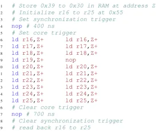
1 # Store 0x39 to 0x30 in RAM at address Z
2 # Initialize r16 to r25 at 0x55 3 # Set synchronization trigger
4 nop # 400 ns 5 # Set core trigger
6 ld r16,Z+ ld r16,Z+ 7 ld r17,Z+ ld r17,Z+ 8 ld r18,Z+ ld r18,Z+ 9 ld r19,Z+ nop 10 ld r20,Z+ ld r20,Z+ 11 ld r21,Z+ ld r21,Z+ 12 ld r22,Z+ ld r22,Z+ 13 ld r23,Z+ ld r23,Z+ 14 ld r24,Z+ ld r24,Z+ 15 ld r25,Z+ ld r25,Z+
16 # Clear core trigger
17 nop # 700 ns
18 # Clear synchronization trigger
19 # read back r16 to r25
Listing 1: Test code - Instruction skip analysis.
C. Test codes
We studied the effect ofEM-induced faults on dedicated test codes mostly written in assembly langage. Our intent was to induce and analyze instruction skips by examining their effect. For each test series, we used two trigger signals for syn-chronization purposes (two outputs of the test chip):
• a synchronization trigger signal to accommodate for the
latency of ourEM injection setup (about ∼ 300 ns),
• a core trigger signal to synchronize the actualEM pertur-bation (thanks to an image of the transmitted perturba-tion) with the part of the assembly code of interest. Listing 1 provides a description of the test code we used to tune our settings in order to induce instruction skips. The core part of the test code (encompassed by the core trigger setting and clearing) is a series of ten ld rX,Z+ instructions. Each one corresponds to a load in a destination register rX of a byte value stored in RAM memory at address Z with a post increment of Z. Prior to that, the ten destination registers, r16 to r25, are initialized at 0x55 and an array of ten byte values 0x39to 0x30 are stored inRAM with Z storing the address of its first element. Registers r16 to r25 are read back after the synchronization trigger is reseted. The two top signals in Figure 2 are the synchronization and core triggers, the bottom blue signal is an approximated image of the EM perturbation (obtained by wrapping the wire end of a coaxial line around the wire conducting the voltage pulse to the injection probe). The top part of Table I displays the values read back from r16to r25 for a fault-free execution.
TABLE I
REGISTERS R16TO R25READ BACK VALUES,FOR A FAULT FREE EXECUTION(TOP)AND FOR AN INSTRUCTION SKIP(BOTTOM).
Register 16 17 18 19 20 21 22 23 24 25 Fault free 0x39 0x38 0x37 0x36 0x35 0x34 0x33 0x32 0x31 0x30 Register 16 17 18 19 20 21 22 23 24 25
Faulted 0x39 0x38 0x37 0x55 0x36 0x35 0x34 0x33 0x32 0x31 As an example, the right column of the test code core part in listing 1 displays the effect of an EM perturbation turning
EM perturbation Vpulse: -200 V / 100 ns With EM perturbation 0 10-6 2.10-6 3.10-6 4.10-6 [s] 0 V 5 V 0 V 5 V 0 V Normal operation 1xTclk Synchronization trigger Core trigger
Fig. 2. EM-induced single instruction skip: effect on execution time, triggers waveforms modification due to EMinjection (from top to bottom, synchro-nization trigger, core trigger, and approximated image of theEMperturbation).
the ld instruction of line 9 into a nop instruction. The effect of such an EM-induced instruction skip is highlighted in the bottom part of table I: the initialization value 0x55 is read back from r19 (in red), and because an increment of address Z is missing, all the values read back from r20 to r25 are shifted (in black).
IV. EXPERIMENTAL RESULTS
A. Finding the Points-of-Interest
EMFIhas a local effect ( [7], [24]) that may be classified in between the strongly local effect of laserFI[21] and the global effect of otherFImeans (such as clock and power glitches). As a result, the position of the injection probe w.r.t. the target has a significant effect on the FIprocess: a fault may be injected
or not, different FMs may be obtained ( [7], [11], [12]). Our research objective was to induce instruction skips similar to that described in [21] for laser FI. This implied to test a large amount of settings: injection probe location, synchronization with the test code, and voltage pulse parameters. Because this search space has several dimensions, this process could be very time consuming, especially regarding the XY position of the injection probe (for the other parameters, previous work helped us to converge in a matter of a few hours). It took approximately a week to find the right settings allowing to induce an instruction skip (the injection probe location is shown in Fig. 1).
Figure 2 exemplifies the kind of instruction skip that can be observed. It displays the trigger signals of the test code (two top waveforms) and an image of the EM perturbation (third waveform). The trigger signals are both drawn for a fault-free execution (in red, denoted as ’normal operation’) and for anEM-injection that induces an instruction skip of the ld instruction into register r19 (in blue). Because execution of a ld instruction takes two clock periods contrary to that of a nop instruction which takes one clock period, each consecutive instructions skip shall correspond to a reduction of the test code of one clock period. This phenomenon is displayed in Fig. 2. The test code execution time is shortened
r19
~25nsr16
r25
Fig. 3. EM-induced single instruction skip: ability to choose the skipped instruction - Faulted registers as a function ofEMinjection time (ns) for a −200 V voltage amplitude and 100 ns pulse width.
as well as the duration of the triggers signals: the faulted execution triggers in blue last one clock period less than the fault free execution. This experiment was performed with a voltage pulse amplitude set to −200 V and a width of 100 ns (the values read back from the registers were actually those mentioned in the bottom part of Table I). For these settings a 100 % success rate was achieved.
It assessed the ability ofEMFIto induce an instruction skip in a running microcontroller. These settings (in particular the injection probe location) served as a basis for the experiments we carried out to analyze further the EM instruction skip FM
(as reported in the following subsections). B. EM-induced instruction skip, test of accuracy
In terms of accuracy, we tested whether the single in-struction skip fault model was still valid while targeting the ld instruction of the other test registers. Our aim was to assess an attacker ability to target an arbitrary instruction in a program. To do so, we sweeped the time delay between the
EM-perturbation and the synchronization trigger signal to span the whole test code. Figure 3 reports the obtained results. It displays the skipped registers (positions 1 to 10 correspond to registers r19 to r25) as a function of the delay. It reveals that an attacker is able to injectEM-induced single instruction skips into a running microcontroller with high timing accuracy. For each instruction, we were indeed able to find an injection timing leading to a 100 % success rate.
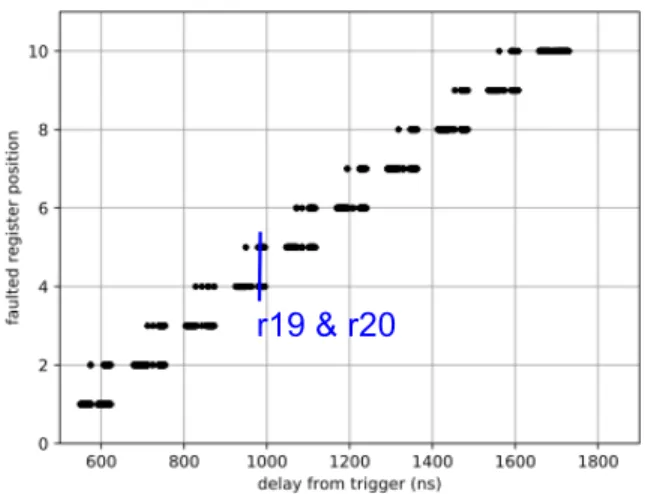
C. EM-induced multiple instructions skip
Some experimental results (not reported here) suggested that several consecutive instructions may be skipped simul-taneously. In order to verify this assumption, we again carried out our experiments with a voltage pulse amplitude increased to -250 V. The corresponding results are displayed in Fig. 4. It shows that this increase makes it possible to skip two consecutive instructions with a still high timing accuracy (i.e. the ability to choose the two instructions that are skipped). As
r19 & r20
Fig. 4. EM-induced instruction skip: ability to skip two consecutive instruc-tions - Faulted registers as a function of EM injection time (ns) (−250 V voltage amplitude and 100 ns pulse width).
an illustration (denoted in blue in Fig. 4), the two successive load instructions into r19 and r20 are skipped for a trigger to shot delay of 980 ns. A further increase of the voltage pulse amplitude to −400 V did not change the number of skips (similar results were obtained using positive voltage pulses).
In addition, we discovered that tuning the width of the voltage pulse had an effect on the number of achievable successive skips. The use of different values of the voltage pulse width leaded to different number of skips as reported in Fig. 5. For the same settings (location, voltage amplitude, and delay) but different pulse widths, up to four successive instructions skips were obtained (for a width between 20 ns and 35 ns). The tuning of the width also made it possible to choose precisely the number of skips: 2, 3 or 4. With other settings (location and voltage amplitude) we ascertained the ability to increase to six the number of successive instructions skipped.
Voltage pulse width [ns]
Fig. 5. EMinduced instruction skip: effect of the voltage pulse width -Number of EM-induced instruction skips as a function of the voltage pulse width (ns).
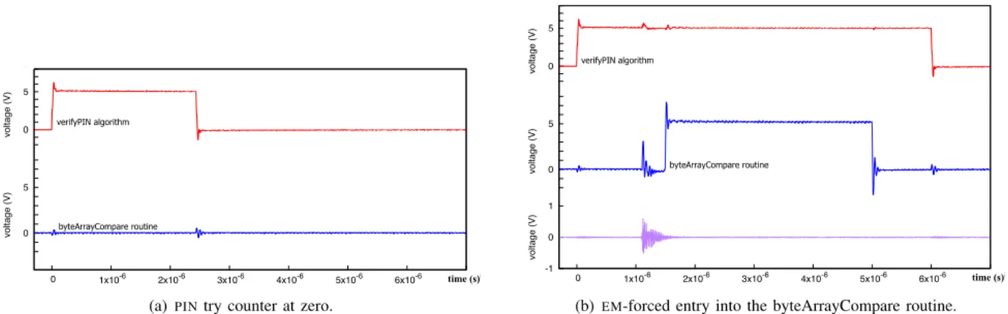
D. PIN bypass withEMperturbation
In order to improve our assessment of the threat raised by EM-induced instruction skips, we targeted a 4-digit PIN
verification algorithm (described in [3] and denoted by verifyPIN hereafter). It is protected against brute force attacks (i.e. attacks that consist in testing all existing PIN
codes) thanks to a trial counter (denoted by g_ptc hereafter). The value of the counter is tested before calling the PIN
verification routine: byteArrayCompare (it is in charge of comparing the user PIN to a reference PIN). g_ptc is decremented and memorized before each verification. It is initialized at 3 (and restored to this value after a success-ful identification). If g_ptc reaches zero, a conditional if statement denies the entry into the byteArrayCompare routine. As a result, the verification systematically fails. The (simplified) pseudo-code of this algorithm is shown in Listing 2, where BOOL_TRUE and BOOL_FALSE are resp. the true and false boolean values, and g_auth a variable indicating whether the user is authenticated or not (g_auth set to BOOL_TRUE indicates that the user has been successfully authenticated).
1 BOOL g_auth = BOOL_FALSE;
2 ... 3 g_ptc--; 4 if(g_ptc > 0){ 5 if(byteArrayCompare(...) == 1){ 6 g_ptc = 3; 7 g_auth = BOOL_TRUE; 8 } 9 }
Listing 2: C code of the verifyPIN algorithm.
[3] describes several instruction skip attacks that may result in a successful PIN bypass: most of them targeting one or a few successive code instructions. We chose to implement that which consists in skipping the verification of the trial counter (line 4 of Listing 2), allowing us to perform a bruteforce attack on the four digits of the secret PINcode.
Figure 6 displays the trigger signals highlighting the ex-ecution of the verifyPIN algorithm in red, and of the byteArrayCompare routine in blue. When g_ptc equals zero (Fig. 6.a), the access to the byteArrayCompare routine is denied (the corresponding trigger stays low). Fig. 6.b reports a successful EMFI attack (an image of the EM per-turbation is depicted in purple) that forces the entry into the byteArrayCompare routine: the PIN code entered by the attacker is checked against the reference PIN despite the exhaustion of thePINtry counter. We were able to find settings that achieve a 100% success rate and then to brute force the verifyPINalgorithm.
V. DISCUSSION
A. EM-induced instruction skip fault model
The experimental results reported in section IV demonstrate that a very high accuracy is achievable with EM-induced instruction skips: we were able to choose and skip a single
Verify pin authentication locked trigger -2 -1 0 1 2 3 4 5 6 7 8 voltage (V) -2 -1 0 1 2 3 4 5 6 7 8 0 1x10⁻⁶ 2x10⁻⁶ 3x10⁻⁶ 4x10⁻⁶ 5x10⁻⁶ 6x10⁻⁶ 7x10⁻⁶ voltage (V) time (s) time (s) verifyPIN algorithm byteArrayCompare routine
(a)PINtry counter at zero.
Verify pin locked authentication skip
-2 -1 0 1 2 3 4 5 6 7 8 voltage (V) -2 -1 0 1 2 3 4 5 6 7 8 voltage (V) -1 0 1 0 1x10⁻⁶ 2x10⁻⁶ 3x10⁻⁶ 4x10⁻⁶ 5x10⁻⁶ 6x10⁻⁶ 7x10⁻⁶ voltage (V) time (s) time (s) verifyPIN algorithm byteArrayCompare routine
(b)EM-forced entry into the byteArrayCompare routine. Fig. 6. Illustration ofPINbypass throughEM-induced instruction skip.
instruction of a test sequence with a 100 % success rate. Moreover, we were able to increase its extent to skip six successive instructions which adds to its strengh (unlike [9], [22], the ability to skip consecutive instructions was not linked to the micro-architecture of the target). From an at-tacker perspective, this attack does not require any insight on the underlying micro-architecture, which makes it easily reproducible. This FM has been successfully applied to brute force a PINverification algorithm. We demonstrate on a 8-bit microcrontroller that several consecutive fetch operation can be skipped with a single EMpulse, extending the currentFMs. This fault model shares similarities with laser-induced in-struction skips in terms of accuracy and repeatability under the same synchronization requirements. However, the number of consecutive instructions which can be skipped is limited with theEMinjection technique, whereas an arbitrary number of instruction can be blinded with laser injection [21]. This difference might be understood as a difference in the nature of the stress induced by laser andEMinjection techniques. The former can be precisely tuned with the laser power and pulse duration, whereas the latter only occurs during the rising edge of the EM pulse. While software CMs against EM-injection may take advantage of this temporal limitation, the number of consecutive instructions which can be skipped might be higher than the number assessed in this article.
Finally, we underline the importance of synchronization of the EM injection with the target code to achieve the high repeatability we report. We also refer the reader to [21] for a discussion on how synchronization may be obtained.
B. Discussion of the EM-induced fault injection mechanism Several physical mechanisms have been proposed to de-scribe the faults induced by an EM pulse [7], [13], [25]. The authors of [7] and [13] highlighted the similarities between
EM induced faults in an IC and faults that were obtained with the violation of timing constraints. A model of the glitch induced by an EMpulse on a power-ground network was later proposed in [26]. The authors of [25] suggested that glitching the set and reset circuitry corrupts the operation of D-flip-flop memory cells, thus explaining the specificity of the timing of
EMinjections. In the same time, the authors of [27] measured and analyzed the effets of an EMpulse on the clock circuitry of a FPGA. The diversity of suggested hypothesis reflects the complexity of the analysis of EMphysical effects.
In this article, we observed a non-linear correlation between the width of theEMpulse and the number of skipped instruc-tions. This result shares some similarities with [28], where damped oscillation where obtain by glitching a FPGA power supply with a voltage pulse. The authors observed constructive and destructive interference for various duration of the pulse. Moreover, positive and negative polarities of the voltage pulse were shown to have the same effects, as this is the case with our experiments. These elements support the hypothesis that we observed violation of timing constraints in our experiments.
VI. CONCLUSION
This research work assesses on experimental basis an ex-tended fault model forEM-induced instruction skips. The main characteristics of this fault model are:
• its accuracy, or ability to choose the skipped instruction with a 100 % success rate provided a precise synchro-nization is obtained,
• its extension, or ability to skip up to six successive instructions (without the help of any micro-architectural effect).
We also highlighted the influence of the width of the voltage pulse, which has been underestimated until now, in the properties of EM-induced faults.
Simply put, EMFI may offer an attacker the ability to erase a small part of several instructions of a microcontroller firmware at runtime. Though, this EM fault model is not as threatening as the laser FM that offers the ability to erase
several chosen parts of arbitrary length of a running program [21]. It nonetheless extends the threat model that shall be considered when securing microcontrollers against FAs as
EMFI is more common and affordable than laserFI. ACKNOWLEDGMENT
This research has been partially supported by the European Commission under H2020 SPARTA (Grant Ag. 830892).
REFERENCES
[1] A. Barenghi, L. Breveglieri, I. Koren, and D. Naccache, “Fault injection attacks on cryptographic devices: Theory, practice, and countermea-sures,” Proceedings of the IEEE, vol. 100, pp. 3056 – 3076, 2012. [2] D. Boneh, R. A. DeMillo, and R. J. Lipton, “On the importance
of checking cryptographic protocols for faults,” in Advances in Cryptology, International Conference on the Theory and Application of Cryptographic Techniques, 1997.
[3] L. Dureuil, G. Petiot, M.-L. Potet, T.-H. Le, A. Crohen, and P. de Choudens, “FISSC: A fault injection and simulation secure collection,” in International Conference on Computer Safety, Reliability, and Security, 2016.
[4] G. Piret and J.-J. Quisquater, “A differential fault attack technique against SPN structures, with application to the AES and Khazad,” in Cryptographic Hardware and Embedded Systems, Berlin, Heidelberg, 2003.
[5] J.-M. Dutertre, V. Beroulle, P. Candelier, S. De Castro, L.-B. Faber, M.-L. Flottes, P. Gendrier, D. H´ely, R. Leveugle, P. Maistri, G. Di Natale, A. Papadimitriou, and B. Rouzeyre, “Laser fault injection at the CMOS 28 nm technology node: an analysis of the fault model,,” in 2018 Workshop on Fault Diagnosis and Tolerance in Cryptography, 2018. [6] S. Buchner, F. Miller, V. Pouget, and D. McMorrow, “Pulsed-laser
testing for single-event effects investigations,” Nuclear Science, IEEE Transactions on, vol. 60, no. 3, pp. 1852–1875, June 2013.
[7] A. Dehbaoui, J.-M. Dutertre, B. Robisson, and A. Tria, “Electromagnetic transient faults injection on a hardware and a software implemen-tations of AES,” in Workshop on Fault Diagnosis and Tolerance in Cryptography, G. Bertoni and B. Gierlichs, Eds. Leuven, Belgium: IEEE Computer Society, 2012, pp. 7–15.
[8] M. Lacruche, N. Borrel, C. Champeix, C. Roscian, A. Sarafianos, J.-B. Rigaud, J.-M. Dutertre, and E. Kussener, “Laser fault injection into SRAM cells: Picosecond versus nanosecond pulses,” in On-Line Testing Symposium, 2015.
[9] L. Rivi`ere, Z. Najm, P. Rauzy, J.-L. Danger, and J. Bringer, “High preci-sion fault attacks on the instruction cache of ARMv7-M architectures,” in 2015 IEEE International Symposium on Hardware Oriented Security and Trust, 2015.
[10] A. Cui and R. Housley, “BADFET: Defeating modern secure boot using second-order pulsed electromagnetic fault injection,” in USENIX Workshop on Offensive Technologies (WOOT 17). Vancouver, BC: USENIX Association, Aug. 2017. [On-line]. Available: https://www.usenix.org/conference/woot17/workshop-program/presentation/cui
[11] A. Beckers, J. Balasch, B. Gierlichs, I. Verbauwhede, S. Osuka, M. Kinugawa, D. Fujimoto, and Y. Hayashi, “Characterization of EM faults on ATmega328P,” in International Symposium on Electromagnetic Compatibility. IEEE, 2019.
[12] N. Moro, A. Dehbaoui, K. Heydemann, B. Robisson, and E. Encrenaz, “Electromagnetic fault injection: Towards a fault model on a 32-bit microcontroller,” in Workshop on Fault Diagnosis and Tolerance in Cryptography, W. Fischer and J.-M. Schmidt, Eds. Los Alamitos, California, USA: IEEE Computer Society, 2013, pp. 77–88.
[13] N. Moro, K. Heydemann, E. Encrenaz, and B. Robisson, “Formal veri-fication of a software countermeasure against instruction skip attacks,” Journal of Cryptographic Engineering, vol. 4, no. 3, pp. 145–156, 2014. [14] N. Moro, K. Heydemann, A. Dehbaoui, B. Robisson, and E. Encrenaz, “Experimental evaluation of two software countermeasures against fault attacks,” in Hardware-Oriented Security and Trust, 2014.
[15] J. Balasch, B. Gierlichs, and I. Verbauwhede, “An in-depth and black-box characterization of the effects of clock glitches on 8-bit MCUs,” in Fault Diagnosis and Tolerance in Cryptography, 2011.
[16] L. Cojocar, K. Papagiannopoulos, and N. Timmers, “Instruction du-plication: Leaky and not too fault-tolerant!” in Smart Card Research and Advanced Applications, ser. Lecture Notes in Computer Science, T. Eisenbarth and Y. Teglia, Eds., vol. 10728. Springer, 2017, pp. 160–179.
[17] J. Proy, K. Heydemann, F. Maj´eric, A. Cohen, and A. Berzati, “Studying EM pulse effects on superscalar microarchitectures at ISA level,” CoRR, vol. abs/1903.02623, 2019. [Online]. Available: http://arxiv.org/abs/1903.02623
[18] J. Breier, D. Jap, and C.-N. Chen, “Laser profiling for the back-side fault attacks: With a practical laser skip instruction attack on AES,”
in Proceedings of the 1st ACM Workshop on Cyber-Physical System Security, New York, NY, USA, 2015.
[19] D. Kumar, A. Beckers, J. Balasch, B. Gierlichs, and I. Verbauwhede, “An in-depth and black-box characterization of the effects of laser pulses on ATmega328P,” in Smart Card Research and Advanced Applications, 2018.
[20] E. Trichina and R. Korkikyan, “Multi fault laser attacks on protected CRT-RSA,” in Fault Diagnosis and Tolerance in Cryptography, 2010. [21] J.-M. Dutertre, T. Riom, O. Potin, and J.-B. Rigaud, “Experimental
analysis of the laser-induced instruction skip fault model,” in The 24th Nordic Conference on Secure IT Systems, Nordsec 2019, A. Askarov, R. R. Hansen, and W. Rafnsson, Eds. Cham: Springer International Publishing, 2019, pp. 221–237.
[22] B. Yuce, N. F. Ghalaty, H. Santapuri, C. Deshpande, C. Patrick, and P. Schaumont, “Software fault resistance is futile: Effective single-glitch attacks,” in 2016 Workshop on Fault Diagnosis and Tolerance in Cryptography, 2016.
[23] M. Ehlmor, “Embedded systems security: On em fault injection on risc-v and br/tbr puf design on fpga,” Master’s thesis, University of Waterloo, Waterloo, Canada, 2020.
[24] L. Zussa, A. Dehbaoui, K. Tobich, J.-M. Dutertre, P. Maurine, L. Guillaume-Sage, J. Cl´ediere, and A. Tria, “Efficiency of a glitch detector against electromagnetic fault injection,” in Design, Automation and Test in Europe Conference and Exhibition (DATE), 2014, March 2014, pp. 1–6.
[25] S. Ordas, L. Guillaume-Sage, and P. Maurine, “Electromagnetic fault injection: the curse of flip-flops,” Journal of Cryptographic Engineering, vol. 7, no. 3, pp. 183–197, 2017.
[26] M. Dumont, P. Maurine, and M. Lisart, “Electromagnetic fault injection: how faults occur,” in 2019 Workshop on Fault Diagnosis and Tolerance in Cryptography (FDTC), ser. 15th Workshop on Fault Diagnosis and Tolerance in Cryptography, 2019.
[27] M. Ghodrati, B. Yuce, S. Gujar, C. Deshpande, L. Nazhandali, and P. Schaumont, “Inducing local timing fault through em injection,” in Proceedings - Design Automation Conference, ser. DAC ’18, vol. Part F137710. San Francisco, CA, USA: ACM, 2018, pp. 142:1–142:6. [28] L. Zussa, J.-M. Dutertre, J. Cl´ediere, and B. Robisson, “Analysis of the
fault injection mechanism related to negative and positive power supply glitches using an on-chip voltmeter,” in Hardware-Oriented Security and Trust (HOST), 2014 IEEE International Symposium on, 2014.