UNIVERSITÉ DE MONTRÉAL
MÉCANISMES PHYSIQUES ET FONDEMENTS THÉORIQUES DE LA RÉCUPÉRATION D’ÉNERGIE MICRO-ONDES AMBIANTE POUR LES DISPOSITIFS SANS FIL À FAIBLE
CONSOMMATION
CARLOS HENRIQUE PETZL LORENZ DÉPARTEMENT DE GÉNIE ÉLECTRIQUE ÉCOLE POLYTECHNIQUE DE MONTRÉAL
MÉMOIRE PRÉSENTÉ EN VUE DE L’OBTENTION DU DIPLÔME DE MAÎTRISE ÈS SCIENCES APPLIQUÉES
(GÉNIE ÉLECTRIQUE) DÉCEMBRE 2015
UNIVERSITÉ DE MONTRÉAL
ÉCOLE POLYTECHNIQUE DE MONTRÉAL
Ce mémoire intitulé :
MÉCANISMES PHYSIQUES ET FONDEMENTS THÉORIQUES DE LA RÉCUPÉRATION D’ÉNERGIE MICRO-ONDES AMBIANTE POUR LES DISPOSITIFS SANS FIL À FAIBLE
CONSOMMATION
présenté par : PETZL LORENZ Carlos Henrique
en vue de l’obtention du diplôme de : Maîtrise ès Sciences Appliquées a été dûment accepté par le jury d’examen constitué de :
M. LAURIN Jean-Jacques, Ph. D., président
M. WU Ke, Ph. D., membre et directeur de recherche M. CONSTANTIN Nicolas, Ph. D., membre
DÉDICACE
À mon épouse Antonia Yume Eiri Trebien Lorenz, qui m’a appuyé inconditionnellement pendant la maîtrise,
à mes parents Curt et Cristina Lorenz, qui m’ont enseigné l’importance de persévérer et de me dévouer au travail, mais aussi de garder du temps pour la famille et les amis,
à Simon Hemour pour m’avoir guidé pendant ce travail de recherche et pour toujours avoir été présent pour discuter de nouvelles idées.
REMERCIEMENTS
Je tiens à remercier en premier lieu à Dieu pour toutes ses bénédictions qu’il m’a offertes. Je tiens aussi à exprimer mes remerciements sincères à mon directeur de recherche, professeur Ke Wu, par son soutien et ses conseils donnés au cours de mes travaux de recherches; aussi comme par son soutien lors de mes moments de doute.
Un gros merci à Simon Hemour, qui était toujours présent pour discuter de nouvelles idées et méthodes pour résoudre les problèmes auxquelles j’ai fait face. Je suis certain que sans ton aide ce travail ne serait pas arrivé si loin.
Je voulais aussi remercier à tous les membres de l’équipe technique de Poly GRAMES, par leur soutien dans les fabrication et caractérisation des prototypes, aussi bien que par leur support informatique, à savoir Jules Gauthier, Traian Antonescu, Maxime Thibault, Steve Dubé et Jean-Sébastien Décarie. Je tiens aussi à remercier à Nathalie Levesque de l'École Polytechnique qui m’a toujours aidé lorsque des problèmes administratifs apparaissaient.
Je veux également remercier les membres du jury pour le temps qu'ils ont passé à la révision de ce mémoire. Et aux collègues de Poly GRAMES qui ont contribué directement ou indirectement au bon déroulement de ma maîtrise.
Je tiens finalement à exprimer ma plus profonde gratitude à mon épouse Antonia Yume Eiri Trebien Lorenz pour son soutien inconditionnel tout au long de ces années de maîtrise, et aussi à mes parents Curt et Cristina Lorenz qui ont mis plusieurs de leurs années de vie à ma formation, ce qui m’a permis arriver là où je suis maintenant.
RÉSUMÉ
La récupération d’énergie micro-ondes ambiantes (REMA) pour alimenter de circuits à faible consommation et faible rapport cyclique a été le sujet de plusieurs publications au cours des dernières années. L’intérêt par ce sujet a été poussé principalement par les diverses applications prévues par l’Internet des Objets, l’Immotique et les nouveaux développements des dispositifs pour les « Body Area Netwoks ». Un des besoins récurrents que l’on retrouve parmi plusieurs de ces applications est une source d’énergie intégrée, qui ne nécessiterait pas de maintenance régulière, qui serait de petite taille et d’un faible poids. Pour beaucoup d’applications à venir, les piles sont trop encombrantes et demandent un plan de maintenance pour les recharger ou les remplacer, ce qui n’est pas possible. Dans ce contexte, un autre type de source d’énergie est nécessaire. La récupération d’énergie ambiante est ici proposée comme une source alternative de puissance pour ces circuits à faible consommation. Ce travail explore plus spécifiquement la récupération d’énergie micro-ondes ambiantes par l’utilisation centrale de circuits redresseurs à diodes.
Un modèle mathématique a tout d’abord été développé pour décrire les mécanismes qui contribuent au processus de redressement d’énergie micro-ondes aux niveaux de puissance que l’on retrouve dans l’ambiant. Ce modèle est évalué en utilisant des résultats de simulation et de mesures réalisées sur trois prototypes fabriqués dans le cadre de cette maîtrise. Le modèle développé inclut les pertes dans les composants parasitiques de l’élément non linéaire utilisé pour le redressement d’énergie ainsi que les pertes d’insertion du réseau d’adaptation d’impédance.
Partant de ce modèle, deux possibilités sont explorées pour améliorer l’efficacité de conversion de puissance des redresseurs micro-ondes actuels, particulièrement pour ceux fonctionnant à des niveaux de puissance trouvés dans la REMA. On considèrera dans ce travail que la plage de puissance correspondant à la REMA se situe à une valeur de crête de -30 dBm, et à des niveaux de puissance moyenne bien en dessous de ce seuil.
Un circuit hybride coopératif de récupération d’énergie ambiante va ensuite être proposé. Celui-ci présente la particularité de n’être basé que sur un seul composant non linéaire pour redresser l’énergie micro-ondes et l’énergie mécanique de façon coopérative. La théorie, les simulations ainsi que les mesures montrent que la puissance totale récupérée par ce schéma est jusqu’à deux fois plus forte que la puissance combinée de deux circuits indépendants, utilisés pour exploiter les deux sources séparément.
L’aspect composant non linéaire a aussi été développé dans ce travail, à travers une étude sur le rôle critique que joue la responsivité en courant du composant sur les performances globale du circuit de redressement. On démontre ainsi pour la première fois que l’utilisation de diodes tunnel ayant une responsivité en courant plus élevée que la valeur atteignable avec des diodes Schottky permet de dépasser l’efficacité de récupération d’énergie micro-ondes atteignable avec ces dernières diodes. L’efficacité de récupération de puissance mesurée pour un signal RF d’entrée de -30 dBm à 2.4 GHz est de 18.2 %, tandis que l’efficacité de conversion pour un circuit similaire utilisant des diodes Schottky, telle que ceux présentés dans la première partie de ce travail, ne dépasse pas 11 % dans de conditions similaires de fréquence et de puissance. Notons par ailleurs que jusqu’à la date de publication des articles présentés dans ce mémoire de maîtrise la plus haute efficacité de récupération de puissance micro-ondes publiée était proche de 5 % pour une puissance à l’entrée de -30 dBm et une fréquence proche de 2 GHz.
Enfin, les compétences acquises lors des études ci-dessus ont été mises à profit pour une application de transfert de puissance par micro-ondes. Une rectenne opérant à 94 GHz est ainsi présentée, dont l’efficacité de conversion de puissance égale à 37.7 % a été obtenue pour une puissance à l’entrée de 3 dBm. Cette rectenne est proposée comme source alternative de puissance pour les microrobots, qui en raison de leur taille et leur poids limités ne peuvent pas embarquer de piles.
ABSTRACT
Powering low consumption and low duty cycle devices and circuits using Ambient Microwave Energy Harvesting (AMEH) has been the subject of several investigations in recent years. The interest for this research topic has been promoted mainly by various and new applications driven mainly by the Internet of things, Building Automation and new developments in devices for the Body Area Netwoks. A common characteristic among several of these applications is the need for a wireless source which does not require regular maintenance, and has a small size and low weight. Batteries are often too cumbersome and require a maintenance plan to recharge or replace them, which is not always possible. A new source of energy is thus necessary. Ambient energy harvesting is proposed as an alternative source of power to these low power consumption devices and circuits. This M.A.Sc. work is developed to explore the microwave ambient energy harvesting using diode rectifier circuits.
A mathematical model is first developed to explain the mechanisms that contribute to the process of recovery of microwave energy in the range of power found in the ambient microwave energy harvesting applications. An evaluation of this model is made using simulation results and then measurements results from three prototypes developed under this M.A.Sc. program. The results show an excellent agreement between the three methods. The developed model includes losses in the parasitic components of the non-linear element used for the rectification of energy as well as the impedance matching network insertion losses.
Based on this model, two possible ways of improving the efficiency of ambient microwave power rectifiers at the power levels found in the AMEH are explored. In this work, it is considered that the AMEH takes place within the range of powers with a peak value of -30 dBm, however at average power levels well below this threshold.
First, a cooperative hybrid circuit of ambient energy harvesting is presented where collected microwave and mechanical energies are converted in a cooperative manner through a single non-linear component. Theory, simulations and measurements show that the total power recovered by the proposed scheme can provide up to twice the efficiency of a circuit combining the output of two independent harvesters.
Then, a work demonstrating for the first time that the limitations of a Schottky diode harvester can be overcome by using backward tunnel diodes is presented. It is shown that the
limitation reached by the Schottky diodes half a century ago can be overcome thanks to a higher current responsivity obtained through tunneling transport. The measured power recovery efficiency was equal to 18.2% when a -30 dBm signal at 2.4 GHz was applied to the input of the microwave energy harvesting circuit. The efficiency of conversion for a similar circuit using Schottky diodes, which is presented in the first chapter together with the mathematical model, does not exceed 11% at the same input power level and similar frequency. On the date of publication of the articles presented in this thesis, the highest published microwave power conversion efficiency was close to 5% for input power levels equal to -30 dBm and frequency close to 2 GHz.
Finally, an application of microwave power transfer is presented. A rectenna operating at 94 GHz is built and measured, an energy conversion efficiency equal to 37.7% was obtained for an input power equal to 3 dBm. This rectenna is proposed as an alternative power source for microrobots, which may not use batteries due to their small size and light weight.
TABLE DES MATIÈRES
DÉDICACE ... iii
REMERCIEMENTS ... iv
RÉSUMÉ ... v
ABSTRACT ... vii
TABLE DES MATIÈRES ... ix
LISTE DES TABLEAUX ... xii
LISTE DES FIGURES ... xiii
LISTE DES SIGLES ET ABRÉVIATIONS ... xviii
LISTE DES SYMBOLES ... xix
CHAPITRE 1 INTRODUCTION ... 1
CHAPITRE 2 MODÉLISATION MATHÉMATIQUE DU REDRESSEMENT D’ÉNERGIE MICRO-ONDES AMBIENTES ... 6
2.1 Introduction ... 6
2.2 Article 1 – Physical Mechanism and Theoretical Foundation of Ambient RF Power Harvesting for Wireless Devices ... 7
2.2.1 Introduction ... 8
2.2.2 Power Conversion Efficiency Chain ... 9
2.2.3 DC source-to-load power transfer efficiency ... 11
2.2.4 RF-to-dc power conversion efficiency ... 12
2.2.5 Parasitic Efficiency ... 16
2.2.6 Matching Efficiency ... 16
2.2.8 Extension of the Low Power Model ... 22
2.2.9 Evaluation of schottky diodes using the proposed method ... 24
2.2.10 Prototypes ... 28
2.2.11 Conclusion ... 34
2.2.12 Acknowledgment ... 37
2.2.13 Appendix A ... 37
2.2.14 Appendix B ... 38
CHAPITRE 3 RÉCUPÉRATION HYBRIDE COOPÉRATIVE D’ÉNERGIE AMBIANTE .... ... 40
3.1 Introduction ... 40
3.2 Article 2 — Hybrid Power Harvesting for Increased Power Conversion Efficiency .... 42
3.2.1 Introduction ... 43
3.2.2 Increasing the Conversion Efficiency ... 43
3.2.3 Prototype and Measurements Results ... 45
3.2.4 Conclusion ... 49
3.2.5 ACKNOWLEDGMENT ... 49
CHAPITRE 4 DÉPASSANT LA LIMITE D’EFFICACITÉ AVEC LES DIODES TUNNEL .. ... 50
4.1 Introduction ... 50
4.2 Article 3 — Breaking the Efficiency Barrier for Ambient Microwave Power Harvesting With Heterojunction Backward Tunnel Diodes ... 52
4.2.1 Introduction ... 53
4.2.2 Microwave Power Harvesting ... 54
4.2.3 Diodes for Energy Harvesting ... 57
4.2.5 Comparison of Backward Tunnel Diode and Schottky Diode Microwave Rectifiers ...
... 66
4.2.6 Backward Tunnel Diode Rectifier Prototype ... 70
4.2.7 Conclusion ... 74
4.2.8 Acknowledgment ... 78
CHAPITRE 5 TRANSMISSION DE PUISSANCE PAR ONDES MILLIMETRIQUES (94 GHZ) ... 79
5.1 Introduction ... 79
5.2 Article 4 — Small-Footprint Wideband 94GHz Rectifier for Swarm Micro-Robotics . 81 5.2.1 Introduction ... 81
5.2.2 Choice of Frequency and Technology ... 82
5.2.3 Rectenna Development ... 83
5.2.4 Measurements ... 86
5.2.5 Conclusion ... 88
5.2.6 Acknowledgement ... 88
CHAPITRE 6 DISCUSSION GÉNÉRALE ... 89
CHAPITRE 7 CONCLUSION ET TRAVAUX FUTURES ... 94
RÉFÉRENCES ... 98
LISTE DES TABLEAUX
Table 2-1: List of Rectifiers Presented in Figure 2-16 ... 37
Table 4-1: Rectifier Efficiencies at -40dBm @ 2.4 GHZ ... 67
Table 4-2: References from curves given in Figure 4-16. ... 76
Table 5-1: Diode parameters extracted from RF and DC measurements ... 86
LISTE DES FIGURES
Figure 2-1: Microwave power rectification efficiency chain ... 9 Figure 2-2: Diode model considered in the developments described in this article ... 10 Figure 2-3: (a) Thévenin and (b) Norton equivalent circuits for the diode junction working as a dc
power supply. ... 11 Figure 2-4: Simulation result of the junction resistance of a SMS7630 diode, input power is -40
dBm and load is 5 kΩ. Rj is calculated using δV/δI. ... 12 Figure 2-5: Top part: Two sine waves, representing the voltage applied to the diode terminals.
Bottom part: Simulated current responsivity of the SMS7630 diode for a voltage sweep near the zero-bias condition. ... 15 Figure 2-6: Travelling wave approach used to calculate the standing wave ratio in a transmission
line of length l. ... 19 Figure 2-7: Top: Calculated required quality factor Qr and obtained matching network quality
factor Qm. Bottom: Calculated matching network efficiency, diode’s 𝞰RFdc∙𝞰SL and total efficiency at -30 dBm 1.95GHz. Load value equal to Rj. ... 21 Figure 2-8: Example of
0
I
contours generated using the model of the SMS7630 diode. ... 23 Figure 2-9: Junction voltage as function of the normalized load and of the input power for the
SMS7630 diode. ... 24 Figure 2-10: RF-to-dc conversion efficiency for multiple diodes, frequency = 1.9 GHz, load = 5.1
kOhms ... 26 Figure 2-11: Maximum obtainable fractional bandwidth for the proposed diodes, given a -12 dB
return loss requirement. ... 28 Figure 2-12: Measured and calculated S11 (at -35 dBm) and power conversion efficiency (at -30
dbm). The theoretical maximum bandwidth for -12 dB return loss is indicated by the grayed out area. The proposed prototipes bandwidth is indicated by the parallel blue line. ... 30 Figure 2-13: Picture of the circuits built for this paper. Top: SMS7630. Middle: VDI ZBD. Bottom:
Figure 2-14: Measured and calculated microwave power harvester efficiency, with power distribution. f = 1.9 GHz, Load = 5.1 kΩ. ... 33 Figure 2-15: Comparison of the predictions given by the proposed methods and other already
published models. Matching network insertion losses are not included as other models do not include them. f = 1.9 GHz, 5.1kΩ load. ... 35 Figure 2-16: Comparison of measured rectifiers’ efficiency to other state of the art microwave
rectifiers. The references are given in Table 2-1. ... 36 Figure 3-1: Picture and scheme of the built prototype, combining both Vibration and Microwave
power harvesting. ... 45 Figure 3-2: Simulated dc power delivered to the load, for a constant -40 dBm RF input power, as
a function of the Mechanical input power. The top X axis shows the acceleration needed to obtain the corresponding input power from the cantilever transducer, and the right Y axis shows ηAC-DC (6). ... 46 Figure 3-3: Comparison between the harvesters working only with mechanical excitation, only RF
excitation or in hybrid mode, with both excitations applied at the same time. Scattered symbols (measurements) and lines (simulation) were added for comparison, the light grey symbols show the equivalent measurements power conversion efficiency. The percentage of the input power converted into intermodulation products is also shown as a dashed line. ... 47 Figure 3-4: Comparison between (a) simulated and (b) measured efficiency gain, ηGain. The color
scale indicates the rapport between the dc power harvested by the hybrid harvester (PRF+MEC), over the added dc power that would be recovered if each source was harvested by a separated circuit, multiplied by 100. ... 48 Figure 4-1: État de l’art des circuits de récupération de micro-ondes. Les couleurs et symboles
indiquent le composant non linéaire utilisé dans le circuit en question [9]. ... 50 Figure 4-2: Shockley diode model with package/pads parasitic components. ... 55 Figure 4-3: (a) Schematic cross-section diagram for the heterostructure backward diode used in
this work. The energy filtering enforced by the small tunneling window results in strongly nonlinear current-voltage characteristics and high sensitivity. (b) Current Density - Voltage characteristic for the heterostructure backward diodes used for the power harvesting
prototypes presented in this work. (c) Calculated energy band diagram. (d) Scanning electron micrograph of fabricated backward tunnel diode with ground-signal-ground probe pads. ... 60 Figure 4-4: Projected curvature () and junction resistance (Rj) as a function of anode composition
as obtained from physics-based simulations. Discrete points have been computed using the simulations; the curves are exponential fits to the simulated data. Increased curvature as well as junction resistance result from narrowing of the tunneling window with increasing Al composition in the anode. ... 63 Figure 4-5: Measured and modeled backward tunnel diode I-V curve. ... 64 Figure 4-6: Calculated backward diode Rj and ℜI, using the 7th order polynomial fitted to the
measured I-V relationship. ... 65 Figure 4-7: Comparison between measured and modeled backward diode RF characteristics at -30
dBm. (a) Input impedance, Zin, real and imaginary components. (b) Voltage sensitivity; the simulation has been projected to 100GHz. ... 66 Figure 4-8: Measured, simulated and calculated efficiencies of the backward tunnel diode and
HSMS-285B diode microwave rectifiers at 2.4GHz. Matching network losses have been de-embedded. ... 68 Figure 4-9: Simplified schematic of the setup used for the microwave rectifier PCE measurements. ... 69 Figure 4-10: Picture of part of the setup used to compare the PCE of the HSMS-2850 and backward
tunnel diode. The picture shows the probe station and the Focus Microwaves Tuner, used as matching network. ... 69 Figure 4-11: An adapter characterization is done to extract the S parameters of the probe, along
with the substrate it is soldered on and the SMA connector ... 71 Figure 4-12: Reflection and transmission parameter of the probe extracted through an adapter
characterization procedure. ... 72 Figure 4-13: Simulated PCE for different matching networks impedances. -30 dBm input power,
Figure 4-14: Photograph of the rectifier circuit using a backward diode. The matching network was built and integrated with an in-house GSG probe used to interface with the diode pads (inset). a = 83 mil, b = 170 mil, c = 300 mil, d = 333 mil, e = 25 mil, f = 100 µm, g = 2 mil. Width of the line in d = 75 mil, width of the line in b = 42 mil (6 mil separation between line and ground). ... 74 Figure 4-15: Measured efficiencies for different diode samples at optimum load, the simulated
result has been added for comparison ... 74 Figure 4-16: Backward tunnel diode AMPH measured result compared to the state of the art
microwave power harvesters and transmitters. Historical references have been added for reference. The symbol form has been maintained between rectifiers using the same diode. 76 Figure 4-17: Expected power conversion efficiency improvement for different backward tunnel
diode anode Al compositions, the diode junction area was calculated to mantain a 12.5 kΩ junction resistance. ... 77 Figure 5-1: (a) Photograph of the I-SWARM micro-robot [77], (b) Proposed 94GHz rectenna. .. 82 Figure 5-2: 94GHz power beaming platform. (1) 18.8GHz signal generator, (2) power meter, (3)
frequency quintupler, (4) variable attenuators, (5) 100W 50dB gain klystron amplifier, (6) high voltage Klystron power supply, (7) coupler & power probe, (8) WR10 power load, (9) 43dB gain cassegrain antenna, (10) chiller and cooling systems ... 83 Figure 5-3: Schematic of the proposed 94GHz rectenna. The antenna is modeled as a Thevenin
source, VA and RA being respectively the equivalent RF source and impedance of the antenna. LT and CT are the inductance and capacitance accounting for effects of the pad and mounting. LS and CP are roughly the packaging parasitics, while RS, the series resistance, and CJ0 are dependent on the junction properties. ... 84 Figure 5-4: Simulation results of full-wave FDTD analysis (a) Surface losses on the rectenna in
W/m² and (b) Radiation pattern of the entire rectenna (antenna & rectifier) ... 85 Figure 5-5: Comparison of simulation and measurement for S11 of the CPW-fed bow-tie antenna.
Measurements were performed on a probe station after on-wafer Short-Open-Load calibration. ... 86
Figure 5-6: Rectifier efficiency as a function of frequency, plotted with the optimum load for an input power of -12 dBm (calibrated probe measurement). In the simulation condition, the optimum load was found to be 600 Ohm (solid line). However, due to lower parasitic in the real diode, junction current has been higher in the measurement, leading to a lower junction resistance, thus to a lower optimum load resistance, i.e. 400 Ohm (dotted line). ... 87 Figure 5-7: Rectifier efficiency as a function of the input power at 90GHz and 94GHz (calibrated
probe measurement at the input of the rectifier circuit). The optimum resistive load is indicated for each measurement point. In the insert, the efficiency is shown as a function of DC current, for a RF signal of 3 dBm at 90GHz. ... 87 Figure 6-1: Effet de l’ajout de deux inductances de 34 nH en série avec la diode sur l’impédance
d’entrée. Fréquence = 2.45 GHz. ... 90 Figure 6-2: ECP calculée avec le modèle présenté dans le chapitre 2. D’inductances ont été mises
en série avec la diode. La puissance à l’entrée est de -30 dBm, Fréquence = 2.45 GHz. ... 91 Figure 6-3: Topologie finale du circuit proposé avec le but de diminuer les pertes d’insertion du
rectifieur présenté dans le chapitre 4. ... 92 Figure 6-4: Résultat simulé pour la nouvelle méthode d’adaptation d’impédance proposée. L’ECP
obtenu est très proche du maximum prévu par l’article présenté dans le chapitre 4. Fréquence simulée= 2.4 GHz, charge = 13 kΩ. ... 93
LISTE DES SIGLES ET ABRÉVIATIONS
L’abréviation utilisée en anglais est donnée à droite entre parenthèses. BAN Body Area Networkca Courant alternatif (ac) cc Courant continu (dc)
CPW Ligne de transmission coplanaire (CPW) ECP Efficacité de conversion de puissance (PCE) IdO Internet d’objets (IoT)
RECTENNE Circuit composé par une antenne et un circuit de redressement (RECTENNA) REM Récupération d’énergie micro-ondes (MPH)
REMA Récupération d’énergie micro-ondes ambiantes (AMPH)
RF Radiofréquence
ROS Rapport d’onde stationnaire (SWR)
LISTE DES SYMBOLES
𝛂 Constante d’atténuation de la ligne de transmission𝛂r Constante équivalente d’atténuation de la ligne de transmission 𝛃 Constante de phase de la ligne de transmission
𝛄 Exposant de propagation de la ligne de transmission 𝞰m Efficacité du réseau d’adaptation d’impédances
𝞰p Efficacité parasitique de la diode
𝞰RFDC Efficacité de conversion de puissance RF/Micro-Ondes en cc 𝞰SL Efficacité du transfert de puissance cc de la source à la charge 𝕽I Responsivité en courant
𝕽I0 Responsivité en courant avec un courant de polarisation nul
Cj Capacitance de jonction
Cj0 Capacitance de jonction avec un courant de polarisation nul
k Constante de Boltzmann
N Facteur d’idéalité de la diode
q Charge élémentaire
Q Facteur de qualité
Qr Facteur de qualité requis
Qm Facteur de qualité obtenu avec le réseau d’adaptation d’impédances Rj Résistance de jonction
Rj0 Résistance de jonction avec un courant de polarisation nul
Rs Résistance série
CHAPITRE 1
INTRODUCTION
L’utilisation à grande échelle de dispositifs sans-fils à faible consommation; comme les capteurs de température, de mouvement et de sollicitation mécanique; est la base des nouveaux schémas proposés par l’IdO (Internet des Objets), les bâtiments intelligents (aussi connu sous le nom d’Immotique) et des dispositifs de suivi vestimentaires ou implantables utilisés dans le BAN (Body Area Network) [1, 2]. Une limitation commune à plusieurs de ces technologies est la source d’énergie qui doit être sans fil, petite, légère et qui ne doit pas nécessiter une maintenance régulière – caractéristiques qui souvent excluent les piles et les sources plus traditionnelles. La récupération d’énergie ambiante a déjà été proposée dans plusieurs travaux comme une solution pour ce problème [1-5], dans lesquels l’énergie solaire, les vibrations mécaniques ou les micro-ondes présentes autour de nous sont utilisés pour alimenter de petits dispositifs à faible consommation.
Ce travail de M.Sc.A. explore de nouveaux moyens pour augmenter l’efficacité de récupération d’énergie micro-ondes ambiantes (REMA). La REMA est très similaire à la transmission d’énergie par micro-ondes (TEM), avec une nuance importantes en ce qui concerne la différence de plage de puissances d’opération de ces applications. Dans ce mémoire nous allons considérer comme REMA les travaux dans lesquels la puissance micro-ondes à l’entrée du circuit de récupération ne dépasse pas -30 dBm, ce qui correspond typiquement à la puissance crête maximale souvent disponible dans les environnements urbain selon des études réalisées à Tokyo, Atlanta et Londres [6-8] (ces travaux montrent de puissances crête allant jusqu’à -20 dBm dans certains emplacements, toutefois l’incidence de puissances si élevées est trop rare et n’est pas considérée comme une source possible dans ce travail). Ce seuil de puissance a été estimé pour une antenne omnidirectionnelle avec un gain de 0 dBi.
Le redressement efficace des micro-ondes dans les puissances en dessous de -30 dBm est un des plus grands défis à résoudre pour que la REMA puisse être utilisée pour des applications commerciales. L’état de l’art des circuits de récupération et de transmission des micro-ondes ne dépasse pas 5% d’efficacité de conversion de puissance RF en cc (courant continu) quand il s’agit de puissances de l’ordre de -30 dBm à l’entrée du circuit de redressement [9]. Le manque d’un modèle mathématique pour expliquer les mécanismes de pertes et de conversion de puissance à ces faibles puissances limite aussi les efforts pour trouver une solution qui augmenterait l’efficacité de conversion de puissance (ECP) [10].
Ce travail débute par la proposition d’un modèle mathématique pour expliquer les mécanismes liés à la conversion d’énergie micro-ondes en cc par les circuits de redressement à diodes. Ce modèle comprend une étude de l’impact de l’impédance du circuit non-linéaire utilisé pour le redressement dans la bande maximale qui peut être adaptée et dans les pertes d’insertion du circuit d’adaptation d’impédance. Trois prototypes sont présentés et comparés aux prévisions du modèle mathématique développé avec une très bonne concordance entre les résultats prévus, mesurés, et simulés. Dans cette même étude, une comparaison du modèle mathématique proposé avec d’autres modèles déjà publiés est présentée, où les points forts et les faiblesses de chaque méthode sont discutés.
Ensuite dans le chapitre 3 un système coopératif de récupération d’énergie ambiante est proposé. En utilisant une extension du modèle mathématique, où deux signaux sont considérés à l'entrée du circuit, il y est démontré que l’efficacité de conversion de puissance peut être augmentée par la combinaison de différentes sources dans le même élément non-linéaire de redressement de puissance. Un circuit hybride coopératif dans lequel la puissance micro-ondes et la puissance provenant de la vibration mécanique sont combinées dans le même élément non-linéaire, est utilisé pour démontrer le gain dans l’ECP prévu par la théorie. Des résultats de simulation et de mesures confirment les résultats prévus par la théorie, où la puissance récupérée par le système coopératif peut atteindre un gain proche de 3 dB, si comparée à la puissance recueillie par des circuits de redressement isolés et postérieurement combinés en cc. Ce gain diminue graduellement à mesure que la puissance d’entrée monte à cause d'un effet de mixage entre les deux signaux d’entrée dans le dispositif non linéaire. Toutefois la méthode se montre très efficace dans la plage de puissances d’opération de la REMA.
Dans le chapitre 4 l’effet de la responsivité en courant du dispositif non linéaire utilisé pour le redressement est étudié. Il y est démontré que l’ECP des circuits de récupération d’énergie micro-ondes basés sur les dispositifs utilisant l’effet thermo-ionique, comme est le cas des diodes Schottky, est limité par la tension thermique Vt. Dans ce chapitre l’utilisation de diodes tunnel, qui n’ont pas leur responsivité limitée par la tension thermique, est proposée pour la première fois pour les circuits de REMA. L’utilisation d’une diode tunnel ayant une responsivité 12% plus élevée que le maximum atteignable par les dispositifs thermo-ioniques, résulte en une ECP mesurée proche de 18% pour une puissance à l’entrée égale à -30 dBm. Cela signifie une amélioration de 65 % par
rapport aux meilleurs résultats mesurés pour les prototypes construits utilisant les diodes Schottky, lesquels sont présentés dans le chapitre 2.
Une application de transmission de puissance par micro-ondes est ensuite présentée. L’utilisation d’une rectenne à 94 GHz comme source de puissance pour de micro-robots est proposée. Ces robots d’une taille très petite ont aussi le besoin d’une source d’énergie sans fil, légère et de taille réduite. Toutefois les niveaux de puissance disponibles dans la REMA ne sont pas assez élevés pour garantir le fonctionnement fiable et continu de ces petits robots. Par conséquent un schéma de transmission d’énergie sans fils est proposé. Une ECP de 37.7 % est mesurée pour une puissance de 3 dBm à l’entrée du circuit de redressement. La taille totale de la rectenne comprise de circuit de redressement et antenne est de 5.62 mm2.
Finalement, ce mémoire se conclu par une présentation des nouveaux concepts développés et une discussion de leurs possibles évolutions.
Les principales contributions originales apportées par ce mémoire de maîtrise sont les suivants :
Développement d’un modèle mathématique qui décrit le mécanisme de redressement de puissance micro-ondes en cc dans les faibles puissances où la REMA prend place, y incluant une estimation des pertes dans le réseau d’adaptation d’impédances.
Proposition et démonstration de la récupération d’énergie ambiante hybride coopérative. Une démonstration a été présentée où la puissance provenant de la vibration mécanique et des micro-ondes ambiantes ont été combinées dans le même élément non linéaire. La puissance récupérée par l’approche hybride a présenté un gain allant jusqu’à 3 dB dans la puissance de sortie pour les puissances d’entrée proches de -40 dBm, quand comparé à la puissance récupérée par deux circuits indépendants et postérieurement combinée. Un autre grand avantage du circuit proposé est la combinaison de la puissance rectifiée par l’élément non linéaire de redressement sans le besoin d’un circuit supplémentaire, lequel ajouterait des pertes dans le circuit et augmenterais son coût et complexité.
Proposition et démonstration d’un circuit de REMA utilisant de diodes Tunnel avec une responsivité en courant plus élevée que celle atteignable avec les diodes Schottky. L’ECP mesurée à -30 dBm et 2.4 GHz a atteint 18.2 %, soit une multiplication par un facteur 3
pour les circuits de REMA opérant dans de bandes de fréquences similaires et publiés jusqu’à la date d’obtention de ce résultat, et un gain de 61 % quand comparé au meilleur résultat obtenu avec une diode Schottky, lequel a été présenté dans le Chapitre 2.
Ce mémoire est présenté par articles et reprend trois articles dont je suis l’auteur principal, présentés dans l’ordre suivant :
a. Carlos H. P. Lorenz; Simon Hemour; Ke Wu. (2015). "Physical Mechanism and Theoretical Foundation of Ambient RF Power Harvesting for Wireless Devices." IEEE Transactions on Microwave Theory and Techniques.
b. Carlos H. P. Lorenz; Simon Hemour; Weiqun Liu; Adrien Badel; Fabien Formosa, Ke Wu. (2015). "Hybrid Power Harvesting for Increased Power Conversion Efficiency". IEEE Microwave and Wireless Components Letters
c. Lorenz, C. H. P.; Hemour, S.; Wenjun Li; Yi Xie; Gauthier, J.; Fay, P.; Ke Wu. (2015). "Breaking the efficiency barrier for Ambient Microwave Power Harvesting with Heterojunction Backward Tunnel Diodes." IEEE Transactions on Microwave Theory and Techniques.
L’article (a) a été soumis dans le 1er septembre 2015 et est présentement en révision. L’article (b) a été accepté et est disponible depuis le 18 août 2015. L’article (c) a été soumis le 1er juillet 2015 et a été accepté le 13 octobre 2015. Ce dernier article est une extension d’un travail présenté à la conférence IMS 2015, lequel n’est pas repris dans ce travail.
Un quatrième article est aussi repris dans la fin de ce mémoire de maîtrise, dont je suis le premier co-auteur (“Equally Contributing Authors”), ayant développé le circuit, réalisé les mesures et contribué dans la rédaction de la partie de présentation des résultats obtenus. L’article est nommé ci-dessous :
d. Hemour, S.; Lorenz, Carlos HP; Wu, Ke. (2015). "Small-Footprint Wideband 94GHz Rectifier for Swarm Micro-Robotics." in IEEE MTT-S International Microwave Symposium (IMS). Phoenix, AZ, USA.
Les travaux listés ci-dessous ont aussi été réalisés dans le cadre de cette maîtrise, mais ne sont pas inclus dans ce mémoire, vu que je ne suis pas leur auteur principal ou pour éviter la répétition de contenu.
e. Lorenz, C. H. P.; Hemour, S.; Wu, Ke. (2015). "Modeling and Influence of Matching Network Insertion Losses on Ambient Microwave Power Harvester." in IEEE MTT-S International Conference on Numerical Electromagnetic and Multiphysics Modeling and Optimization (NEMO). Ottawa (ON) Canada.
f. Lorenz, C. H. P.; Hemour, S.; Wenjun Li; Yi Xie; Gauthier, J.; Fay, P.; Ke Wu, (2015). "Overcoming the efficiency limitation of low microwave power harvesting with backward tunnel diodes," in IEEE MTT-S International Microwave Symposium (IMS). Phoenix, AZ USA.
g. Hemour, S., et al. (2014). "Towards Low-Power High-Efficiency RF and Microwave Energy Harvesting." IEEE Transactions on Microwave Theory and Techniques 62(4) : 965-976.
h. Application de brevet de la propriété intellectuelle déposée avec le numéro P142583. Relié au travail de récupération hybride coopérative d’énergie ambiante.
CHAPITRE 2
MODÉLISATION MATHÉMATIQUE DU
REDRESSEMENT D’ÉNERGIE MICRO-ONDES AMBIENTES
2.1 Introduction
La compréhension des mécanismes liés aux processus de récupération de puissance est primordiale pour pouvoir proposer des méthodes permettant d’améliorer l’efficacité des circuits de récupération de puissance micro-ondes ambiantes. Dans la majorité des articles publiés à ce jour, on essaye d’obtenir les meilleurs résultats possibles grâce à des simulations réalisées avant la fabrication de prototypes, sans toutefois expliquer les raisons pour lesquelles une topologie présente de meilleurs résultats qu’une autre.
Il faut ajouter à cet état des lieux que les modèles mathématiques proposés jusqu’à maintenant ne permettent pas de faire de bonnes prédictions aux faibles puissances où la REMA prend place. Dans ces modèles, les diodes sont considérées comme des interrupteurs parfaits, dont l’impédance s’approche de zéro quand la tension de seuil est dépassée, et d’infinie quand la tension reste en dessous de ce seuil. L’étude présentée ici montre que cette simplification ne peut pas être utilisée dans les faibles puissances, vu que les tensions d’opération restent souvent en dessous ou très proches des tensions de conduction des diodes.
De plus, notre modèle mathématique inclue pour la première fois les pertes dues au réseau d’adaptation d’impédance. La théorie dérivée pour calculer les pertes dans le réseau d’adaptation d’impédances peut facilement être utilisée dans d’autres applications (autres que les circuits de récupération d’énergie micro-ondes ambiantes).
Dans ce chapitre, présenté dans un format d’article, la dérivation du modèle mathématique est premièrement présentée. Dans la suite une comparaison des prévisions est faite avec les résultats obtenus dans les simulations réalisées avec le logiciel Keysight ADS et les résultats mesurés sur trois prototypes développés utilisant la méthode proposée. Une comparaison entre le modèle proposé et les prévisions d’autres modèles déjà publiés est faite dans la conclusion du chapitre, où les points forts et les faiblesses de chaque modèle sont mis en évidence.
2.2 Article 1 – Physical Mechanism and Theoretical Foundation of Ambient
RF Power Harvesting for Wireless Devices
Carlos H. P. Lorenz, Student Member, IEEE, Simon Hemour, Member, IEEE, Ke Wu, Fellow, IEEE.
Soumis le 6 Septembre 2015 à « IEEE Transactions on Microwave Theory and Techniques ».
Abstract — Estimating the amount of harvestable ambient RF and microwave power from the omnipresent electromagnetic sources is of vital importance when designing a wireless device that makes use of ambient microwave power harvesting (AMPH) as a power source. This work studies and looks into the underlying RF and microwave rectification mechanism at low input ambient power levels, specifically -30 dBm and below. A fundamental theory is formulated and developed, which is able to correctly predict the rectifier efficiency including the effects of matching network insertion losses through an easy-to-understand analytical model. The suggested model provides a direct design guideline in determining and choosing the optimal diode for a predetermined application. Based on the developed theoretical framework, the diode characteristics that have a direct impact on the microwave power conversion efficiency are discussed in detail. The theory highlights the influences of critical diode parameters on the performance of three different Schottky diode rectifiers which are designed, fabricated and characterized theoretically and experimentally. Measured results are then compared with those obtained by the proposed analytical model and state-of-the-art microwave power rectifiers, showing a good model accuracy and also a 10% improvement in the rectifying efficiency for low input power levels.
Index Terms — Ambient energy harvesting, RF and microwave power transmission, Schottky diodes, rectifier, rectenna.
2.2.1 Introduction
The use of RF and microwaves to transmit and receive electrical energy has successfully been demonstrated by W. C. Brown and R. M. Dickinson in the decades of 1960 [11] and 1970 [12], following early attempts of N. Tesla. Those early wireless experiments reached maximum RF-to-dc power conversion efficiencies of 82.5% for nearly 8W of input power [12]. However, a good efficiency was not possible at lower input power levels because of the limitation of technologies available at that time. Improvements in Schottky diode technology have led to an increased RF-to-dc power conversion efficiency (PCE) at lower input powers [13], approaching 5% at -30 dBm input power and 40% at -10 dBm or 70% at 10 dBm input powers [9]. Recent progress on the development and deployment of heterojunction backward diodes have made the ambient microwave power harvesting a closer reality by outperforming Schottky diodes, with a PCE of 18%, measured at -30dBm input power, and a theoretical efficiency of almost 40% at the same input power level if matching network insertion losses were eliminated from the circuit [10]. This considerable difference verified between the maximum calculated PCE in a lossless circuit and the real obtainable PCE, which is reduced because of the matching network insertion losses, is one of the fundamental limitations in the design and development of ambient microwave power harvesters (AMPH). It is one of the topics further explored and investigated by this work.
AMPH generally operates in a power range below -30 dBm, which can be considered as the peak available power for AMPH in urban environments [3, 6]. With the ever-decreasing of the power consumption of electronic components and devices, as described by Koomey’s law [14, 15]; AMPH becomes an interesting power source for driving the operation of low-power distributed wireless devices such as sensors or actuators nodes in distributed wireless networks as proposed in the Internet of Things (IoT) schemes, body area networks and building automation & structure monitoring [3]. Some examples of the proposed applications include the health monitoring of bridges and buildings using batteryless sensors embedded into the structures, and distributed wireless sensor systems to monitor air, water and noise pollution in cities, just to cite a few [16]. In fact, the wireless powering through the harvesting of ambient electromagnetic sources will be one of the most critical enabling technologies for future wireless systems and applications including the upcoming deployment of the 5th generation (5G) technologies.
Given the typical low peak power densities that take place in ambient microwave power harvesting applications, the analysis presented in this paper will focus on a description of the rectification mechanisms over the power range going up to few microwatts of input power. After depicting the specificities of Schottky diode microwave rectifiers, the effects of matching network insertion losses on the power conversion efficiency is studied and modeled mathematically. The microwatt model is subsequently extended to the case of higher power levels using a pre-generated deviation matrix.
After the theory presentation, this paper exemplifies the use of the proposed model to determine the optimum Schottky diode and synthesize an ambient microwave power harvester exploring the GSM-1900 frequency band. Off-the-shelf Schottky diodes are evaluated using the proposed methodology to estimate the maximum power conversion efficiency that each diode is able to provide for a matched input and a given output load. This information together with a study on the maximum attainable matched bandwidth is used to define which prototypes are built and evaluated. Finally, the measured RF-to-dc power conversion efficiency of the three selected prototypes is presented and compared to state-of-the-art published results, simulation results and the theoretical model predictions. A very good agreement between the simulated, predicted and measured results is shown.
At the end, a comparison between the proposed model and previously published models is made, showing the advantages and disadvantages of each method.
2.2.2 Power Conversion Efficiency Chain
To simplify the understanding of the various power loss mechanisms that take place in the process of microwave power rectification, the efficiency chain shown below is used [9]. It is important to note that single diode parameters may have impact on each separate block in a different manner. VI ηm V ηP ηRFdcIV III ηSL Pf0 PDC
In Figure 2-1 ηm stands for the matching efficiency, ηp for the diode’s parasitic efficiency, ηRFdc for the RF-to-dc power conversion efficiency, and ηSL for the dc source to load power transfer efficiency. The numbers refer to the sections of this paper where the theoretical modeling of each block is developed and presented. The diode’s mathematical focuses on ηp, ηRFdc and ηSL while the matching efficiency ηm will later be discussed from both the maximum bandwidth and matching network insertion losses perspectives. It is shown in this work that the matching network insertion loss is of major importance when determining the optimum operation point of a microwave power harvester. This will be discussed in detail during the development of the mathematical model.
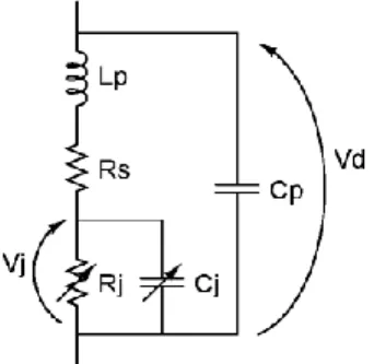
The Shockley diode model with added packaging parasitic components presented in Figure 2-2 is considered during the development done in this work [17]. In this model, Rs is the series linear resistance, Rj is the nonlinear junction resistance whose current can be calculated by using (2.1) [18], Cj is the nonlinear junction capacitance and Cp and Lp are the packaging parasitic capacitance and inductance, respectively. The packaging parasitic components are only considered in the matching calculations. Although Cj may be bias-dependent, it is considered to be constant for the low-power evaluation described in this paper.
Figure 2-2: Diode model considered in the developments described in this article
1 j T V V j j s I V I e (2.1) where T N k T V q is the thermal voltage, with the diode’s ideality factor N already embedded for simplification purposes, q is the electron charge, k is the Boltzmann constant, T is the temperature of operation, Is is the diode’s reverse saturation current, and Vj is the voltage applied to the diode’s junction.
2.2.3 DC source-to-load power transfer efficiency
To evaluate the dc behavior, the diode junction can be modeled through the use of the Thévenin or Norton equivalent circuits as shown in Figure 2-3.
In the Norton equivalent circuit, the total rectified current Ijdc is divided between the dc load
RL which is in series with the diode’s series resistance Rs, and the parallel diode’s junction
resistance Rj. The dc current at the load, Iload, can be calculated by the following equation:
0
.
0 j load load jf jdc jf S j load L R I I V I V R R I R (2.2)where Vjf0 is the excitation voltage over the diode’s junction at the fundamental frequency f0 and
Ijdc is the total dc current rectified by the diode junction.
Diode Diode VjDC Rs Rj RL Iload Rs Rj RL Iload IjDC (a) (b)
Figure 2-3: (a) Thévenin and (b) Norton equivalent circuits for the diode junction working as a dc power supply.
The total dc power generated by the diode, Pdc, is calculated using Iload (2.2) and the resistive loads at the dc current path. This can be calculated through the diode model given in Figure 2-2 and the series load RL, as given by circuit in Figure 2-3 (a).
2 0.
dc L s j load load jf
P R R R I I V (2.3)
And the dc power delivered to the load, Pload, by:
2 0 . L load load jf P R I V (2.4)So the DC source-to-load power transfer efficiency can be calculated by:
( ) d load L SL L s j load c P R P R R R I (2.5)
2.2.4 RF-to-dc power conversion efficiency
Most of the published RF and microwave power harvester models, which describe the RF-to-dc power conversion efficiency, consider the diode as a perfect switch whose impedance approaches RS, the diode’s series resistance when directly polarized, and infinity when reversely polarized [17, 19]. This method delivers good results when the input signal is relatively large, usually in the mW range and above, and the investigated diode has a high barrier leading to a large zero-bias resistance (ZBR) Rj0. However, this method does not hold for very low input power levels, or for low barrier diodes which present a small ZBR in the order of tens of kΩ and below. As it may be seen in Figure 2-4 where the simulated junction resistance of the Skyworks SMS7630 [20] diode at -40 dBm is presented, the assumption that the diode works as a perfect switch is not true anymore. In such a typical low power driving condition, the diode’s impedance varies between 2 kΩ and 20 kΩ over time, not reaching neither a 0 Ω neither an infinitely large impedance state.
Figure 2-4: Simulation result of the junction resistance of a SMS7630 diode, input power is -40 dBm and load is 5 kΩ. Rj is calculated using δV/δI.
To model this non-linearity of Rj, the zero bias current responsivity
0
I
will be used in this work. The current responsivity (2.6) is defined as the ratio between the output dc current Ijdc and the input RF power Pf0 [18] for a 0Ω load. The usual derivations of0
I
however may only be used in the diode’s square law region. Thus, an extended version of the current responsivity that will be denoted by
*I and may be used out of the diode’s square-law region is proposed here.0 j I DC f I P (2.6) To find its extended form, the diode’s I-V characteristic, given by (2.1) is extended in a Taylor series. In a Taylor expansion around the 0 V point:
1 1 2 1 . 1! 2! ! n j j j s T j j T T V V V V I V I V n V (2.7) Assuming that the applied signal is a constant sinusoidal wave with fundamental frequency f0, one can write Vj as
0 sin 2 . 0. j jf
V V
f t (2.8)Substituting (2.8) into (2.7), and isolating only the terms in dc and in the fundamental frequency, one can find the dc current generated at the junction, Ijdc, and the current at the fundamental frequency, Ijf0. The power that reaches the diode junction at the fundamental frequency, Pjf0, can then be found using equation (2.9).
0 1 0 0 0 0 0 2 4 6 2 0 0 0 0 . 1 1 1 1 2 8 192 9216 f jf f j jf jf jf jf jf T T T T P V f V I dt V V V V V V V V
(2.9)Using Ijdc and casting (2.9) into (2.6), one can obtain the extended current responsivity, which can be written as
0 0 0 2 4 0 0 * 0 2 4 0 0 1 1 1 16 576 1 2 1 1 1 8 192 1 . 2 I I jf jf T T I jf T jf jf T T I T V V V V V V V V V V V (2.10) where 0 I
is the diode’s zero-bias current responsivity. This extended responsivity equation results from the current-voltage relationship given in (2.1). What’s remarkable about (2.10) is that the only diode intrinsic characteristic having an impact on the current responsivity is the diode’sideality factor N, embedded into VT.
0
I
. This is inversely proportional to N and has a maximum equal to 19.34 A/W at 300K. This is the maximum current responsivity that any Schottky diode can reach at the ambient temperature, thereby standing for an important limitation in the use of Schottky diodes for low power energy harvesters. A recently published microwave power rectifier using heterojunction backward tunnel diodes with current responsivities in the order of 22 A/W has demonstrated how such a technology can be used to break through this Schottky diode limitation, thus greatly improving the microwave power harvester efficiency [10].Equation (2.10) also depends upon the external parameter Vjf0. As the denominators from the lower polynomial are smaller than the counterpart from the upper polynomial,
*I decreases whenVjf0 increases, thus, when the input power increases. This decrease in responsivity can be understood by looking at Figure 2-5 where the simulated SMS7630 current responsivity is given together with two different amplitude Vj signals. The smaller amplitude signal remains in a maximum
I region. When the applied signal amplitude increases, the diode starts to operate in regions with a reduced
I. If one thinks of the total
*I as an average responsivity for the voltages through which the junction is excited, the average would then decrease with the increasing excitation amplitude. This variation of
*I as a function of the external excitation is represented byin equation (2.10).
In order to calculate the total dc current generated at the diode junction Ijdc, equations (2.10) and (2.6) are used for a given junction voltage Vjf0. The junction power Pjf0 is then found by using (2.9) for this same value of Vjf0. This method can be used for low input power levels, ranging up to few µW of input power. The model becomes less accurate for an increasing power because of the simplification assumed in (2.8) where the harmonics and dc bias in the diode junction voltage were ignored. This range, however, is enough for ambient microwave energy harvesting aplications and can be extended as it will be further presented in section 2.2.8.
The presented equations can be used to calculate the total dc current generated by the diode junction, Ijdc given the power arriving at the diode’s non-linear junction. In order to calculate the
total dc power delivered to the load, the effects of the dc source-to-load power transfer have to be considered as shown in section 2.2.3.
Figure 2-5: Top part: Two sine waves, representing the voltage applied to the diode terminals. Bottom part: Simulated current responsivity of the SMS7630 diode for a voltage sweep near the
zero-bias condition.
The total dc power generated by the diode, Pdc, can then be calculated using Iload (2.2) and the equivalent resistance at the dc current path. This can be calculated using the Thévenin equivalent circuit in which the diode is in series with the load, as described by (2.3). Defining the RF-to-dc power conversion efficiency as the total dc generated power divided by the power that reaches the junction, one can write the following,
0 0
2 2 0 0 ( ) . . . ( ) I j load DC RFdc I jf jf L s j load R I P P P R R R I (2.11)Equations (2.5) and (2.11) may be used to determine the optimum load value with which the maximum efficiency in the RF-to-dc power conversion efficiency is reached. In Annex A, it is shown that the load value for which the maximum efficiency is obtained is equal to Rs+Rj(Iload). This can be simplified to Rj(Iload) within the square-law operation limits as Rs is much smaller than
2.2.5 Parasitic Efficiency
Due to the low-pass filter effect of the diode’s junction capacitance Cj0, some of the RF current that reaches the diode is shunted, therefore dissipating power in the series resistance Rs. The total RF power that is delivered to the diode may be calculated by adding the power that reaches its junction (2.9) to the power that is dissipated by the diode’s series resistance Rs. The later may be calculated using equation (2.12), which can be derived by using simple linear circuit theory.
2 0 0 0 0 0 1 . 2. .2. . . . 2 s jf R s j jf jf P P R j f C V V (2.12)
The parasitic efficiency can be defined as the ratio between the total power supplied to the diode and the power that reaches the nonlinear junction, which may be expressed by
0 0 s jf parasitics jf R P P P (2.13)
Equations (2.12) and (2.13) can be simplified for the square-law region, where the junction resistance is considered to be constant and equal to Rj0, the resulting equation is given in (2.14) and was already given in [9, 18].
2 2 0 0 0 1 1 2 parasi j j ti s s c f C R R (2.14)Equations (2.5), (2.11) and (2.13), which are used to calculate ηSL,ηRFdc and ηparasitics respectively, describe the power conversion efficiencies related to the diode parasitic components and non-linearity. Assuming that the optimum load is chosen such that RFDCSL is maximized, one can assume from equation (2.11) that diodes with higher Rj will reach higher efficiencies. In equation (2.14), however, the impact of a higher Rj0 is seen to decrease efficiency. Finally, as it will be shown subsequently, the zero bias resistance value also plays a key role in the matching network losses. Those three tendencies will be analysed in the next session and the matching network insertion losses impact on the total rectifier PCE is evaluated in detail.
2.2.6 Matching Efficiency
The matching network insertion loss, or in turn, matching efficiency ηm, plays a significant role when determining the optimum diode for an ambient microwave power harvester. While (2.11)
indicates that a diode with a high Rj0 is expected to deliver a higher RF-to-dc power conversion efficiency, it is shown that ηm is inversely proportional to Rj0. Using the given model, an optimum
Rj0 where ηm•ηRFdc•ηSL is maximized can be suggested, indicating the optimum diode’s zero-bias junction resistance.
A prior knowledge of the matching network technology in terms of transmission line attenuation and propagation constants as well as lumped components quality factors, can be used to estimate the matching efficiency ηm as follows [21],
1 1 m r m Q Q (2.15) 1 HIGH r LOW R Q R (2.16)
where RHIGH and RLOW are the highest and lowest real impedances chosen from the source or the load, being typically the source impedance and Rj, respectively, when matching a diode. Qr is
called the required quality factor while Qm is the matching network quality factor that is actually obtained.
Finding the value of Qm can be simplified by approximating the diode by a parallel Rd//Cd circuit at the operation point of interest, which is determined by the input power and f0. In this case,
Rd is the equivalent parallel diode resistance to which the power is delivered and the equivalent parallel capacitance Cd will be absorbed into the matching network losses and bandwidth calculations. For a center frequency of interest, Rd and Cd may be calculated using the equations below, while maintaining the equivalent load quality factor [21]:
2
Re[
] (1
)
d diode diodeR
Z
Q
(2.17) 2 0 Im[ ] (1 ) 2 diode d diode Z C Q f (2.18)where Zdiode is the input impedance of the diode alone at f0 and the input power level of interest, and Qdiode is the quality factor of the diode, calculated at the same frequency and power. For frequencies far below the diode cut-off frequency, it can be approximated by:
Im[ ] Re[ ] diode diode diode Z Q Z (2.19)
To obtain the quality factor of the matching network, its input impedance as a function of frequency Zmatch(f) needs to be calculated, with the first component of the matching network being Cd. Once this equation is known, Qm may be calculated using one of the two equations below [22]:
Im[ ( )] Im[ ( )] 1 ( ) 2 Re[ ( )] match match m match d Y f Y f f df Q f Y f (2.20) Im[ ( )] Im[ ( )] 1 ( ) 2 Re[ ( )] match match m match d Z f Z f f df Q f Z f (2.21)
where Ymatch(f) is the input admittance of the matching network, given by 1/Zmatch(f). Equation (2.20) is used when the matching network behaves as a parallel resonator near f0, while equation (2.21) is used when the behaviour resembles a series resonator.
Every component used in the matching network’s Zmatch(f) calculation needs to have its
contributing parasitic parts included. When transmission line distributed components are used, the complex characteristic impedance of the line Zc needs to be used. In [23], for example, it is shown that the quality factor of a short stub can vary by a factor of 2 if a simplified real impedance is used instead of the complex impedance of the transmission line.
When transmission lines are used as components of the matching network, it is important to take into account the effect that the standing waves have on losses. The increased voltage and current that appear on the line would introduce higher losses to the system. In [24], it is shown that an equivalent transmission line attenuation constant αr can be calculated, which will account for these increased losses. αr is related to the matched transmission line attenuation constant αm by the following equation: 2 1 2 r m r r
(2.22)where r is the standing wave ratio sustained by the transmission line, which is usually calculated using (2.23), where ΓL is the reflection coefficient at the load side.
1 1 L L r (2.23)
However, since transmission lines used in the design of matching networks are usually shorter than half-wavelength, it is not possible to assume that both maximum and minimum current and
voltage nodes will appear in the standing wave sustained in the transmission line under consideration. For this reason, equation (2.23) cannot be used.
Zs Zc ZL
Γ1 Γ2 Γ3
Vin
l z
0
Figure 2-6: Travelling wave approach used to calculate the standing wave ratio in a transmission line of length l.
Using the travelling wave formulation, one can calculate the voltage at a short length of transmission line with reflection at both ends. Assuming a transmission line with propagation constant γ, characteristic impedance Zc and length l, connected to a source with impedance ZS and a load with impedance ZL, as shown in Figure 2-6, one can write the voltage on the transmission line Vl as a function of the position z as given by equation (2.24).
2 2 3 2 3 2 4 2 2 4 2 3 2 3 ... ( ) ... z l z l z l in l z l z e e e e e V z V e e e e (2.24)
which can then be simplified to (2.26) by using (2.25).
0 1 1 n n x x
for |x| < 1 (2.25)
2
3 2 2 3 ( ) 1 z z l l in l e e e V z V e (2.26)Using the points where the first derivative of (2.26) with respect to z equals 0, one can find the positions where |Vl(z)| has a maximum or a minimum point. In Annex B, it is shown that this
happens for: atan( / ) 2 n D C z
(2.27) where 2 3 ( ) l e C Di , β is the transmission line’s phase constant and n is an integer equal or greater than 0.