Comprehension and optimisation of the co-evaporation deposition of Cu(In,Ga)Se2 absorber layers for very high efficiency thin film solar cells
Texte intégral
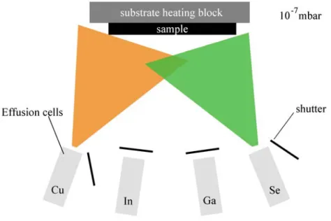
Figure

![Figure 1.1.: CIGS solar cell and module efficiency development. Data is taken from the Solar cell efficiency tables [9] published two times a year by Green et al](https://thumb-eu.123doks.com/thumbv2/123doknet/7764568.255716/16.892.178.688.580.862/figure-module-efficiency-development-solar-efficiency-tables-published.webp)
![Figure 1.4.: Solar cell parameters as a function of the Ga content for CIGS solar cells fabricated by co-evaporation [44].](https://thumb-eu.123doks.com/thumbv2/123doknet/7764568.255716/21.892.257.668.673.922/figure-solar-parameters-function-content-cigs-fabricated-evaporation.webp)


![Figure 2.1.: Absorption coefficients for CIGS absorber layers with varied GGI ratio [84].](https://thumb-eu.123doks.com/thumbv2/123doknet/7764568.255716/31.892.214.714.409.820/figure-absorption-coefficients-cigs-absorber-layers-varied-ratio.webp)
![Figure 2.3.: Band diagram of a p -type absorber/ n -type buffer/ n -type window structure between two metallic contacts after [20].](https://thumb-eu.123doks.com/thumbv2/123doknet/7764568.255716/34.892.131.731.585.870/figure-diagram-absorber-buffer-window-structure-metallic-contacts.webp)


Documents relatifs
Complementary, ex- situ analysis of structural properties via X-ray or neutron diffraction techniques gives the means to confirm (micro)structural film properties and to obtain
The activation energy of the temperature ‐dependent dark current density at fixed forward bias was shown to correlate with the activa- tion energy of the main capacitance step
(a) Effective hole concentration and (b) effective mobility obtained by Hall analysis of polycrystalline Cu(In,Ga)Se 2 thin film absorbers grown on glass (black squares, solid..
In summary, whereas in Cu-poor devices, the diffusion of Cd or Zn chemical species results in the decrease of the absorber carrier con- centration after HT2, in Cu-rich CuInSe 2
All these issues pose new constrains on the development of alternative buffer layers or front passivation approaches beyond ensuring low absorptivity and excellent interface
This shift can be measured in angle-resolved photoluminescence (ARPL) experiments by tilting the sample by an angle u and collecting the photons that travel a different path through
The small yet meaningful change in qFls obtained when comparing KF-treated with Se-treated samples, made us question the impact of the high Ga content used in the Cu-series
For absorbers with a [Cu]/[In þ Ga] ratio below one, the measured quasi Fermi level splitting is 120 meV higher compared to absorbers grown under copper excess independent of
