HAL Id: hal-00665217
https://hal.archives-ouvertes.fr/hal-00665217
Submitted on 1 Feb 2012
HAL is a multi-disciplinary open access
archive for the deposit and dissemination of
sci-entific research documents, whether they are
pub-lished or not. The documents may come from
L’archive ouverte pluridisciplinaire HAL, est
destinée au dépôt et à la diffusion de documents
scientifiques de niveau recherche, publiés ou non,
émanant des établissements d’enseignement et de
3D Multiprocessor with 3D NoC Architecture Based on
Tezzaron Technology
Mohammad Jabbar, Dominique Houzet, Omar Hammami
To cite this version:
Mohammad Jabbar, Dominique Houzet, Omar Hammami. 3D Multiprocessor with 3D NoC
Architec-ture Based on Tezzaron Technology. IEEE International 3D System Integration Conference (3DIC),
Jan 2012, Osaka, Japan. 3D Applications - p.2-18. �hal-00665217�
3D Multiprocessor with 3D NoC Architecture Based
on Tezzaron Technology
M.H Jabbar
1,2, D. Houzet
1, O. Hammami
2 1GIPSA-Lab, 11 Rue Des Mathematiques,
BP 46, F-38402, Saint Martin D’Heres, FRANCE
2
ENSTA ParisTech, 32 Bvd Victor, 75739, Paris, FRANCE
Abstract-In this paper, we describe the architecture and
implementation of 3D multiprocessor with 3D NoC. The 2 tiers design is based on 16 processors communicating using a 4x2 mesh NoC and will be fabricated using Tezzaron technology with 130 nm Global Foundaries low power standard library. Due to the limitation when investigating NoC performance using simulation, the purpose of this work is to accurately measure NoC performances in real 3D chip when running mobile multimedia applications to evaluate the impact of 3D architecture compared to 2D.
Keywords – 3D IC, 3D NoC, MPSoC, Tezzaron
I. INTRODUCTION
As moving to sub-20 nm CMOS poses great design and manufacturing challenges, 3D integration is seen as an alternative to increase transistor density for complex application to meet high performance demand without facing many problems as seen by scaling CMOS. By stacking dies or wafers, we can increase the performance because overall wirelength is reduced and so is power consumption. Stacking multiple dies will also reduce the total footprint of a chip making it very suitable for mobile devices. However, several challenges such as thermal and testing of 3D architectures need to be overcome before 3D technology can be implemented in consumer devices [1].
II. RELATED WORK
Many issues in 2D NoC architecture and design have been studied for the past several years such as design flow, implementation evaluation and design space exploration [2] [3] [4] [5]. However, 3D NoC architectural evaluation is limited as the technology is still under active research many organizations. In [6], they reported 3D NoC performance evaluation for data parallel of H.264 design experimenting using cycle accurate simulator, showing improvement of about 34% over 2D architecture. Apart from that, design of asynchronous 3D NoC router also has been proposed to reduce TSV numbers using serializing method while providing higher speed inter-die packet transfers [7].
Despite performance evaluation of 3D architecture have been conducted using simulation [8] [9] [10], there is still a need for real 3D architecture implementation to accurately
measure the performance as well as to validate the simulation results. Several 3D architectures have been designed and fabricated previously. T. Zhang et al developed a SoC architecture in 3D for H.264 application using Tezzaron technology [11]. Healy et al fabricated a multiprocessor architecture consisting of 64 cores with instruction memory in one layer and a total of 256 KB SRAM memory in another one layer. Buffer based architecture is used for inter processor communication [12]. Van Der Plas et al, Loi et al and Mineo et all have also demonstrated 3D architecture focusing on NoC architecture [13] [14] [15]. Their work focused on demonstrating the TSV for inter die signalling and TSV characterization which is not the aim in this work.
Our objective is to design a 3D multiprocessor chip with 3D NoC architecture on 2 tiers and to measure the performances when running applications primarily for evaluating NoC communication in real 3D architecture. This is also done to validate the simulation of parallel applications in 3D NoC architecture. The design will be sent for fabricated using Tezzaron 2 tiers face to face stacking technology through CMP [16].
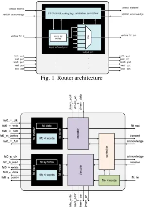
III. ROUTER ARCHITECTURE
The input buffered-based router architecture is shown in Fig. 1. It has 4 neighbouring ports, one vertical port for connecting to another tier and one local port to the processor through network interface unit which has a total area of 0.185 mm2 from synthesis estimation. Each input/output port has 35 bits data flits and 2 bits control signals for packet transfer between routers. Normal handshake protocol is used for router to router communication and router to network interface communication. The network interface architecture shown in Fig. 2, connects processor to router through a FIFO port and has an area of 0.062 mm2. Based on data address and number of words to be included in the packet, the network interface will access the processors data memory to process data blocks through DMA. Each network interface unit connects to processor through 2 FSL ports (FIFO); one master FSL for writing data to be transferred and the other one slave FSL for reading synchronization flags from other processors. The synchronization FIFO has 16 words (one words per processors) and 5 bits wide. There
is one 11 bits counter in the network interface unit for measuring packets travel timing. The timing information is included in the header flit attached when the packets enter the network as shown in Fig. 3 and is processed when the packets arrive at the destination network interface. Both the network interface and router can be run at 300 MHz maximum frequency.
Each input port has one buffer built using 16 words FIFO based dual port RAM architecture to support a maximum of 16 data blocks transfer. As XY routing is deadlock free and we do not implement priority packets transfer, the virtual channel implementation is not useful. We use round robin arbitration for output port selection when there is more than one input requesting the same output route. Wormhole switching method is used for packet transfer in the NoC because it does not require large buffer and has lower latency. For the routing, deterministic coordinate based routing is implemented using XYZ coordinate where each packet will travel first in the X direction followed by Y direction and finally through Z direction (vertical). We use multiplexer based crossbar because it uses less area as well as less power compared with matrix crossbar. Each router has vertical port for connection to other router in the top tier using microbumps.
Fig. 1. Router architecture
e n c o d e r d e c o d e r c o n tr o lle r fs l m a s te r fs l s la v e d a ta _ w ri te d m e m _ a d d r d m e m _ d a ta d m e m _ a d d r d m e m _ e n d m e m _ e n d m e m _ w e fs l m a s te r fs l s la v e
Fig. 2. Network interface architecture
. .
.
Fig. 3. Packet format for the NoC
Register File 32 words ALU MUL Program Counter FSL Master FSL Slave Instruction decode Fetch IMEM address IMEM data
Fig. 4. Openfire processor architecture IV. PROCESSOR ARCHITECTURE
We use an open source processor for our implementation which is readily available without spending much time to develop a new processor. The Openfire processor as shown in Fig. 4, is downloaded from Opencores.org [17]. It is a Microblaze clone which supports Microblaze ISA and compiler tool chain. It supports hardware multiplier only. Although there are other open source synthesizable Microblaze clones available, we choose Openfire because it has FSL ports (FIFO ports) that we need for simple data and synchronization communication between processors and NoC rather than using more complex interface such OCP and AXI which require complex logic. The Openfire processor is a simple processor developed initially for configurable processor research [18]. Thus, because of its simplicity, it will not require a large area and thus can be used to develop any small application for testing the NoC in 3D architecture. We use only 4 KB for instruction and 4KB for data memory in order to limit the die area. These memories are generated using Artisan memory compiler. The processor can be run at 100 MHz at maximum frequency and has an area of 0.158 mm2.
V. 3D 2 TIER 16PE MULTICORE
Our architecture as shown in Fig. 6 consists of two face to face tiers. Each tier has 8 processors connected using 4x2 NoC using a mesh network. Connection in each tile block in shown in Fig. 7. Connection between tiers is achieved using vertical ports of each router. Total tier to tier connection is 594 connections (35 bits flit data + 2 tx/rx signals + 2 JTAG signals for one direction vertical port router) for all 8 routers
in one tier in two directions. Connections are made with 594 microbumps connecting the two face to face tiers from the total of about half million available vertical connection. The microbumps are created from metal 6 layer of both tiers.
Synchronization between processors is implemented using FSL linked to the NoC. Processors communicate together through their data memory. A processor will synchronize before accessing its data memory by waiting for a tag word in its FSL sent by the writer processor. This is a simple synchronization hardware implementation in order to reduce die area.
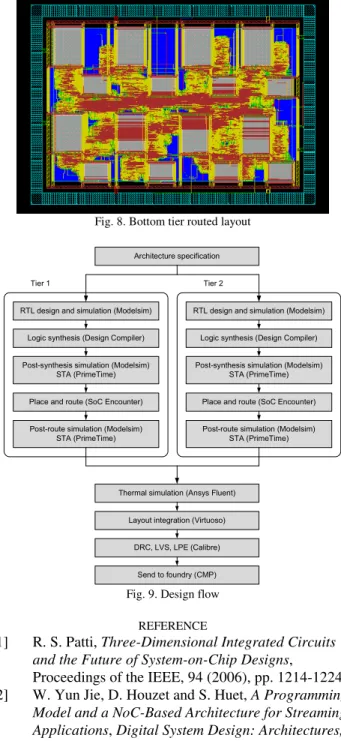
In overall, our design fit into 5.2 mm x 5.2 mm die area for each tier. Network interface units use 15.39% of total area while 3D router and processors use 45.5% and 38.86% respectively. Target frequency for functional operation is 166 MHz (6 ns clock) and 10 MHz for test operation. The layout of bottom tier is shown in Fig. 8, which is not much different from the top tier (without JTAG controller block).
We use an IEEE 1149.1 JTAG port for off chip interface. The JTAG controller is located at the bottom die and connected to outside chip using TSV under the I/O pad. Loading instruction and data memory for each processor is also using the JTAG port. Also the data memory of one processor (id 0) is connected outside in order to have fast access to results and be able to provide new input data.
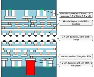
The TSV technology from Tezzaron called FaStack is used here only for I/O pads made from Tungsten. It has 1.2 um diameter, 5 um pitch and 6 um depth. The two tier 3D stacking method is based on wafer to wafer bonding with via first approach shown in Fig. 5. TSV liner is using Silicon Oxide to insulate from Silicon substrate. The wafer is bonded before thinning and thus there is no wafer handling required.
The design flow for 3D architecture design is based on 2D EDA tools as shown in Fig. 9. The important step is specification where we decide the components for each tier. In this design partitioning method is easy as we have the same architecture for both tiers except for the JTAG controller block. Each tier can be synthesized and placed and routed separately and thus can be done in parallel. During floorplanning stage, we need to capture the location of microbumps for inter tier connection such that we could connect the same signal to the same bump on the other tier with mirroring. This microbumps location also has to honour for power ground wires. Once the designs have been routed, we can integrate them in the Virtuoso environment for signoff 3D DRC and 3D LVS before submit to the foundry. Timing analysis for post synthesis and post-layout is done using Synopsys PrimeTime. As the inter-die delay is very small (microbumps delay), we can have early estimation of the 3D architecture performance after the synthesis of both tiers.
VI. CONCLUSION
We have described the architecture of two tiers 3D multiprocessor with NoC architecture consists of 16
processors using 4x2x2 mesh NoC architecture which will be sent for fabrication through CMP. The NoC architecture supports block data transfers for large data communication between processors. Initial experiment to evaluate performance of parallel applications in 3D NoC is being carried out and real measurements or the applications can be obtained after the chip is fabricated.
VII. ACKNOWLEDGMENT
Mohamad Hairol Jabbar is supported by Ministry of Eduction (MOHE) Malaysia and Universiti Tun Hussein Onn Malaysia (UTHM).
Fig. 5. Tezzaron two tier technology
Fig. 6. 2 tier 3D mutiprocessor architecture
Fig. 8. Bottom tier routed layout Architecture specification
RTL design and simulation (Modelsim)
Logic synthesis (Design Compiler)
Post-synthesis simulation (Modelsim) STA (PrimeTime)
Place and route (SoC Encounter)
DRC, LVS, LPE (Calibre) Post-route simulation (Modelsim)
STA (PrimeTime)
Layout integration (Virtuoso)
Send to foundry (CMP) Tier 1
RTL design and simulation (Modelsim)
Logic synthesis (Design Compiler)
Post-synthesis simulation (Modelsim) STA (PrimeTime)
Place and route (SoC Encounter)
Post-route simulation (Modelsim) STA (PrimeTime) Tier 2
Thermal simulation (Ansys Fluent)
Fig. 9. Design flow REFERENCE
[1] R. S. Patti, Three-Dimensional Integrated Circuits
and the Future of System-on-Chip Designs,
Proceedings of the IEEE, 94 (2006), pp. 1214-1224. [2] W. Yun Jie, D. Houzet and S. Huet, A Programming
Model and a NoC-Based Architecture for Streaming Applications, Digital System Design: Architectures,
Methods and Tools (DSD), 2010 13th Euromicro Conference on, 2010, pp. 393-397.
[3] S. Evain, J. P. Diguet and D. Houzet, uspider: a CAD
tool for efficient NoC design, Norchip Conference,
2004. Proceedings, 2004, pp. 218-221.
[4] L. Zhang, V. Fresse, M. Khalid, D. Houzet and A.-C. Legrand, Evaluation and Design Space Exploration
of a Time-Division Multiplexed NoC on FPGA for
Image Analysis Applications, EURASIP Journal on
Embedded Systems, 2009 (2009).
[5] M. H. Jabbar and O. Hammami, Performance
Analysis of a NoC-based 16PE Embedded Multicore:
Processor Configuration Impact, International
Design and Test, IDT 2010, IEEE, Abu Dhabi, 2010.
[6] T. C. Xu, A. W. Yin, P. Liljeberg and H. Tenhunen,
A study of 3D Network-on-Chip design for data
parallel H.264 coding, NORCHIP, 2009, 2009, pp.
1-6.
[7] F. Darve, A. Sheibanyrad, P. Vivet and F. Petrot,
Physical Implementation of an Asynchronous 3D-NoC Router Using Serial Vertical Links, VLSI
(ISVLSI), 2011 IEEE Computer Society Annual Symposium on, 2011, pp. 25-30.
[8] V. F. Pavlidis and E. G. Friedman, 3-D Topologies
for Networks-on-Chip, Very Large Scale Integration (VLSI) Systems, IEEE Transactions on, 15 (2007), pp. 1081-1090.
[9] K. Nomura, K. Abe, S. Fujita, Y. Kurosawa and A. Kageshima, Performance analysis of 3D-IC for
multi-core processors in sub-65nm CMOS technologies, Circuits and Systems (ISCAS),
Proceedings of 2010 IEEE International Symposium on, 2010, pp. 2876-2879.
[10] B. S. Feero and P. P. Pande, Networks-on-Chip in a
Three-Dimensional Environment: A Performance
Evaluation, Computers, IEEE Transactions on, 58
(2009), pp. 32-45.
[11] Z. Tao, W. Kui, F. Yi, C. Yan, L. Qun, S. Bing, X. Jing, S. Xiaodi, D. Lian, X. Yuan, C. Xu and L. Youn-Long, A 3D SoC design for H.264 application
with on-chip DRAM stacking, 3D Systems
Integration Conference (3DIC), 2010 IEEE International, 2010, pp. 1-6.
[12] M. B. Healy, K. Athikulwongse, R. Goel, M. M. Hossain, D. H. Kim, L. Young-Joon, D. L. Lewis, L. Tzu-Wei, L. Chang, J. Moongon, B. Ouellette, M. Pathak, H. Sane, S. Guanhao, W. Dong Hyuk, Z. Xin, G. H. Loh, H. S. Lee and L. Sung Kyu, Design and
analysis of 3D-MAPS: A many-core 3D processor with stacked memory, Custom Integrated Circuits
Conference (CICC), 2010 IEEE, 2010, pp. 1-4.
[13] G. Van der Plas, P. Limaye, I. Loi, A. Mercha, H. Oprins, C. Torregiani, S. Thijs, D. Linten, M. Stucchi, G. Katti, D. Velenis, V. Cherman, B. Vandevelde, V. Simons, I. De Wolf, R. Labie, D. Perry, S. Bronckers, N. Minas, M. Cupac, W. Ruythooren, J. Van Olmen, A. Phommahaxay, M. de Potter de ten Broeck, A. Opdebeeck, M. Rakowski, B. De Wachter, M. Dehan, M. Nelis, R. Agarwal, A. Pullini, F. Angiolini, L. Benini, W. Dehaene, Y. Travaly, E. Beyne and P. Marchal, Design Issues and
Considerations for Low-Cost 3-D TSV IC
Technology, Solid-State Circuits, IEEE Journal of, 46 (2011), pp. 293-307.
[14] I. Loi, P. Marchal, A. Pullini and L. Benini, 3D NoCs
- Unifying inter and intra chip communication,
IEEE International Symposium on, 2010, pp. 3337-3340.
[15] C. Mineo, R. Jenkal, S. Melamed and W. R. Davis,
Inter-die signaling in three dimensional integrated circuits, Custom Integrated Circuits Conference,
2008. CICC 2008. IEEE, 2008, pp. 655-658.
[16] Tezzaron Design Kit, CMP, http://cmp.imag.fr. [17] Openfire Processor Core,
(http://opencores.org/project,openfire_core).
[18] S. Craven, C. Patterson and P. Athanas, Configurable
Soft Processor Arrays Using the OpenFire Processor, Proceedings of the 8th Annual
Conference on Military and Aerospace
Programmable Logic Devices, MAPLD 2005,