HAL Id: hal-02366907
https://hal.archives-ouvertes.fr/hal-02366907
Submitted on 16 Nov 2019
HAL is a multi-disciplinary open access
archive for the deposit and dissemination of
sci-entific research documents, whether they are
pub-lished or not. The documents may come from
teaching and research institutions in France or
abroad, or from public or private research centers.
L’archive ouverte pluridisciplinaire HAL, est
destinée au dépôt et à la diffusion de documents
scientifiques de niveau recherche, publiés ou non,
émanant des établissements d’enseignement et de
recherche français ou étrangers, des laboratoires
publics ou privés.
Ultrathin Eu- and Er-Doped Y2O3 Films with
Optimized Optical Properties for Quantum Technologies
Marion Scarafagio, Alexandre Tallaire, Klaas-Jan Tielrooij, Daniel Cano,
Andrey Grishin, Marie-Hélène Chavanne, Frank Koppens, Armelle Ringuede,
Michel Cassir, Diana Serrano, et al.
To cite this version:
Marion Scarafagio, Alexandre Tallaire, Klaas-Jan Tielrooij, Daniel Cano, Andrey Grishin, et al..
Ultrathin Eu- and Er-Doped Y2O3 Films with Optimized Optical Properties for Quantum
Technolo-gies. Journal of Physical Chemistry C, American Chemical Society, 2019, 123 (21), pp.13354-13364.
�10.1021/acs.jpcc.9b02597�. �hal-02366907�
1
Marion Scarafagio
*a,e, Alexandre Tallaire
a, Klaas-Jan Tielrooij
b,c, Daniel Cano
b, Andrey Grishin
a,
Marie-Hélène Chavanne
a, Frank H. L. Koppens
b,d, Armelle Ringuedé
a, Michel Cassir
a, Diana
Ser-rano
a, Philippe Goldner
aand Alban Ferrier
*a,ea
Institut de Recherche de Chimie Paris (IRCP), Université PSL, Chimie ParisTech, CNRS, 75005 Paris, France
b
ICFO – Institut de Ciències Fotòniques, The Barcelona Institute of Science and Technology, Castelldefels, Barcelona, Spain
c
Current affiliation: Catalan Institute of Nanoscience and Nanotechnology (ICN2), Barcelona Institute of Science and Technolo-gy, Campus UAB, Bellaterra, 08193 Barcelona, Spain
d
ICREA Institucio Catalana de Recerca I Estudis Avancats, 08010 Barcelona, Spain
e
Sorbonne Universités, Faculté des Sciences et Ingénierie, UFR 933, 75005 Paris, France
ABSTRACT: Atomic Layer Deposited (ALD) Y2O3 thin films have been thoroughly investigated for optical or electronic
applications. The coherent spectroscopy of lanthanide ions doped into this material has also recently attracted an increas-ing interest in the field of quantum technologies for which they are considered promisincreas-ing candidates in quantum memo-ries or as spin-photon interface. However, these most demanding applications require a deep control over the local posi-tioning of the ions and their close environment in the crystalline matrix. This study focuses on the structural as well as optical properties of Eu3+ and Er3+ dopants in Y2O3using photoluminescence (PL), luminescence decay times and
inhomo-geneous linewidth (Γinh) measurements within this particular context. While as-grown ALD films do not provide an ideal
host for the emitters we demonstrate that by optimizing the deposition conditions and using appropriate annealing post treatments, narrow inhomogeneous lines can be obtained for the 7F0 ↔ 5D0 transition of Eu3+ even for nanoscale films.
Furthermore, about 1.5 ms lifetime has been measured for the infrared telecom transition of Er in ultrathin films (< 10 nm) which is an order of magnitude higher than in nanoparticles of the same size. These results validate optimized rare-earth doped ALD Y2O3 films as a suitable platform for photonics applications where few nm thick films with well localized
emit-ters are mandatory. This approach provides the first building blocks towards the development of more complex devices for quantum sensing or hybrid structures coupled to other systems such as 2D materials.
Rare earth (RE) oxides represent a technologically useful class of materials that can address a variety of applications such as photonics1,2,3, protective coatings4,5, laser media, catalysts6, scintillators and phosphors.1,7 They have also been highly studied for microelectronics in which high permittivi-ty dielectric films could advantageously replace SiO2 as gate
insulators.8,9 RE elements (Sc, Y and La-Lu) have similar chemical properties and close atomic radius allowing easily substituting one to another in a crystalline matrix and giving access to a wide range of compositions as well as high doping levels.
Recently, RE doped oxide crystals have attracted an in-creasing attention for quantum technologies (QT) that promise to overcome classical limits in a large range of appli-cations including communication, sensing, time stamping and computing.10 RE doped oxide crystals feature, at cryo-genic temperatures, a combination of exceptionally long optical and spin coherence times, e.g. 2.6 ms11 and 6 hours12 respectively together with a high PL stability without
blink-ing. Indeed, their optical emission consists of narrow and well-resolved lines that stem from the shielded 4f-4f transi-tions that are only weakly perturbed by the crystalline envi-ronment. Thanks to this, RE doped oxide crystals are the state-of-the-art materials for long storage time quantum memories13, entanglement storage14 and quantum state tele-portation between a telecom photon and a crystal.15
While bulk crystals are preferably used for QT, a strong in-terest has also emerged for RE ions inside nanostructures. 16,17 The availability of nanoscale particles18 or thin films, can open up many opportunities in this field. The coupling of these systems to resonators or hybrid structures as well as the fabrication of waveguides and photonic structures is greatly facilitated in this form.16,19 The ability to develop integrated quantum devices compatible with the silicon industry is also an important goal in the development of QT.20 In addition, the thin film approach allows optimizing precursor consumption and gives access to compositions and phases that can hardly be reached by bulk growth from the melt. However high crystallinity and purity films are required
2
whereas surface effects play an important role indecoher-ence.
RE:Y2O3 is currently the only nanosystem to exhibit long
optical and spin coherent lifetimes.18,21,22 Furthermore, thin films of Er:Y2O3 have for example been integrated into a new
demonstrate control of the energy transfer from erbium ions into graphene.23 The ability to grow few nanometer thick films combining high crystalline quality, optimal optical properties and precise spatial localisation is a key point to address to capitalize on these new hybrid devices.
Several techniques have been used to grow Y2O3 as thin
films9 on a variety of substrates including Pulsed Laser Depo-sition (PLD)24, Physical Vapour Deposition (PVD)25, Atomic Layer Deposition (ALD)8,26,27,28, Metalorganic Chemical
Va-pour Deposition (MOCVD)29 or Molecular Beam Epitaxy (MBE).30,31 Among those, ALD possesses many assets for depositing thin films with an accurate thickness control, the possibility to vary the doping level as well as a good uni-formity on standard silicon wafers or on any technologically relevant material platform. While the ALD synthesis of Y2O3
thin films is relatively well-known, the optical properties of RE elements (such as Eu or Er) doped into this matrix have yet not been thoroughly investigated within the context of QT.32,33 In particular no lifetime or inhomogeneous linewidth of sub 50 nm RE:Y2O3 ALD films have been reported to our
knowledge.
In study, we aim at demonstrating the potential of this ma-terial system as a platform for photonics in particular for very low thicknesses (< 20 nm). We determine the optimized deposition parameters but also the effect of post treatment on the film crystallinity. Furthermore, the structural analysis is correlated to optical properties in order to clarify how the deposition temperature affects the local environment of RE ions.
In this paper we report for the first time narrow inhomo-geneous linewidth of the 7F0 ↔ 5D0 of Eu in sub 100 nm films.
Furthermore we demonstrate that our strategy is versatile to other lanthanide ions since we observe a significant en-hancement of the lifetime of Erbium telecom transition even for 10 nm thick films.
Eu and Er doped Y2O3 thin films were grown in a Picosun
Sunale R200 using conventional β-diketonate precursors:
Y(tmhd)3 and Eu(tmhd)3 / Er(tmhd)3. They are thermally
stable and volatile and can be purchased with high purity (99.9 % STREM Chemicals). They however require a strong oxidizing agent that is provided by ozone (O3).26 To ensure
an efficient vaporization, the temperature of the tanks con-taining the precursors was maintained at 160 °C for Y(tmhd)3
and at 150 °C for the dopants throughout the deposition run. The doping level of the oxide films was finely tuned by se-quentially introducing pulses of the dopant elements in the standard yttrium oxide cycle. A typical ALD sequence con-sisted of a 3 s Y(tmhd)3 pulse followed by a 3 s purging pulse
of N2; a 3 s ozone pulse also followed by a 3 s N2 purge
(Fig-ure 1(a)). For a theoretical doping level of 5 %, when consid-ering an equivalent sticking coefficient for all precursors, 5 ALD cycles of Eu(tmhd)3 or Er(tmhd)3 were introduced for
every 95 ALD cycles of Y(tmhd)3. The final thickness was
precisely controlled in the range 10-375 nm by the number of cycles based on the calculated growth rate per cycle as
illus-trated in Figure 1(b). The self-limited regime was obtained for moderate temperatures of around 200-400 °C. Indeed, in this temperature range the film thickness increases linearly at about 0.21 Å per cycle. Furthermore, the linear behaviour and the zero offset visible in Figure 1(b) indicate a low nucle-ation activnucle-ation energy. The films were deposited on (100) Si wafers with an excellent thickness uniformity (better than 1 %) (Figure 1(c)). In order to improve the crystallinity of the films and the optical properties of the emitters, we investi-gated the process conditions and the use of a post-growth annealing treatment under O2 atmosphere (600 °C-1100 °C).
The crystallinity of the films was evaluated using X-ray Diffraction (XRD) in a Panalytical XPert Pro diffractometer with an incident beam Ge monochromator, and a stainless steel sample holder. Film thickness was measured by white light interferometry in the range 250-1000 nm with an Ocean
Optics NanoCalc system using Y2O3 optical constants.34 FEG
Scanning Electron Microscope (FEG-SEM) images of the surface of the films were recorded using a ZEISS Leo 15030 microscope. Photoluminescence (PL) measurements were performed in a Renishaw InVia micro-PL apparatus with a 50 × objective and a 532 nm laser as excitation source. Ca-thodoluminescence (CL) analysis was carried out at room temperature in a Horiba HClue system attached to a conven-tional SEM (Zeiss EVO MA15) using a 10 kV electron accelera-tion voltage and a 20 nA beam current. For the analysis we used a 600-groove grating with a 150 µm slit size for im-proved resolution. Decay measurements and time resolved PL were also recorded using a tunable optical parametric oscillator pumped by a Nd:YAG Q-switched laser (Ekspla
NT342B-SH) with 6 ns pulse length, a Jobin-Yvon HR250
monochromator and a photomultiplier tube. The detection time constant was 20 µs and data was recorded on a digital oscilloscope (Lecroy 332A).
Inhomogeneous linewidths of the 7F0 ↔ 5D0 transition were
measured in reflection mode in a helium bath cryostat (Janis
CTI-Cryogenics model CCS-150, LakeShore model 330
tem-perature controller) between 10 and 12 K. A low laser intensi-ty (1 mWcm-2) was used to avoid saturation of the transition and spectral hole burning. We performed fluorescence exci-tation (PLE) experiments by monitoring the red lumines-cence of the 5D0 → 7F2 transition (around 612 nm) for various
excitation wavelengths around 580.883 nm (516 098 GHz) provided by a Sirah Matisse DS laser, with a linewidth of 200 kHz. The red luminescence was filtered using at least 3 band pass filters and sent to a high sensitivity photomultiplier (PMT R5108 Thorlabs). In order to improve the signal to noise ratio the detection was performed with a lock-in ampli-fier. The lifetime of the 1.5 µm Er3+ transition in ultra-thin films was characterized in a confocal microscopy setup, where we excited with 532 nm laser light and measuredthe emission at 1.5 µm using a single photon counter (ID
Quan-tique 230 NIR). A square wave modulation to the 532 nm
excitation laser is applied and time-correlated single photon counting using a PicoHarp 300 is performed. Each laser trig-ger event and each detected 1.5 µm photon event have been recorded and used to construct a histogram during a time period of 10 minutes. The decay of the histogram after time zero (when the laser switches off) represents the lifetime of the erbium transition.
3
Figure 1 (a) Schematics of a typical ALD cycle used to grow RE-doped Y2O3 thin films, (b) Film thicknesses measured by white
light interferometry as a function of cycle number. The red line is a linear fit. (c) Image of a 2-inch Si wafer covered by a uniform Y2O3 ALD coating and showing a mirror-like surface.
RE sesquioxides are polymorphic materials with at least 5 different crystallographic structures.35 In the case of Y2O3,
monoclinic and cubic phases are usually observed. The cubic one (space group Ia-3) presents two cation sites with the local symmetry C2 and C3i whereas the monoclinic phase
(space group C2/m) have three crystallographically distinct cation sites, each having point group symmetry Cs.
35,36
For QTs, the cubic phase is preferred because the longest optical coherence lifetime (T2) of the
5
D0 → 7
F0 optical transition of
Eu has been measured for ions inserted in the C2 sites of the
cubic phase.
XRD analysis of the 5 % Eu doped Y2O3 films annealed at
different temperatures is presented in Figure 2 and compared with Y2O3 nanoparticles of the cubic phase obtained by
ho-mogeneous precipitation and annealed at 1200 °C.37 The agreement between the reference powder and the films dif-fraction peaks (Figure 2(a)) indicates that polycrystalline Y2O3 has been grown mostly in the cubic phase with
unde-tectable contribution from the monoclinic phase. The rela-tive intensity of the different peaks with respect to the ran-domly oriented nanopowders shows that diffraction from the (400) crystallographic planes is enhanced as compared to that from (222), (440) and (622) planes indicating a strong (100) texturing. This is consistent with previous reports on Y2O3 films grown by ALD on silicon.38 The effect of annealing
is particularly obvious when looking at the XRD pattern without normalization (Figure 2(b)). The intensity of the (400) diffraction peak is increased from 600 to 800 °C sug-gesting an improvement of the crystalline quality. However, above 950 °C, additional peaks (visualized by red arrows in Figure 2(a)) appeared and were attributed to the formation of a silicate phase (such as Y2SiO5 or Y2Si2O7) due to the
reaction of the oxide with the silicon wafer.39 This sets an upper limit for the annealing temperature to allow for an improvement of the crystalline quality without formation of parasitic phases. Deposition on other substrate materials or with a diffusion barrier could potentially provide a solution
to this limited annealing temperature but requires further study.
Additionally, on Figure 2(c), we observed that the diffraction peaks are shifted towards higher angles with respect to the reference which suggests a smaller lattice parameter than for a bulk material and thus compressive strain. Despite the lack of epitaxy, strain could be induced by the difference of lattice parameter between Si and Y2O3 which is about 2.4 %
be-tween a double Si lattice cell and a single oxide cell. The difference in thermal expansion coefficients (α) also induces strain upon heating and cooling since α is almost 3 times higher for Y2O3 than for Si. While annealing at a moderate
temperature of 600 °C increased the shift towards higher angles (lower graph of Figure 2(c)), it is noticeable that at higher temperatures, the trend became opposite with the diffraction angles still remaining higher than the reference (upper graph of Figure 2(c)). Both contributions (lattice parameter and thermal mismatch) should contribute to tensile strain which is not in agreement with the XRD result. It is thus believed that additional competitive mechanisms related to the presence of impurities in the films are at work that could reduce the effective cell parameter. A moderate temperature of 600 °C is enough to allow for the release of contaminants such as carbon, hydrogen or other impurities that can reach up to several % in ALD films grown with RE(tmhd)3 precursors,
38
thus possibly leading to a reduction of cell parameter. Further annealing at higher temperatures has a beneficial effect on the crystallinity of the films and this reorganization partially releases the accumulated stress. Further analysis of the chemical composition by XPS for example would be needed to confirm this explanation. A direct consequence of the induced stress is the apparition of cracks as illustrated in the SEM images of Figure 3. Alt-hough the as-deposited films always showed a smooth sur-face whatever their thickness, annealing at high tempera-tures (> 800 °C) led to the appearance of a network of cracks extending along specific crystalline directions particularly for thicker layers (> 100 nm). This indicates again the presence of thermally induced stress and is another limitation to the use of post-growth annealing treatments. However thinner of thermally induced stress and is another limitation to the use
4
of post-growth annealing treatments. However thinner oxidefilms annealed up to 950 °C do not exhibit cracks or parasitic phase formation which is encouraging for exploiting the optical properties of doped RE emitters as long as film thick-ness remains low enough.
Optical properties of RE oxides thin films or nanocrystals can differ from their bulk counterparts since due to a high surface to volume ratio, an important part of RE ions may be submitted to a varying crystalline environment. In this study, Eu3+ ions were used for structural investigation. Indeed, the narrow 7F0 →5D0 absorption line enables to probe the
disor-der and thus the crystalline quality of the host material.40,41 Moreover the main emission transitions 5D0 → 7F2, are forced
electric dipole transitions (ED) whereas the 5D0 → 7F1
pre-sents a magnetic dipole (MD) character.42,43 Slight modifica-tions of the symmetry are thus revealed by looking at the ratio between those 2 transition types since ED are much more sensitive to a distortion of the local surroundings than MD. For a low symmetry site like C2 in cubic Y2O3, the 5D0 → 7
F2 transition usually dominates the emission spectrum
(Fig-ure 4).
The films were analysed by standard luminescence char-acterization in PL using a 532 nm laser to excite Eu3+ ions to the 5D1 manifold. As expected, the resulting spectra are
dom-inated by emission from the 5D0 → 7F2 transition at 612 nm
(Figure 5(a)) corresponding to ions in the C2 site of the cubic structure of yttria.37 For as-grown films or films annealed at a low temperature, an additional contribution from the same transition but in a monoclinic lattice cell environment is visible at around 622 nm.42 When increasing the annealing temperature, this emission tends to disappear while the lines get narrower as judged by the linewidths (FWHM) reported in Figure 5(b). Although the emission remains broader by a factor of about 2 than that of a reference Eu3+:Y2O3 ceramic
with the same composition, a strong improvement of the film crystallinity with annealing is confirmed. Moreover, we observe a clear improvement of the luminescence intensity with the annealing temperature. Indeed an increase up to 10 has been observed between films of the same batch as grown and annealed at 950°C. At temperatures higher than 950 °C, PL spectrum of the Eu doped Y2O3 film shows new sets of
emission lines (Figure 5(c)). This is consistent with the para-sitic silicate phase due to reaction with the Si substrate,44 previously observed in XRD. The drastic change in crystalline
Figure 2 (a) XRD pattern normalized to the (400) diffraction peak, of Eu3+:Y2O3 films annealed at different temperatures. The
films thickness is 300 nm. Eu3+:Y2O3 cubic phase nanoparticles produced by homogeneous precipitation are used as a reference.
Silicate related peaks are highlighted by red arrows. (b) XRD pattern shown without normalization. (c) and (d) evolution of the (400) diffraction peak position with annealing temperature. * indicates XRD reflection from sample holder.
5
environment of the Eu emitters indeed leads to theappear-ance of strongly shifted emissions.
Figure 3 SEM images of the surface of 100 nm thick films (a)
and (b) and 375 nm thick films (c) and (d) before (left) and after (right) high temperature annealing of 900°C.
CL analysis of the films allows assessing emissions in a wider spectral range due to the broad excitation energies of the incoming electron beam. As illustrated in Figure 5(d) we confirmed the improvement of crystalline quality at moder-ate temperature and the clear change in emission spectrum at temperatures above 950 °C. Additionally, a broad charge transfer band which proceeds from transfer of an electron from the valence band to the 4f states of RE ions shows up in the UV range (250-350 nm) particularly at high annealing temperatures. This is consistent with a change in the crystal-line environment due to the formation of a new phase and the appearance of defect levels in the band gap. Besides, on the CL spectrum we observe an intense peak at 980 nm not attributed to Eu3+ ions transitions but possibly coming from Yb3+ impurities. Although this element has not been previ-ously introduced in the reactor chamber, the ALD precursors have 3N purity (99.9 %) only due to the difficulty in separat-ing different RE elements. It is thus probably the origin of this contamination. Inductively Coupled Plasma Mass Spec-trometry (ICP-MS) of Y(tmhd)3 precursor diluted in ethanol
(not shown here) confirmed that significant trace impurities of Yb3+ were present. This is a potential limitation for the use of our thin films in QT since the presence of RE impurities with an electron or nuclear spin could induce unwanted decoherence of close-by Eu3+ ions. Synthesis with higher purity precursors (4N or more) that are available but at a much higher cost could be needed.
From this first structural and spectral analysis, it is found that Eu:Y2O3 thin films with a controlled thickness and
dop-ing can be obtained on Si by ALD and that their crystalline and optical properties can be significantly improved by an-nealing at temperatures up to 950 °C. The formation of para-sitic phases due to reaction with the silicon substrate and stress leading to cracking for thicker films are limitations to the use of higher temperatures. In addition, the purity of commercial standard grade precursors is probably not suffi-cient to achieve the highest purity required for quantum applications.
Figure 4 The main optical levels of europium ions, and the
two main transitions 5D0 → 7F2 and 7F0 ↔ 5D0.
Modifying the synthesis conditions was attempted in order to push further the performance of our material. At first, we investigated a variation of O3 pulse duration between 3 and 9
s (Figure 6(a)). The intensity of the XRD peak was highest for a 6 s long pulse but it shifted to even higher angles. For long-er pulse durations the (400) XRD peak was barely visible, consistent with a decrease in crystallinity. Moreover, prefer-ential growth along the [111] direction occurred since the main XRD peak is now (222) (not presented here). A small and broad contribution also appeared in the bottom of the Si peak at around 32.7° (Figure 6(a)). We attribute it to the monoclinic phase as in the literature, the oxygen content has been reported to strongly influence the monoclinic to cubic phase ratio.45
PL analysis confirmed these results. Indeed PL shows that shorter O3 pulse durations led to fluorescence emission from
Eu3+ ions in a cubic environment (main peak at 612 nm) whereas longer O3 pulses confirm the appearance of the
monoclinic phase with emission at around 622 nm associated with a broadening of the main peak. Therefore, short O3
pulses length of 3 s or 6 s seemed to be the most appropriate to obtain a good crystalline quality and to limit the deposi-tion time.
Secondly, lengthening the N2 purge time between each
precursor pulse from 3 to 5 s was also attempted. The results shown in Figures 6(c) and 6(d) indicate that it did not im-prove the film quality but instead led to a decrease of the intensity of the (400) diffraction peak and a broadening of the main Eu emission. In fact, too long a purge pulse can lead reaction with the oxidant which can explain that moderate purging times are required to maintain a high crystalline quality.
Finally, the deposition temperature was also varied be-tween 250 and 400 °C, which are the limits of the ALD win-dow for this precursor.38 The results are presented in Figure
6
Figure 5 (a) Room-temperature PL spectra of 100 nm-thick Y2O3 films doped with 5 % Eu3+ showing the main Eu emission lines
in a cubic or monoclinic environment. A ceramic with the same composition is used as a reference. (b) FWHM of the 5D0 7
F2
transition at 612 nm plotted as a function of annealing temperature. (c) Comparison of PL spectra for films annealed at 900 and 1000 °C showing a drastic change in the ion environment. (d) Room-temperature CL over a wide spectral range for films an-nealed at different temperatures and in which Yb3+ impurities are detected.
7. At 250 °C, the (400) XRD diffraction peak is barely visible, while its intensity increases when the temperature is in-creased. In addition, PL emission is broad. This indicates that a low deposition temperature leads to poor crystallinity. Although higher temperatures appear as more appropriate, we also observe on the XRD spectrum that the films’ texture changed from (100) to (111) in agreement with a previous study.38
As a consequence the optimal deposition conditions to obtain higher quality oxide films were 3 s to 6 s O3 pulse, a 3
s N2 purge and a deposition temperature between 300 °C and 350 °C.
In order to analyse further the optical properties of RE ions into our optimized Y2O3 ALD-grown thin films, we prepared
layers containing 5% Eu into a 100-nm thick film and an-nealed them at different temperatures. Within the context of QT it is essential that the lifetime of the emission of these ions is as long as possible and, additionally, the lines should be narrow and weakly inhomogeneously broadened.
Figures 8(a) and (b) present the PL spectra recorded for different excitation wavelengths around the 7F0 → 5D2
transi-tion. As for Eu doped bulk cubic-phase yttria ceramics, the most intense PL signal at 612 nm (5D0 → 7F2) is observed for a
resonant excitation wavelength of 465.2 nm.37 For other excitation wavelengths a significant variation of the PL line shape is also observed as illustrated on the normalized spec-tra of Figure 8(b), which is not expected for ions in a single cubic phase. Indeed at shorter excitation wavelengths, emis-sion at 625 nm is enhanced as compared to that at 612 nm. We attribute this change to the selective excitation of Eu3+ ions in the monoclinic phase of yttria, which supports again the fact that a residual amount of unwanted phase is present in our films. This interpretation is also confirmed by the noticeable blue shift of the 5D0 → 7F0 transition from 580 nm
to about 578 nm for shorter excitation wavelengths, which is consistent with values reported in the literature for the mon-oclinic phase.46,47 These emissions promoted by the 462.2 nm excitation wavelength are however broad which indicates that the monoclinic phase is highly disordered and probably present only as nanodomains.46 Figure 8(c) presents the variation of the normalized integrated PL in the range 570 to 640 nm as a function of the excitation wavelength for differ-ent annealing temperatures (i.e. PLE). Although not required
7
Figure 6 Effect of the ozone pulse duration from 3 s to 9 s (a,b) and the N2 purge pulse duration (c, d) on the XRD pattern (left)
and room-temperature PL emission spectra (right) of 100 nm-thick Y2O3 films doped with 5% Eu3+and annealed 2 h at 900 °C.
to optically activate Eu3+ ions, annealing greatly improved the PL performance of the films since the contribution due to disorder observed under short excitation wavelength de-creased significantly. Indeed, at 950°C a decrease of the monoclinic emission is observed. The annealing post treat-ment has thus a dual beneficial effect by both improving the crystalline quality of the cubic phase while also decreasing the monoclinic phase proportion.
To get a better idea of the properties of Eu3+ ions doped into our optimized Y2O3 thin film, we also performed
tempo-rally resolved measurements. The emission’s lifetime of the
5
D0 level was estimated from the fluorescence decay
present-ed in Figure 8(d) and reportpresent-ed in Table 1 for films annealpresent-ed at different temperatures. For the as-grown films, we clearly observed a non-exponential behaviour at the beginning of the decay curve indicating a non-radiative de-excitation pathway. This fast component is probably due to the pres-ence of organic residues trapped in the film and due to the poor crystallinity. After the annealing post-treatment, the decay curves present an exponential behaviour and a signifi-cant increase in the lifetime constant. In fact, fluorescence lifetime reaches 0.8 ms, a value close to that measured for a bulk transparent ceramic (0.9 ms) which is encouraging for the foreseen application in QTs.
High resolution optical linewidth measurements are a powerfull tool for material characterization. According to the literature on bulk Eu3+:Y2O3 ceramics, a single lorentzian with
a line center around 516 098 GHz (580.883 nm in vacuum) is expected corresponding to the maximum resonant absorp-tion of the 5D0 → 7F0 transition.48,49,50However, for films
annealed at temperatures below 800 °C, we only observed a broad line (Peak B) centered at 518 200 GHz (578.52 nm vacuum) on Figure 9. This large frequency shift indicates that Eu3+ions are located in a significantly different envi-ronment. The central frequency seems to be compatible with previous studies on Eu3+ doped ultra-small monoclinic Y2O3
nanocrystals46and confirms our hypothesis. Indeed, no sig-nature of the 3 different sites is detected indicating a large disorder as observed for nanocrystals with crystallites-size below 5 nm.46 Another argument in favor of a disordered structure below 800°C is the asymmetric shape of the curve with a longer tail in the high-energy side that prevents any fit with a pure lorentzian or a gaussian model. Indeed, this peculiar lineshape has already been observed for Eu doped into amorphous oxide glass and has been attributed to the large variation of the crystal field parameter.51
For films annealed at temperatures above 800 °C, an addi-tional narrow peak (Peak A) appeared at 516 150 GHz (580.824 nm vacuum), i.e. much closer to the expected value of Eu3+ ions in the C2 sites of cubic Y2O3. The relative peak
8
Figure 7 Effect of the ALD deposition temperature on the XRD pattern (a) and room-temperature PL emission spectra (b) of 100
nm-thick Y2O3 films doped with 5% Eu3+ and annealed 2 h at 900 °C.
Samples T1 (ms)
5% Eu:Y2O3 transparent
ceramic50 0.9
As-grown ALD film 0.4
ALD film annealed at 600 °C 0.7 ALD film annealed at 700 °C 0.7 ALD film annealed at 800 °C 0.7 ALD film annealed at 900 °C 0.8
Table 1 Measured fluorescence lifetime of the main emission
at 612 nm for different post annealing treatment.
intensity increased significantly with the annealing tempera-ture. In order to filter the excitation laser we used three spectral filters with different wavelength cut off between 610 and 630 nm. Those filters reduced significantly the 612 nm PL emission of the cubic phase in comparison to the main PL emission of the monoclinic phase (625 nm).The experimental curves can be fitted by two Lorentzian line shapes, which, in agreement with the Stoneham theory, indicate a broadening by diluted point defects.52The peak position and the Γinh
extracted from the full width at half maximum (FWHM) of the curves are summarized in table 2 for both peaks A and B. The measured Γinh for peak A remains larger by about a factor
of 2 in comparison to that extrapolated from transparent ceramics of the same composition (100 GHz).53
This suggests that the linewidth is only partly due to the mismatch between Eu and Y ionic radii and that additional disorder, defect or impurities also contribute to it. A blue shift of the peak maximum of up to 100 GHz is also observed with an increase of the annealing temperature, possibly re-lated to the generation of thermal stress due to the thermal
coefficient mismatch between silicon and yttria. In our case, a tensile strain is expected since Y2O3 film contracts more
than the substrate when the temperature is raised. The influ-ence of the thermal stress σT can be estimated by applying
the following relation54:
( ) ( ) (1) Where Ef, νf, αf represent the Young modulus, the Poisson's
ratio and thermal expansion coefficients for the yttria film whereas αs is the thermal expansion coefficients for the
sili-con (Ef = 150 GPa; νf = 0.3; αf = 7.5 ppm/°C and αs = 3.0
ppm/°C).55,56
From equation (1) a tensile stress at room temperature of about 0.9 GPa is expected for films annealed at 950°C. Li et al. have probed the variation of the luminescence spectra from Eu3+ doped Y2O3 nanotubes under high pressure.41
Ac-cording to their results a red shift of about 120 GHz per GPa is observed under compressive stress and a blue shift under tensile stress. The 100 GHz shift of the peak maximum ob-served for the film annealed at 950 °C (Table 2) thus fits well with the calculated tensile stress induced by thermal mis-match.
9
Figure 8 Variation of PL intensity around the 5D0 → 7F2 emission as a function of excitation wavelength for a 100 nm thick 5 %
Eu doped Y2O3 ALD film annealed at 950 °C. (a) Raw data, (b) normalized to the main peak at 612 nm. (c) Variation of the
inte-grated PL signal in the range 570-640 nm as a function of the excitation wavelength and for different annealing temperatures. For better comparison the integrated PL has been normalized to that obtained for a 465 nm excitation. (d) Decay curves of the luminescence from the 5D0 level for film annealed at different temperatures obtained by monitoring the 5D0 → 7F2 emission.
Finally, we also studied the optical properties of RE ions in ultra-thin oxide films. The ability provided by the ALD tech-nique to finely tune layers’ thickness down to the nanoscale as well as their spatial localization within this layer is indeed a particular asset for QTs in which ensembles of RE ions can be addressed.
Y2O3 films were thus grown with 2 % Er to very low
thicknesses of 7-11 nm by reducing the number of cycles. In this case Er3+ ions were selected since they emit in the useful telecom band (1.5 μm, 4I13/2 →
4
I15/2) and have been recently
successfully exploited in a hybrid device in association with graphene.23 Besides their strong technological potential, they also exhibit a high sensitivity to hydroxides or other organic contaminants proving a sensitive probe to the local environ-ment in the film. Indeed, the small energy separation be-tween the 4I13/2 and 4I15/2 levels is sensitive to non-radiative
quenching by energy transfer to high frequency vibration of acceptor levels (defects, molecular species etc.).57,58,59,60
ased on the F rster Dexter theory, the amount of ener-gy transferred from Er3+ ions to hydroxyl molecules is limited by the distance with the surface and is negligible for distanc-es around 2-3 nm,57 indicating that good luminescence prop-erties should be preserved even for thin layers of about 10
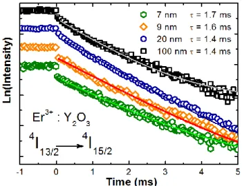
nm. The variation of luminescence lifetime of the 1.5 μm transition of Er3+ ions doped in films of different thicknesses and annealed at 950 °C is presented in Figure 10. Time-decay measurements confirmed that the ms long lifetime of the transition is preserved for low thicknesses down to 7 nm reflecting the small impact of the surface. Indeed quasi ex-ponential decays are observed with decay time constant of about 1.5 ms. These lifetime constants are shorter than the 7.7 ms measured for a 1 % Er doped Y2O3 transparent ceramic
but remain remarkably long in comparison to the values reported for 10 nm large nanocrystals (around 100 μs).57
10
Peak A Peak B
Samples Central frequency (GHz) inh (GHz) Central frequency (GHz) inh (GHz) 1% Eu:Y2O3 ceramic 516 098 24.2 - - 5% Eu:Y2O3 ceramic (extrapolated)53 - 97 - -
5% Eu:Y2O3 ALD thin film
annealed at 800°C
516 132 11 202 40 518 378 43 3608 157 5% Eu:Y2O3 ALD thin film
annealed at 900°C
516 182 3 240 10 518 211 27 2459 130 5% Eu:Y2O3 ALD thin film
annealed at 950°C
516 198 2 214 8 518 198 10 1982 110
Table 2 Central frequencies and inhomogenenous linewidth Γinh of peaks A and B reported in figure 8 as a function of the
an-nealing temperature. The extrapolated value for a 5% Eu doped ceramic annealed at 1200°C is added for comparison.
Figure 9 Inhomogeneous absorption line of the 7F0 → 5D0
transition of Eu3+ions in Y2O3 ALD thin films for different
annealing temperatures. Films are 168 nm thick and doped with 5 % Eu. Measurement temperature is 10 K. Emission of the 5D0 →
7
F2 transition is monitored at wavelengths above
610 nm as a function of the laser excitation frequency to probe the 7F0 →
5
D0 transition. The solid line is a fit of the
experimental points with two lorentzian line shapes. Curves have been vertically shifted for clarity.
Figure 10 Decay curves of the 1.5 μm fluorescence of Er3+ ions (2%) doped into ultra-thin Y2O3 films annealed at 950 °C.
Open scatter: experimental points, solid line: single exponen-tial fit. For clarity, curves have been vertically shifted.
In summary, we have optimized the growth of Eu and Er doped Y2O3 thin films by ALD and evaluated their optical
properties within the particular context of quantum technol-ogies. The possibility to produce this material system as thin films with a large range of compositions and doping indeed opens up new opportunities such as the coupling of emitters to resonators and hybrid structures as well as their spatial localization. The use of adapted growth conditions and post-growth thermal annealing confirmed that high quality ho-mogeneous films with narrow and well-resolved emission lines can be produced. Annealing temperatures on silicon were limited to about 950 °C in order to obtain the highest properties without the formation of parasitic silicate phases or cracks on the surface. Contamination by other RE ele-ments coming from the β-diketonate precursors were found and would probably require that higher purity or even spe-cially produced chemicals are used. As-grown ALD films were mostly of the cubic phase with a small contribution from a highly disordered monoclinic component leading to a different environment around the Eu3+ions. However, high temperature annealing led to an almost complete disappear-ance of the monoclinic residual phase and an improvement of the crystalline quality.
A detailed spectroscopic study of optimized 100 nm thick films showed that optical lifetime (T1) of the main 5D0 → 7F2
transition of Eu3+ions at 612 nm reached values of 0.8 ms close to that measured in transparent bulk ceramics. Besides the inhomogeneous linewidth Γinh of about 200 GHz was only
a factor of 2 higher than that expected from the bulk. It is also believed that lineshift of the emission is essentially re-lated to the tensile stress of 1 GPa induced by the post-treatment. Finally we demonstrated that the 1.5 μm telecom emission of Er3+ions can be observed in sub 10 nm-thick film grown under optimized conditions and post treatment with a lifetime as high as 1.7 ms.
The ability to synthesize films with such a low thickness is particularly relevant in the context of QTs where well-localized emitters are highly desirable. These optical proper-ties further establish RE3+:Y2O3 as a promising solid-state
nanoscale platform. It corroborates recent results obtained with nanoparticles that included a long optical coherence time (T2 > 10 μs) even for particles as small as 150 nm21,22,61 and
11
levels of Eu3+ions with ms-long coherence times.18Futurework will be dedicated to further harness the possibility of integrating ALD thin films into cavities to facilitate the ma-nipulation of emitters at the single ion level.
* E-mail: marion.scarafagio@chimieparistech.psl.eu;
alban.ferrier@chimieparistech.psl.eu
All authors have given approval to the final version of the manuscript.
This project has received funding from the European Union’s Horizon 2020 research and innovation programme under grant agreement No 712721 (NanOQTech).
The authors declare no competing financial interest.
(1) Liu, G.; Jacquier B. Spectroscopic Properties of Rare Earths in Optical Materials. Springer Series in Materials
Science 2005.
(2) Getz, M. N.; Hansen, P.-A.; Fjellvåg, Ø. S.; Ahmed, M. A. K.; Fjellvåg, H.; Nilsen, O. Intense NIR emission in YVO4:Yb3+ thin films by atomic layer deposition. J. Mater.
Chem. C 2017, 5, 8572-8578.
(3) Zhou, X.; Geng, W.; Guo, H.; Ding, J.; Wang, Y. K4CaGe3O9Mn2+,Yb3+: a novel orange-emitting
longper-sistent luminescent phosphor with a special nanostruc-ture. J. Mater. Chem. C 2018, 6, 7353-7360.
(4) Azimi, G.; Dhiman, R.; Kwon, H.-M.; Paxson A. T.; Vara-nasi, K. K. Hydrophobicity of rare-earth oxide ceramics.
Nature materials 2013, 12, 315-320.
(5) Liu, L.; Lei, J.; Li, L.; Zhang, J.; Shang, B.; He, J.; Li N.; Pan F. Robust Rare-Earth-Containing Superhydrophobic Coatings for Strong Protection of Magnesium and Alu-minum Alloys. Adv. Mater. Interfaces 2018, 5, 1800213. (6) Trovarelli, A. Catalytic Properties of Ceria and CeO2
-Containing Materials. Catalysis review 1996, 38:4, 439-520.
(7) Ma, H. J.; Jung, W. K.; Park Y.; Kim, D. K. A novel ap-proach of an infrared transparent Er:Y2O3-MgO
nano-composite for eye-safe laser ceramics. J. Mater. Chem. C
2018, 6, 11096-11103.
(8) Leskela, M.; Kukli K.; Ritala, M. Rare-earth oxide thin films for gate dielectrics in microelectronics. Journal of
Alloys and Compounds 2006, 418, 27-34.
(9) Fanciulli M.; Scarel, G. Rare Earth Oxide Thin Films.
Springer series in Topics in applied science 2007.
(10) Goldner, P.; Ferrier A.; Guillot-Noël, O. Handbook on the Physics and Chemistry of Rare Earths 2015, 46, 1-78. (11) Equall, R. W.; Sun Y.; Cone, R. L. Ultraslow Optical
Dephasing in Eu3+:Y2SiO5. Phys. Rev. Lett. 1994, 72,
2179-2182.
(12) Zhong, M.; Hedges, M. P.; Ahlefeldt, R. L.; Bartholomew, J. G.; Beavan, S. E.; Wittig, S. M.; Longdell, J. J.; Sellars, M. J. Optically addressable nuclear spins in a solid with a six-hour coherence time. Nature 2015, 517, 177-181. (13) Laplane, C.; Jobez, P.; Etesse, J.; Gisin, N.; Afzelius, M.
Multimode and Long-Lived Quantum Correlations
Be-tween Photons and Spins in a Crystal. Phys. Rev. Lett.
2017, 118, 210501.
(14) Clausen, C.; Usmani, I.; Bussières, F.; Sangouard, N.; Afzelius, M.; de Riedmatten, H.; Gisin, N. Quantum stor-age of photonic entanglement in a crystal. Nature 2011,
469, 508-512.
(15) Bussières, F.; Clausen, C.; Tiranov, A.; Korzh, B.; Verma, V. B.; Nam, S. W.; Marsili, F.; Ferrier, A.; Goldner, P.; Herrmann, H. et al. Quantum teleportation from a telacom-wavelength photon to a solid-state quantum memory Nature Photonics 2014, 8, 775.
(16) Zhong, T.; Kindem, J. M.; Bartholomew, J. G.; Rochman, J.; Craiciu, I.; Miyazono, E.; Bettinelli, M.; Cavalli, E.; Verma, V.; Nam, S. W. et al. Nanophotonic rare–earth quantum memory with optically controlled retrieval.
Science 2017, 357, 1392-1395.
(17) Dibos, A. M.; Raha, M.; Phenicie, C. M.; Thompson, J. D. Atomic Source of Single Photons in the Telecom Band
Phys. Rev. Lett. 2018, 120, 243601.
(18) Serrano, D.; Karlsson, J.; Fossati, A.; Ferrier, A.; Goldner, P. All-optical control of long-lived nuclear spins in rare-earth doped nanoparticles Nature Communications 2018,
9, 2127.
(19) Casabone, B.; Benedikter, J.; Hümmer, T.; Oehl, F.; de Oliveira Lima, K.; Hänsch, T. W.; Ferrier, A.; Goldner, P.; de Riedmatten, H.; Hunger, D. Cavity-enhanced spec-troscopy of a few-ion ensemble in Eu3+:Y2O3. New J. Phys. 2018, 20, 095006.
(20) O’brien, J. L.; Furusawa, A.; Vučković, J. Photonic quan-tume technologies. Nature Photonics 2010, 3, 687. (21) Perrot, A.; Goldner, P.; Giaume, D.; Lovrić, M.;
Andri-amiadamanana, C.; Gonçalves, R. R.; Ferrier, A. Narrow Optical Homogeneous Linewidths in Rare Earth Doped Nanocrystals. Phys. Rev. Lett. 2013, 111, 203601.
(22) Bartholomew, J. G.; de Oliveira Lima, K.; Ferrier, A.; Goldner, P. Optical Line Width Broadening Mechanisms at the 10 kHz Level in Eu3+:Y2O3 Nanoparticles NanoLett. 2017, 17, 778-787.
(23) Tielrooij, K. J.; Orona, L.; Ferrier, A.; Badioli, M.; Navick-aite, G.; Coop, S.; Nanot, S.; Kalinic, B.; Cesca, T.; Gau-dreau, L. et al. Electrical control of optical emitter relaxa-tion pathways enabled by graphene. Nature Physics 2015,
11, 281.
(24) Pons-Y-Moll, O.; Perriere, J.; Millon, E.; Defourneau, R. M.; Defourneau, D.; Vincent, B.; Essahlaoui, A.; Bou-drioua, A.; Seiler, W. Structural and optical properties of rare-earth-doped Y2O3 waveguides grown by pulsed-laser
deposition. J. Appl. Phys. 2002, 92, 4885.
(25) Schulz, U.; Fritscher, K.; Peters, M. EB-PVD Y2O3- and
CeO2/Y2O3-stabilized zirconia thermal barrier coatings –
crystal habit and phase composition. Surface and
Coat-ings Technology 1996, 82, 259-269.
(26) Miikkulainen, V.; Leskel, M.; Ritala, M.; Puurunen, R. L. Cristallinity of inorganic films grown by atomic layer deposition: Overview and general trends J. Appl. Phys.
2013, 113, 021301 and reference therein.
(27) Park, I.-S.; Jung, Y. C.; Seong, S.; Ahn, J.; Kang, J.; Noh, W.; Lansalot-Matras, C. Atomic layer deposition of Y2O3
films using hetroleptic liquid (iPrCp)2Y(iPr-amd)
precur-sor J. Mater. Chem. C 2014, 2, 9240-9247.
(28) Shen, T.; Li. R.; Sun, M.; Pan, D.; Zhang, J.; Xu, J.; Zhao, J.; Chen, Q. Improving the electrical properties of InAs nanowire field effect transistors by covering them with Y2O3/HfO2 layers. Nanoscale 2018, 10, 18492-18501.
(29) West, G. A.; Beeson, K. W. Low-pressure metalorganic chemical vapor deposition of photoluminescent Eu-doped Y2O3 films. Journal of Materials Research 1990, 5,
1573-1580.
(30) Dimoulas, A.; Travlos, A.; Vellianitis, G.; Boukos N.; Argyropoulos, K. Direct heteroepitaxy of crystalline Y2O3
on Si(100) for high-k gate dielectric applications. J. Appl.
12
(31) Ioannou-Sougleridis, V.; Constantoudis, V.; Alexe, M.; Scholz, R.; Vellianitis G.; Dimoulas, A. Effects on surface morphology of epitaxial Y2O3 layers on Si(100) after
post-growth annealing. Thin Solid Films 2004, 468, 303-309. (32) Hoang, J.; Schwartz, R. N.; Wang, K. L.; Chang, J. P. The
effects of energy transfer on the Er3+ 1.54 mu m lumines-cence in nanostructured Y2O3 thin films with
heteroge-neously distributed Yb3+ and Er3+ codopants. J. Appl.
Phys. 2012, 112, 063117.
(33) Van, T. T.; Chang, J. P. Controlled erbium incorporation and photoluminescence of Er-doped Y2O3. Applied
Phys-ics Letters 2005, 87, 011907.
(34) Barth, J.; Johnson, R. L.; Cardona, M.; Palik, E. D. Hand-book of optical constants of solids II. Academic Press,
New York 1991.
(35) Adachi, G.-Y.; Imanaka, N. The Binary Rare Earth Oxides
Chem. Rev. 1998, 98, 1479-1514.
(36) Dexpert-Ghys, J.; Faucher, M.; Caro, P. Site-selective excitation, crystal-field analysis, and energy transfer in europium-doped monoclinic gadolinium sesquioxide. A test of the electrostatic model. Phys. Rev. B 1981, 23, 607. (37) de Oliveira Lima, K.; Gonçalves, R. R.; Giaume, D.;
Ferri-er, A.; GoldnFerri-er, P. Influence of defects on sub-Å optical linewidths in Eu3+: Y2O3 particles. Journal of
Lumines-cence 2015, 168, 276-282.
(38) Putkonen, M.; Sajavaara, T.; Johansson, L.-S.; Niinistö, L. Low-Temperature ALE Deposition of Y2O3 Thin Films
from β-Diketonate Precursors. Chem. Vap. Deposition
2001, 7, 44.
(39) Quah, H. J.; Cheong, K. Y. Effects of post-deposition annealing ambient on Y2O3 gate deposited on silicon by
RF magnetron sputtering. Journal of Alloys and
Com-pounds 2012, 529, 73-78.
(40) Richardson, F. S. Terbium(III) and Europium(III) Ions as Luminescent Probes and Stains for Biomolecular Sys-tems. Chem. Rev. 1982, 82, 541-552.
(41) Li, Z.; Wang, J.; Hou, Y.; Bai, X.; Song, H.; Zhou, Q.; Wei, T.; Li, Y.; Liu, B. Analysis of the upconversion photolu-minescence spectra as a probe of local microstructure in Y2O3/Eu3+ nanotubes under high pressure. RSC Adv. 2015,
5, 3130.
(42) Zhang, J.; Cui, H.; Zhu, P.; Ma, C.; Wu, X.; Zhu, H.; Ma, Y.; Cui, Q. Photoluminescence studies of Y2O3:Eu3+ under
high pressure. J. Appl. Phys. 2014, 115, 023502.
(43) Karaveli, S.; Weinstein, A. J.; Zia, R. Direct Modulation of Lanthanide Emission at Sub-Lifetime Scales. NanoLett.
2013, 13, 2264-2269.
(44) Rubio, E. J.; Atuchin, V. V.; Kruchinin V. N.; Pokrovsky, L. D.; Prosvirin, I. P.; Ramana, C. V. Electronic Structure and Optical Quality of Nanocrystalline Y2O3 Film
Surfac-es and InterfacSurfac-es on Silicon. J. Phys. Chem. C 2014, 118, 13644 – 13651.
(45) Hua, C.; Chen, L.; Li, C.; Wang, M.; Guo, J.; Liu, J.; Yan, X.; Zhao, Y.; An, K.; Wei, J. et al. Effects of oxygen-to-argon ratio on crystalline structure and properties of Y2O3 anti-reflaction films for freestanding CVD diamond.
Journal of Alloys and Compounds 2017, 693, 468-473.
(46) Yang, H.-S.; Hong, K. S.; Feofilov, S. P.; Tissue, B. M.; Meltzer, R. S.; Dennis, W. M. Electron-phonon interac-tion in rare earth doped nanocrystals. Journal of
Lumi-nescence 1991, 83-84, 139-145.
(47) Williams, D. K.; Bihari, B.; Tissue, B. M.; McHale, J. M. Preparation and Fluorescence Spectroscopy of Bulk Monoclinic Eu3+:Y2O3 and Comparison to Eu3+:Y2O3
Nanocrystals. J. Phys. Chem. B 1998, 102, 916.
(48) Ferrier, A.; Ilas, S.; Goldner, P.; Louchet-Chauvet, A. Scandium doped Tm:YAG ceramics and single crystals: Coherent and high resolution spectroscopy. Journal of
Luminescence 2018, 194, 116.
(49) Babbitt, W. R.; Lezama, A.; Mossberg, T. W. Optical dephasing, hyperfine structure, and hyperfine relaxation
associated with the 580.8-nm 7F
0-5D0 transition of
euro-pium in Eu3+:Y
2O3. Phys. Rev. B 1989, 39, 1987.
(50) Ferrier, A.; Thiel, C. W.; Tumino, B.; Ramirez, M. O.; Bausa, L. E.; Cone, R. L.; Ikesue, A.; Goldner, P. Narrow inhomogeneous and homogeneous optical linewidths in a rare earth doped transparent ceramic. Phys. Rev. B
2013, 87, 041102.
(51) Kushida, T.; Tanaka, M. Transition mechanisms and spectral shapes of the 5D0-7F0 line of Eu3+ and Sm2+ in
sol-ids. Phys. Rev. B 2002, 65, 195118.
(52) Stoneham, A. M. Shapes of Inhomogeneously Broadened Resonance Lines in Solids. Rev. Mod. Phys. 1969, 41, 82. (53) Kunkel, N.; Ferrier, A.; Thiel, C. W.; Ramirez, M. O.;
Bausa, L. E.; Cone, R. L.; Ikesue, A.; Goldner, P. Rare-earth doped transparent ceramics for spectral filtering and quantum information processing. APL Materials
2015, 3, 096103.
(54) Ylivaara, O. M. E.; Liu, X.; Kilpi, L.; Lyytinen, J.; Schnei-der, D.; Laitinen, M.; Julin, J.; Ali, S.; Sintonen, S.; Berdo-va, M. et al. Aluminum oxide from trimethylaluminum and water by atomic layer deposition: The temperature dependence of residual stress, elastic modulus, hardness and adhesion. Thin Solid Films 2014, 552, 124-135.
(55) Palko, J. W.; Kriven, W. M.; Sinogeikin, S. V.; Bass, J. D.; Sayir, A. Elastic constants of yttria (Y2O3) monocrystals
to high temperatures. J. Appl. Physics 2001, 89, 7791. (56) Yim, W. M.; Paff, R. J. Thermal expansion of AIN,
sap-phire, and silicon. J. Appl. Physics 1974, 45, 1456.
(57) Dorman, J. A.; Choi, J. H.; Kuzmanich, G.; Chang, J. P. Elucidating the Effects of a Rare-Earth Oxide Shell on the Luminescence Dynamics of Er3+:Y2O3 Nanoparticles. J.
Phys. Chem. C 2012, 116, 10333-10340.
(58) Polman, A. Erbium as a probe of everything? Physica B
2001, 300, 78-90.
(59) Slooff, L. H.; van Blaaderen, A.; Polman, A.; Hebbink, G. A.; Klink, S. I.; Van Veggel, F. C. J. M.; Reinhoudt, D. N.; Hofstraat, J. W. Rare-earth doped polymers for planar optical amplifiers. J. Appl. Physics 2002, 91, 3955.
(60) Proslier, T.; Becker, N. G.; Pellin, M. J.; Klug J.; Elam, J.W. Controlling the emissive properties of materials-improved lasers and upconversion materials. Patent US
8,518,179 B1 2013.
(61) Liu, S.; Serrano, D.; Fossati, A.; Tallaire, A.; Ferrier, A.; Goldner, P. Controlled size reduction of rare earth doped nanoparticles for optical quantum technologies. RSC