HAL Id: hal-02999606
https://hal.archives-ouvertes.fr/hal-02999606
Submitted on 10 Nov 2020HAL is a multi-disciplinary open access archive for the deposit and dissemination of sci-entific research documents, whether they are pub-lished or not. The documents may come from teaching and research institutions in France or abroad, or from public or private research centers.
L’archive ouverte pluridisciplinaire HAL, est destinée au dépôt et à la diffusion de documents scientifiques de niveau recherche, publiés ou non, émanant des établissements d’enseignement et de recherche français ou étrangers, des laboratoires publics ou privés.
UV nanophotodetectors: A case study of individual
Au-modified ZnO nanowires
Oleg Lupan, Vasile Postica, Thierry Pauporté, Mathias Hoppe, Rainer
Adelung
To cite this version:
Oleg Lupan, Vasile Postica, Thierry Pauporté, Mathias Hoppe, Rainer Adelung. UV nanophotode-tectors: A case study of individual Au-modified ZnO nanowires. Sensors and Actuators A: Physical , Elsevier, 2019, 296, pp.400 - 408. �10.1016/j.sna.2019.07.040�. �hal-02999606�
1 Please cite this article as:
Oleg Lupan,1,2,3,* Vasile Postica,2 Thierry Pauporté,3 Mathias Hoppe,1 Rainer Adelung,1
UV nanophotodetectors: A case study of individual Au-modified ZnO
nanowires
Sensors and Actuators A 296 (2019) 400–408. DOI: 10.1016/j.sna.2019.07.040
1 Functional Nanomaterials, Faculty of Engineering, Institute for Materials Science, Kiel University,
Kaiserstr. 2, D-24143, Kiel, Germany
2 Department of Microelectronics and Biomedical Engineering, Technical University of Moldova, 168
Stefan cel Mare Av., MD-2004 Chisinau, Republic of Moldova
3 PSL Université, Institut de Recherche de Chimie Paris, ChmieParisTech, UMR CNRS 8247, 11 rue
Pierre et Marie Curie 75231 Paris cedex 05, France *Corresponding authors
Prof. Dr. Eng. Lupan, Prof. Dr. Adelung E-mails: ollu@tf.uni-kiel.de ra@tf.uni-kiel.de
Institute for Materials Science, Kiel University, Germany
2
Abstract
In this work, ultraviolet (UV) nanophotodetectors based on individual gold-functionalized ZnO nanowires (Au/ZnO NWs) with different diameters and with different Au content were fabricated using a focused ion beam/scanning electron microscopy (FIB/SEM) system. The influence of the Au content, the diameter of the NWs, the applied bias voltage, the temperature and the relative humidity during operation on the UV sensing properties was investigated in detail. The necessity of a higher Au nanoparticles (NPs) coverage of individual Au/ZnO NWs in order to obtain higher UV response is demonstrated for the first time. A high UV response (IUV/Idark) of 21
for an individual Au/ZnO NW (with ~ 6.4% Au NPs coverage) was obtained, which is by a factor of 17 higher compared to unmodified ZnO NWs. The investigation regarding the NW diameter confirmed that thinner NWs are more suitable for UV sensing applications due to the greater influence of surface phenomena on electrical properties. Most importantly, the elaborated nanophotodetectors in this work, based on individual Au/ZnO NWs, show an extreme low influence caused by water vapors, i.e. relative humidity on UV response, which is critical for practical applications of high performance UV photodetectors in normal ambient conditions. Our experimental results demonstrate clearly that the n-type Au/ZnO NWs with enhanced optoelectronic properties are highly promising building blocks for near future nano-optoelectronic devices and possible for biosensing applications.
1. Introduction
One-dimensional (1-D) ZnO nanostructures, such as nanowires, nanobelts, nanotubes and nanorods are ideal for building blocks for high-performance electronic, optoelectronic and sensing devices for environmental applications [1-9]. In the case of sensing devices (e.g. UV photodetectors and gas sensors) the high influence of surface phenomena, such as
3
adsorption/desorption of gaseous species on the electrical transport through a restricted conduction channel of 1-D nanostructures paves the way to fabricate highly sensitive UV photodetectors and gas sensors based on individual nanostructures [3, 7, 8, 10-15]. The main advantage of UV photodetectors based on individual ZnO NWs is the high internal gain, which is attributed to the presence of oxygen-related hole-trap states at the NW surface which prevents charge-carrier recombination through prolongation of the photo-carrier lifetime [16].
Different methods were reported in order to considerably enhance the UV sensing properties of individual ZnO NWs, such as doping [11], surface functionalization with noble metals [3], formation of individual Schottky contacts at one end of the NW [6], as well as functionalization with other metal oxide NPs [13], and the utilization of the piezo-phototronic effect [17]. For example, Hu et al. fabricated UV photodetectors based on a ZnS/ZnO biaxial nanobelt with high spectral selectivity and wide-range photoresponse in the UV-A band [18]. Lao
et al. demonstrated that the UV response of individual ZnO nanobelts can be enhanced by almost
5 orders of magnitude by surface functionalizing with a polymer that has a high UV absorption ability [19]. While the UV sensing properties of photodetectors based on Au-modified ZnO micro- and nanostructures have been reported many works [20, 21], only the several results were reported based on individual Au-modified ZnO structures [3, 22]. For example, Liu et al. fabricated the UV photodetectors based on an individual ZnO NW with and without Au NPs and observed that surface-functionalization with Au NPs can drastically reduce the response time of ZnO nanowire photodetectors [3].
However, the interdependence of such important parameters as surface coverage with Au NPs and the diameter of the ZnO NW, relative humidity, applied bias and operation temperature were not investigated and reported. In this work, we integrated individual Au-modified ZnO NWs with different Au content and different diameters using a dual beam FIB/SEM system. The Au/ZnO NWs were synthesized in a one-step electrochemical deposition [23]. Besides the report
4
about the influence of the already enumerated factors, i.e. diameter, relative humidity, applied bias voltage and temperature for a single Au/ZnO NWs based device, the corresponding physical model and the mechanism of detection are tentatively proposed and discussed.
2. Experimental part
The Au/ZnO NW arrays were grown on glass sheet substrates coated with polycrystalline F-doped SnO2 (FTO) having a resistance of 10 Ω/ (used as a working electrode) by
electrochemical deposition in a classical three-electrode electrochemical cell [11, 24]. The growth solution contained 0.2 mM ZnCl2, 0.1 M KCl as supporting electrolyte and was subjected to
continuous bubbling of oxygen in a bath solution [24, 25]. For variation of Au NPs content on the surface of ZnO NWs, different concentrations of HAuCl4 (Sigma-Aldrich, >99.9%) were utilized
(from 0.3 to 2.0 μM). Upon deposition, the substrate was rotated at a constant speed of ω = 300 rotations/min (rpm) [11, 24]. More details on the electrochemical deposition of doped ZnO NWs are presented in previous works [11, 24, 26]. The detailed morphological, structural, chemical and optical properties of Au/ZnO NW arrays were performed in the previous work [23] and indicated that Au ions are not incorporated in the ZnO matrix (i.e. no doping was observed or proved) but Au agglomerations are deposited on the surface of the ZnO NWs in the form of nanoclusters with a diameter in the range of 20 – 50 nm [23]. In other words, the growth and surface functionalization of ZnO NWs with Au nanoparticles is performed with the same electrochemical deposition process, which is an important advantage because it allows to cut down additional technological steps for post-growth surface functionalization [23].
The nanophotodetectors based on individual ZnO:Au NWs were fabricated using the method developed by Lupan et al. in a dual beam FIB/SEM scientific instrument [11, 23, 27, 28]. The UV sensing measurements were performed at room temperature (RT, ~ 25 ºC) in normal
5
ambient air (relative humidity, RH ~ 20%). The UV light irradiance (λ = 365 nm) was set to ~ 1 mW/cm2.
3. Results and discussions
3.1. Nanophotodetectors based on an individual Au/ZnO NW. Influence of Au NPs coverage
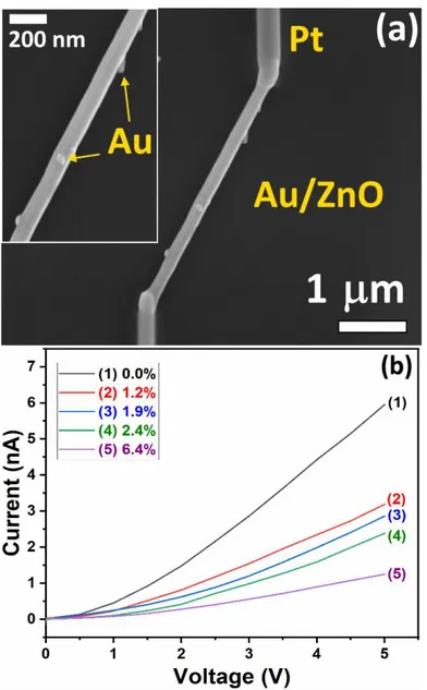
A typical SEM image of a nanophotodetectors fabricated using an individual Au/ZnO nanowire is presented in Figure 1a. The individual Au/ZnO NW, which is placed on SiO2/Si
substrate, is connected to Au/Cr electrodes using two Pt contacts. The current – voltage (I–V) characteristics of individual ZnO NWs with different Au NPs coverage (determined from SEM images of the devices and calculated by (SNP · 100%)/SNW, where SNP is the Schottky contact area formed by Au NPs (πr2, where r is the Au NPs radius) and SNW is the surface of the ZnO NWs (2πrh, where r and h are the radius and length of the NW) and with a 120 ± 10 nm diameter is presented in Figure 1b. The I–V measurements clearly show a resistance decrease of the devices with higher Au coverage. This can be attributed to the formation of the larger Schottky contact area, and respectively to the more narrowed conduction channel [3, 20, 29].
Figure 2a shows the room temperature UV photoresponse for individual Au/ZnO NWs
with different Au NP coverage (determined from SEM images of the devices and calculated by (SNP · 100%)/SNW, where SNP is the Schottky contact area formed by AuNPs (πr2, where r is the Au NPs radius) and SNW is the surface of the ZnO NWs (2πrLNW, where rNW and LNW are the radius
and length of the NW)). The measurements were performed under 2 V bias voltage applied to the individual Au/ZnO NW. The SEM images of the nanodevices are shown in our previous work [23]. The content of Au NPs was mainly varied using different concentrations of HAuCl4 in the
electrolyte solution. From a previous work it was observed that by increasing the HAuCl4 from
6
[23]. However, in the Au/ZnO NW arrays grown using the same content of HAuCl4 (for example
0.9 μM), the Au/ZnO NW with a large variation of Au NPs on the surface can be found (even without Au NPs) [23]. Therefore, the number of Au NPs on the integrated individual Au/ZnO NW depends more on the chosen NW for integration, than on the HAuCl4 content used for growth of
these NWs. This is the reason why the UV response was plotted against the Au NPs coverage and not against the HAuCl4 concentration used for growth of Au/ZnO NWs.
The UV response for Au NPs coverage of 0, ~ 1.2, ~ 1.5, ~ 3.5 and ~ 6.4 % is ~ 1.2, ~ 2.75, ~ 5, ~ 9 and ~ 21, respectively. As can be observed, the UV response increases with Au NPs coverage. Because the diameter of all NWs is about 120 ± 10 nm, the surface of the formed Schottky contacts at the Au/ZnO interface plays an important role for the determination of the device parameters [4, 20]. Thus, by increasing the surface of the Schottky contact, the higher influence of surface phenomena on the charge transport of an individual Au/ZnO NW can be achieved [30, 31].
Figure 2b shows the dynamic response to UV light of Au/ZnO NWs without Au NPs on
the surface and with ~ 1.2% and ~ 6.4% Au NPs coverage. The rise and decay time constants of the photocurrent are determined through a bi-exponential fit respectively from the corresponding time-resolved measurements, as was reported previously [32]:
− + − + = 1 − 1 1 − 2 ) ( 1 r 2 r t t dark A e A e I t I (1) 2 1 4 3 ) ( d d t t dark Ae Ae I t I − − + + = (2)
where A1, A2, A3 and A4 are positive constants. τr1, τr2 and τd1, τd2 are time constants for rising and
decaying of the photocurrent, respectively. The results of the curve fittings are presented in Figure
2c. τr1 and τd1 are correlated to the rapid concentration change of the charge carriers when the UV
7
vacancies of oxygen defects in the thin film, as well as photodesorption/adsorption of oxygen molecules, which are in comparison much slower processes [33-35]. From Figure 2c it can be observed that by an increase in Au NP coverage of individual Au/ZnO NWs, the time constants of rising and decaying photocurrents are considerably decreased. This is more observable from
Figure S1a, where the normalized UV response of Au/ZnO NWs from Figure 2b is presented. In
the case of individual NWs without Au NPs and ~ 1.2% coverage a relatively low signal to noise ratio (SNR) can be observed. According to IUPAC definition, the signal is considered to be true if the SNR > 3 [36]. The SNR was defined as IUV −Idark /, where σ is the standard deviation of the current before illumination with UV light. The SNR for an individual Au/ZnO NW without Au NPs, with ~ 1.2 and ~ 6.4 % coverage is 11.49, 7.28 and 6.77, respectively, confirming that the signal is true.
The improved UV sensing properties of individual Au/ZnO NWs compared to a ZnO NW can be explained as follows. The UV sensing performances of micro- and nanostructures of metal oxides depend on electron – hole (e––h+) pairs generation and surface processes, such as adsorption/photodesorption of oxygen molecules [15, 37, 38]. In the dark, oxygen molecules (O2) are adsorbed on the surface of the ZnO NW by capturing free electrons (O2 + e– → O2–) [3, 39,
40]. In result, a surface electron depletion region (Ldark) is formed with a higher resistivity compared to the conduction channel (ddark, see Figure 2d). In this case, the electrical conductance of the ZnO NW (G) is given by [41]:
NW dark NW L L r n q G 2 0 − = (3)where q is the electron charge, n0 is the concentration of free electrons and µ is the electron mobility.
Under UV illumination, e––h+ pairs are photogenerated [11]. While the e– increases the photocurrent through the conduction channel of the NW, the h+ migrates to the ZnO surface and
8
discharges O2– by surface electron-hole recombination (h+ + O2– → O2), which leads to the narrowing of the surface electron depletion region (LUV) and a widening of the conduction channel (dUV, see Figure 2f) [11, 16]. The photoresponse in a steady state (ΔGph, when recombination and
generation rates (g) are equal) is given by [41]:
surf bulk ph g p n G 1/ / 1 + = = (4)
where Δn and Δp are the excess numbers of n and p carriers, and
τ
bulk andτ
surf are the lifetimes ofthe photocarriers recombined in the bulk and at the surface.
In the case of Au/ZnO NWs, the presence of Au NPs on the surface leads to a formation of Schottky barriers at the Au/ZnO NW interface due to a higher work function of Au (φAu = 5.1 eV) compared to those of ZnO (φAu = 4.1 eV) (see Figure 2e) [3, 42]. This results in a much more narrowed conduction channel of the Au/ZnO NW, and a lower dark current, which was observed in Figure 1b [3, 11, 16]. Under UV illumination, the photogenerated holes will migrate to the Au NPs due to the interactive Coulomb force [3]. Some of the holes are trapped at the Au-ZnO interface and some of the holes pass through the Schottky barrier at the interface, where the electron-hole recombination will induce a reduction of the Schottky barrier and a narrowing of the electron depletion region, respectively (Figure 2g) [3]. Also, the presence of Au NPs can improve the light absorption efficiencyby particle-induced light scattering, i.e. increasing the number of photogenerated e––h+ pairs [43], as well as increase the lifetime of photogenerated carriers and therefore the photoresponse by the increasing in the efficiency of charge carrier separation (see eq. (4)) [41, 44]. Therefore, the particle-induced scattering and Au/ZnO Schottky barriers can be responsible for the great enhancement of UV sensing properties of an individual Au/ZnO NW-based nanophotodetector [3].
9
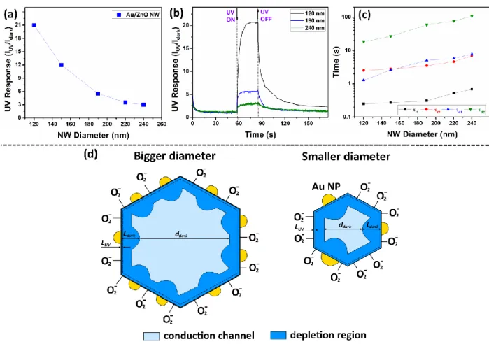
The sensing mechanism of individual ZnO micro- and nanostructures is primarily surface related, therefore surface states, oxygen adsorption quantities and the diameter play important roles on the UV sensitivity [3, 45], the influence of the latter for an individual Au/ZnO NW was also investigated. Figure 3a shows the room temperature UV response of a Au/ZnO NW (with ~ 6.4% coverage) versus the diameter. The measurements were performed with 2 V bias voltage. The UV response for Au/ZnO NWs with individual diameters of 120, 150, 190, 220 and 240 nm is ~ 21, ~ 12, ~ 5.5, ~ 3.5 and ~ 3, respectively. The results show a considerable decrease in the UV response with the NW diameter enlargement from 120 to 240 nm. The dynamic responses for NWs with 120, 190 and 240 nm are presented in Figure 3b. The calculated time constants for rising and decaying of the photocurrent in dependence of the NW diameter are presented in Figure 3c. As can be observed, the recovery of the photocurrent is found to be strongly related to the diameter of NWs, which is more observable from Figure 3d.
The size-dependent UV sensing properties of individual nanostructures were observed by several authors [46-50]. The decrease in response by a widening of the diameter of the NW can be explained based on a reduced influence of surface phenomena on the conductive channel of the NW (see Figure 3e). Chen et al. demonstrated that the recovery of the photocurrent for an individual ZnO NW is found to be strongly related to the diameter of NWs, indicating that the photocarrier relaxation behavior is dominated by surface band bending [48]. It can explain the observed data from Figure 3c, i.e. dependence of the time constants for rising and decaying photocurrents.
3.3. Influence of the operating temperature and the applied bias voltage on sensing
performances
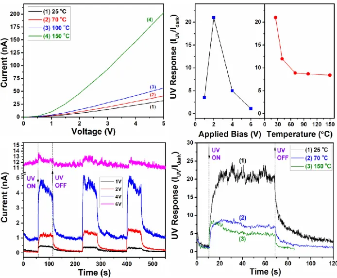
Next, the influence of the operating temperature and the applied bias on the UV sensing properties is investigated. Figure 4a shows the current – voltage (I-V) characteristic of individual
10
Au/ZnO NWs (with ~ 6.4% coverage) with a diameter of 120 nm at different operating temperatures (25, 70, 100 and 150 ºC). A typical semiconductor I-V characteristic, i.e. increasing of the current value at higher temperatures due to thermal activation of the charge carriers [2, 8], is found. The dependence of the UV response on the applied bias and operating temperature is presented in Figure 4b. It is observed that the highest UV response is obtained at 2 V (~ 21), while a further increase in bias voltage to 4 V and 6 V leads to a response decrease to 5 and 1.1, respectively. At an applied bias voltage of 1 V the UV response is much lower, ~ 3.5. Increasing the operating temperature reduces the UV response (see Figure 4b). The UV response at 25, 40, 70, 100 and 150 ºC is ~ 21, ~ 12, ~ 8.9, ~ 8.7 and ~ 8.4, respectively. The dynamic response of individual Au/ZnO NWs with a diameter of 120 nm at different applied bias voltages and different operating temperatures (25, 70 and 150 ºC) is presented in Figure 4c and 4d, respectively.
The reduction in the UV sensing performance at elevated operating temperatures can be explained mainly by the higher dark current due to an enhancement in tunneling currents [51] and the increased probability of recombination of photogenerated e− – h+ pairs [52]. The decreasing in the UV response by increasing applied bias voltages can be explained based on the well-known self-heating effect [53, 54]. Therefore, the higher the applied bias, the more heat will be generated by Joule dissipation [41]. Strelcov et al. assumed that the temperature of the self-heated suspended NW has a linear gradient from highest temperature in the center to the ambient temperature at the electrical leads and that the Joule power, generated in such a NW, is dissipated via three channels: heat transfer to the ambient gas, to the metal contacts and via radiation losses [54]. However, in our case the Au/ZnO NWs are placed on SiO2 (300 nm)/Si substrates, and a part of the temperature
is dissipated through this substrate.
As a future perspective, the self-heating effect by Joule dissipation could be improved using suspended NWs.
11
3.4. Influence of the relative humidity on sensing performances
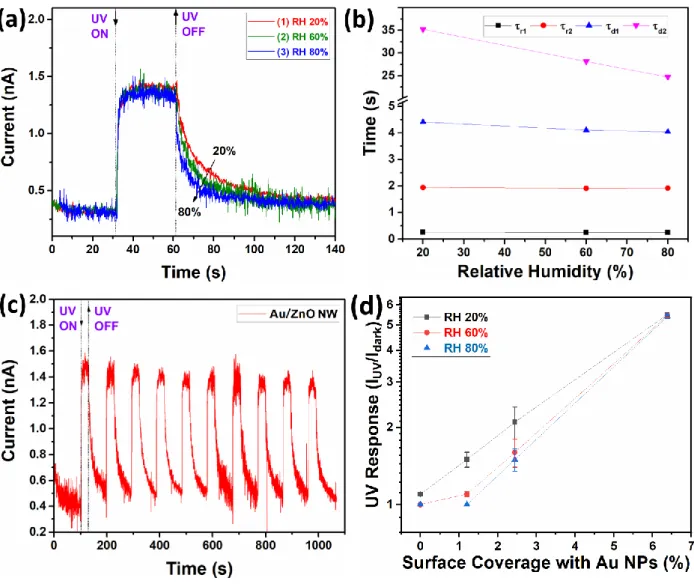
Because the UV sensing properties of UV photodetectors, such as the UV response and the time constants (response/recovery), are dominated by surface phenomena/processes involving adsorption/desorption of oxygen species, other chemical species in the environment reduce or increase the response/recovery time [55]. In particular, water molecules are present in high quantities in the environment and can affect the sensing performances of ZnO micro- and nanostructures. It remains a serious limitation for practical photosensing applications [35, 55, 56]. Therefore, without surface passivation the effect of water vapors is hard to avoid. In this context, the humidity influence on UV sensing properties of individual ZnO nanostructures was less reported [57].
Our previous measurements were performed at a normal ambient RH of ~ 20% and we also performed UV sensing measurements at higher values of RH of ~ 60% and ~ 80% at room temperature. Results of an individual Au/ZnO NW with a diameter of 190 nm are presented in
Figure 5a. The data are presented using the measured current, in order to better demonstrate the
influence of the modified RH on the dark current. Neither essential changes in dark currents nor in the value of the UV response were visible with the RH value. The calculated time constants for the rising and decaying photocurrent in dependence of the RH are presented in Figure 5b. The time constants for the rising photocurrent show no essential changes, while in the case of the time constants for the decaying photocurrent a slight decrease in the values can be observed. The dynamic response to multiple pulses at 80% RH is presented in Figure 5c, in order to demonstrate the good repeatability even at high values of RH. Figure 5d shows the UV response at different values of RH (20, 60 and 90%) for an individual Au/ZnO NW with diameter of 190 nm and with a different Au NPs coverage on the surface. The results clearly demonstrate that a lower coverage with Au NPs leads to a higher dependence of the UV response on the RH.
12
The low impact of water vapors on the UV sensing properties of an individual Au/ZnO NW can be explained as follows. In presence of water vapors the current level in the dark is slightly increased and under illumination significantly decreased [56]. These current modifications are attributed to the adsorption of water molecules (H2O) on the surface of ZnO by generation of free
electrons [35, 58]:
(
−)
+ ••+ − + +O Zn OH Zn V e O H2 O 2 Zn 2 O 2 (3)where VO•• is the vacancy created at an oxygen site, OO is the oxygen atom from the lattice and
ZnZn is the zinc atom from the lattice. Therefore, by increasing the concentration of water
molecules, more adsorption sites on the ZnO NW surface are occupied by hydroxyl groups and increase the value of the dark current by narrowing the width of the electron depletion region [35, 58, 59]. This reduces the lifetime of photogenerated carriers leading to a lower photocurrent [35, 58, 59]. More details about the mechanism are presented in our previous work [35]. However, in our case the lack of changes in the dark- and photocurrent may indicate on that Au NPs act as hydroxyl adsorbers on the surface of NPs, thereby providing an oxygen adsorption site for surface reactions in a humid atmosphere [60]. The same effect was observed for NiO-doped SnO2 [61],
Sb-doped SnO2 [62], CuO-loaded SnO2 hollow spheres [63], Al-doped SnO2 NPs [60] and Fe2O3
-functionalized ZnO tetrapods [13].
Figure 6 shows the schematic model of hydroxyl and oxygen co-adsorption on the surface
of ZnO and Au/ZnO NW. In the presence of humidity the hydroxyl groups are adsorbed on the surface of the ZnO NW resulting in width changes of the conduction channel Lair (see Figure
6a,b). By the increase in concentration of water vapors, the adsorption of oxygen species is highly
decreased due to hydroxyl poisoning, which was confirmed by other investigations [60, 61], and extends the width of the conduction channel (Lair+RH, see Figure 6a,b). Thus, less photogenerated holes under UV illumination will migrate to the ZnO surface to discharge O2– by surface
electron-13
hole recombination, leading to the lowering in modulation of the conduction channel and respectively to lowering in the UV response (see Figure 6c) [11, 16].
In the case of a Au/ZnO NW (see Figure 6d,e), the hydroxyl groups are adsorbed mainly on the surface of Au NPs, maintaining the adsorption of O2– even at high water vapors concentration (in our case even at 80%). Thus, we believe that Au NPs act as hydroxyl absorbers by preferential capture [60, 61]. In result, the high modulation of the conduction channel under UV illumination is maintained and even increased (Figure 6f), as was already described.
4. Conclusions
In summary, the individual Au-functionalized ZnO NWs were successfully integrated into nanophotodetector devices using a dual beam FIB/SEM system. The electrodeposition of a high number of Au NPs on the ZnO NW surface leads to the formation of Schottky contacts which in turn improves the UV sensing performances. In particular, an UV response (S = IUV/Idark) of about
21 was obtained for Au/ZnO NWs, which is higher by a factor of 17 compared to unmodified ZnO NWs, demonstrating the high efficiency of Au NPs-surface functionalization of individual ZnO NWs. The investigation of the diameter influence on the UV response revealed that the higher UV response of thinner Au/ZnO NWs is based on the higher influence of adsorption/photodesorption of oxygen species on electrical properties. Other factors that can decrease the UV sensing properties of individual Au/ZnO NWs are higher temperatures and applied bias voltages (which can be also attributed to rise in temperature due to the self-heating effect). In this case the decrease in the UV sensing properties was attributed to the increased dark current due to an enhancement in tunneling currents and the increased probability of recombination of photogenerated e− – h+ pairs. A physical model for the sensing mechanism based on the band energy theory was proposed to show the origin of the improvement of the UV detection performance for the Au/ZnO nanowire
14
nanophotodetector. The main advantage of such individual Au/ZnO NWs is the lower influence of water vapors on the UV response, which is very important for practical applications.
Acknowledgments
Dr. Lupan gratefully acknowledges PSL University, Chimie-ParisTech for invited professor position in 2018 and 2019, CNRS Council for support as expert scientist at IRCP Chimie ParisTech, Paris. This research was sponsored partially by the German Research Foundation (DFG) under the schemes PAK 902 (KI 1263/14-1 & AD 183/16-1) and by Project SFB859. This research was partly supported by the Technical University of Moldova.
References
[1] M.H. Huang, S. Mao, H. Feick, H. Yan, Y. Wu, H. Kind, E. Weber, R. Russo, P. Yang, Room-Temperature Ultraviolet Nanowire Nanolasers, Science 292 (2001) 1897, https://doi.org/10.1126/science.1060367
[2] C.S. Lao, J. Liu, P. Gao, L. Zhang, D. Davidovic, R. Tummala, Z.L. Wang, ZnO Nanobelt/Nanowire Schottky Diodes Formed by Dielectrophoresis Alignment across Au Electrodes, Nano Lett 6 (2006) 263-266,
https://doi.org/10.1021/nl052239p
[3] K. Liu, M. Sakurai, M. Liao, M. Aono, Giant Improvement of the Performance of ZnO Nanowire Photodetectors by Au Nanoparticles, J Phys Chem C 114 (2010) 19835-19839,
https://doi.org/10.1021/jp108320j
[4] A. Kolmakov, D.O. Klenov, Y. Lilach, S. Stemmer, M. Moskovits, Enhanced Gas Sensing by Individual SnO2 Nanowires and Nanobelts Functionalized with Pd Catalyst Particles, Nano Lett 5 (2005) 667-673,
https://doi.org/10.1021/nl050082v
[5] Z. Fan, D. Wang, P.-C. Chang, W.-Y. Tseng, J.G. Lu, ZnO nanowire field-effect transistor and oxygen sensing property, Appl Phys Lett 85 (2004) 5923-5925, 10.1063/1.1836870
[6] Y. Hu, J. Zhou, P.H. Yeh, Z. Li, T.Y. Wei, L. Wang Zhong, Supersensitive, Fast‐Response Nanowire Sensors by Using Schottky Contacts, Adv Mater 22 (2010) 3327-3332, https://doi.org/10.1002/adma.201000278
[7] Q.H. Li, Y.X. Liang, Q. Wan, T.H. Wang, Oxygen sensing characteristics of individual ZnO nanowire transistors, Appl Phys Lett 85 (2004) 6389-6391, https://doi.org/10.1063/1.1840116
[8] Q.H. Li, Q. Wan, Y.X. Liang, T.H. Wang, Electronic transport through individual ZnO nanowires, Appl Phys Lett 84 (2004) 4556-4558, https://doi.org/10.1063/1.1759071
[9] Y. Li, F. Qian, J. Xiang, C.M. Lieber, Nanowire electronic and optoelectronic devices, Mater Today 9 (2006) 18-27, https://doi.org/10.1016/S1369-7021(06)71650-9
[10] O. Lupan, L. Chow, T. Pauporté, L.K. Ono, B. Roldan Cuenya, G. Chai, Highly sensitive and selective hydrogen single-nanowire nanosensor, Sens Actuators B 173 (2012) 772-780,
https://doi.org/10.1016/j.snb.2012.07.111
[11] O. Lupan, V. Cretu, V. Postica, M. Ahmadi, B. Roldan Cuenya, L. Chow, I. Tiginyanu, B. Viana, T. Pauporté, R. Adelung, Silver-doped zinc oxide single nanowire multifunctional nanosensor with a
15
significant enhancement in response, Sens Actuators B 223 (2016) 893-903,
https://doi.org/10.1016/j.snb.2015.10.002
[12] O. Lupan, V. Postica, R. Adelung, F. Labat, I. Ciofini, U. Schürmann, L. Kienle, L. Chow, B. Viana, T. Pauporté, Functionalized Pd/ZnO Nanowires for Nanosensors, Phys Status Solidi (RRL) 12 (2017) 1700321,
https://doi.org/10.1002/pssr.201700321
[13] O. Lupan, V. Postica, J. Gröttrup, A.K. Mishra, N.H. de Leeuw, R. Adelung, Enhanced UV and ethanol vapour sensing of a single 3-D ZnO tetrapod alloyed with Fe2O3 nanoparticles, Sens Actuators B 245 (2017)
448-461, https://doi.org/10.1016/j.snb.2017.01.107
[14] O. Lupan, V. Postica, J. Marx, M. Mecklenburg, Y.K. Mishra, K. Schulte, B. Fiedler, R. Adelung, Individual hollow and mesoporous aero-graphitic microtube based devices for gas sensing applications, Appl Phys Lett 110 (2017) 263109, https://doi.org/10.1063/1.4989841
[15] O. Lupan, N. Wolff, V. Postica, T. Braniste, I. Paulowicz, V. Hrkac, Y.K. Mishra, I. Tiginyanu, L. Kienle, R. Adelung, Properties of a single SnO2:Zn2SnO4 – Functionalized nanowire based nanosensor, Ceram Int
44 (2018) 4859-4867, https://doi.org/10.1016/j.ceramint.2017.12.075
[16] C. Soci, A. Zhang, B. Xiang, S.A. Dayeh, D.P.R. Aplin, J. Park, X.Y. Bao, Y.H. Lo, D. Wang, ZnO Nanowire UV Photodetectors with High Internal Gain, Nano Lett 7 (2007) 1003-1009,
https://doi.org/10.1021/nl070111x
[17] Q. Yang, X. Guo, W. Wang, Y. Zhang, S. Xu, D.H. Lien, Z.L. Wang, Enhancing Sensitivity of a Single ZnO Micro-/Nanowire Photodetector by Piezo-phototronic Effect, ACS Nano 4 (2010) 6285-6291,
https://doi.org/10.1021/nn1022878
[18] L. Hu, J. Yan, M. Liao, H. Xiang, X. Gong, L. Zhang, X. Fang, An Optimized Ultraviolet‐A Light Photodetector with Wide‐Range Photoresponse Based on ZnS/ZnO Biaxial Nanobelt, Adv Mater 24 (2012) 2305-2309, https://doi.org/10.1002/adma.201200512
[19] C.S. Lao, M.-C. Park, Q. Kuang, Y. Deng, A.K. Sood, D.L. Polla, Z.L. Wang, Giant Enhancement in UV Response of ZnO Nanobelts by Polymer Surface-Functionalization, J Am Chem Soc 129 (2007) 12096-12097, https://doi.org/10.1021/ja075249w
[20] N. Gogurla, A.K. Sinha, S. Santra, S. Manna, S.K. Ray, Multifunctional Au-ZnO Plasmonic Nanostructures for Enhanced UV Photodetector and Room Temperature NO Sensing Devices, Sci Rep 4 (2014) 6483, https://doi.org/10.1038/srep06483
[21] Z. Jin, L. Gao, Q. Zhou, J. Wang, High-performance flexible ultraviolet photoconductors based on solution-processed ultrathin ZnO/Au nanoparticle composite films, Sci Rep 4 (2014) 4268, 10.1038/srep04268
https://www.nature.com/articles/srep04268#supplementary-information
[22] A. Pescaglini, A. Martín, D. Cammi, G. Juska, C. Ronning, E. Pelucchi, D. Iacopino, Hot-Electron Injection in Au Nanorod–ZnO Nanowire Hybrid Device for Near-Infrared Photodetection, Nano Lett 14 (2014) 6202-6209, 10.1021/nl5024854
[23] O. Lupan, V. Postica, T. Pauporté, R. Adelung, Synthesis of Au-modified ZnO NWs for ultra-sensitive gas nanosensor, In progress (2019), https://doi.org/10.1016/j.snb.2015.10.002
[24] T. Pauporté, O. Lupan, J. Zhang, T. Tugsuz, I. Ciofini, F. Labat, B. Viana, Low-Temperature Preparation of Ag-Doped ZnO Nanowire Arrays, DFT Study, and Application to Light-Emitting Diode, ACS Appl Mater Interfaces 7 (2015) 11871-11880, https://doi.org/10.1021/acsami.5b01496
[25] H.E. Belghiti, T. Pauporté, D. Lincot, Mechanistic study of ZnO nanorod array electrodeposition, phys status solidi (a) 205 (2008) 2360-2364, 10.1002/pssa.200879443
[26] O. Lupan, T. Pauporté, Hydrothermal treatment for the marked structural and optical quality improvement of ZnO nanowire arrays deposited on lightweight flexible substrates, J Cryst Growth 312 (2010) 2454-2458, https://doi.org/10.1016/j.jcrysgro.2010.05.022
[27] O. Lupan, G. Chai, L. Chow, Fabrication of ZnO nanorod-based hydrogen gas nanosensor, Microelectron J 38 (2007) 1211-1216, https://doi.org/10.1016/j.mejo.2007.09.004
[28] O. Lupan, V. Postica, V. Cretu, N. Wolff, V. Duppel, L. Kienle, R. Adelung, Single and networked CuO nanowires for highly sensitive p‐type semiconductor gas sensor applications, Phys Status Solidi (RRL) 10 (2015) 260-266, https://doi.org/10.1002/pssr.201510414
16
[29] Z. Feng, Y. Ma, V. Natarajan, Q. Zhao, X. Ma, J. Zhan, In-situ generation of highly dispersed Au nanoparticles on porous ZnO nanoplates via ion exchange from hydrozincite for VOCs gas sensing, Sens Actuators B 255 (2018) 884-890, https://doi.org/10.1016/j.snb.2017.08.138
[30] F. Hernandez-Ramirez, J.D. Prades, R. Jimenez-Diaz, T. Fischer, A. Romano-Rodriguez, S. Mathur, J.R. Morante, On the role of individual metal oxide nanowires in the scaling down of chemical sensors, Phys Chem Chem Phys 11 (2009) 7105-7110, https://doi.org/10.1039/B905234H
[31] F. Hernandez‐Ramirez, D. Prades Joan, A. Tarancon, S. Barth, O. Casals, R. Jimenez‐Diaz, E. Pellicer, J. Rodriguez, R. Morante Joan, A. Juli Miguel, S. Mathur, A. Romano‐Rodriguez, Insight into the Role of Oxygen Diffusion in the Sensing Mechanisms of SnO2 Nanowires, Adv Funct Mater 18 (2008) 2990-2994,
https://doi.org/10.1002/adfm.200701191
[32] D. Gedamu, I. Paulowicz, S. Kaps, O. Lupan, S. Wille, G. Haidarschin, K. Mishra Yogendra, R. Adelung, Rapid Fabrication Technique for Interpenetrated ZnO Nanotetrapod Networks for Fast UV Sensors, Adv Mater 26 (2013) 1541-1550, https://doi.org/10.1002/adma.201304363
[33] V. Postica, I. Hölken, V. Schneider, V. Kaidas, O. Polonskyi, V. Cretu, I. Tiginyanu, F. Faupel, R. Adelung, O. Lupan, Multifunctional device based on ZnO:Fe nanostructured films with enhanced UV and ultra-fast ethanol vapour sensing, Mater Sci Semicon Proc 49 (2016) 20-33,
https://doi.org/10.1016/j.mssp.2016.03.024
[34] D.H. Zhang, Adsorption and photodesorption of oxygen on the surface and crystallite interfaces of sputtered ZnO films, Mater Chem Phys 45 (1996) 248-252, https://doi.org/10.1016/0254-0584(96)80115-5
[35] V. Postica, M. Hoppe, J. Gröttrup, P. Hayes, V. Röbisch, D. Smazna, R. Adelung, B. Viana, P. Aschehoug, T. Pauporté, O. Lupan, Morphology dependent UV photoresponse of Sn-doped ZnO microstructures, Solid State Sci 71 (2017) 75-86, https://doi.org/10.1016/j.solidstatesciences.2017.07.008
[36] L.A. Currie, Nomenclature in evaluation of analytical methods including detection and quantification capabilities (IUPAC Recommendations 1995), Pure Applied Chemistry1995, p. 1699.
[37] S. Dhara, P.K. Giri, Improved fast photoresponse from Al doped ZnO nanowires network decorated with Au nanoparticles, Chem Phys Lett 541 (2012) 39-43, https://doi.org/10.1016/j.cplett.2012.05.026
[38] I. Paulowicz, V. Postica, O. Lupan, N. Wolff, S. Shree, A. Cojocaru, M. Deng, Y.K. Mishra, I. Tiginyanu, L. Kienle, R. Adelung, Zinc oxide nanotetrapods with four different arm morphologies for versatile nanosensors, Sens Actuators B 262 (2018) 425-435, https://doi.org/10.1016/j.snb.2018.01.206
[39] V. Postica, F. Schütt, R. Adelung, O. Lupan, Schottky Diode Based on a Single Carbon–Nanotube–ZnO Hybrid Tetrapod for Selective Sensing Applications, Adv Mater Int 4 (2017) 1700507,
https://doi.org/10.1002/admi.201700507
[40] J. Gröttrup, V. Postica, D. Smazna, M. Hoppe, V. Kaidas, Y.K. Mishra, O. Lupan, R. Adelung, UV detection properties of hybrid ZnO tetrapod 3-D networks, Vacuum 146 (2017) 492-500,
https://doi.org/10.1016/j.vacuum.2017.03.017
[41] J.D. Prades, F. Hernandez-Ramirez, R. Jimenez-Diaz, M. Manzanares, T. Andreu, A. Cirera, A. Romano-Rodriguez, J.R. Morante, The effects of electron–hole separation on the photoconductivity of individual metal oxide nanowires, Nanotechnol 19 (2008) 465501, 10.1088/0957-4484/19/46/465501
[42] K. Joondong, Y. Ju-Hyung, K. Chang Hyun, P. Yun Chang, W. Ju Yeon, P. Jeunghee, L. Jung-Ho, Y. Junsin, H. Chang-Soo, ZnO nanowire-embedded Schottky diode for effective UV detection by the barrier reduction effect, Nanotechnology 21 (2010) 115205, https://doi.org/10.1088/0957-4484/21/11/115205
[43] H.A. Atwater, A. Polman, Plasmonics for improved photovoltaic devices, Nat Mater 9 (2010) 205,
https://doi.org/10.1038/nmat2629
[44] W. He, H.-K. Kim, W.G. Wamer, D. Melka, J.H. Callahan, J.-J. Yin, Photogenerated Charge Carriers and Reactive Oxygen Species in ZnO/Au Hybrid Nanostructures with Enhanced Photocatalytic and Antibacterial Activity, J Am Chem Soc 136 (2014) 750-757, 10.1021/ja410800y
[45] L. Liao, H.B. Lu, J.C. Li, H. He, D.F. Wang, D.J. Fu, C. Liu, W.F. Zhang, Size Dependence of Gas Sensitivity of ZnO Nanorods, J Phys Chem C 111 (2007) 1900-1903, https://doi.org/10.1021/jp065963k
[46] R. Calarco, M. Marso, T. Richter, A.I. Aykanat, R. Meijers, A. v.d. Hart, T. Stoica, H. Lüth, Size-dependent Photoconductivity in MBE-Grown GaN−Nanowires, Nano Lett 5 (2005) 981-984,
17
[47] H.-Y. Chen, R.-S. Chen, F.-C. Chang, L.-C. Chen, K.-H. Chen, Y.-J. Yang, Size-dependent photoconductivity and dark conductivity of m-axial GaN nanowires with small critical diameter, Appl Phys Lett 95 (2009) 143123, https://doi.org/10.1063/1.3213556
[48] M.W. Chen, J.R.D. Retamal, C.Y. Chen, J.H. He, Photocarrier Relaxation Behavior of a Single ZnO Nanowire UV Photodetector: Effect of Surface Band Bending, IEEE Electron Device Letters 33 (2012) 411-413, https://doi.org/10.1109/LED.2011.2180012
[49] J.S. Jie, W.J. Zhang, Y. Jiang, X.M. Meng, Y.Q. Li, S.T. Lee, Photoconductive Characteristics of Single-Crystal CdS Nanoribbons, Nano Lett 6 (2006) 1887-1892, https://doi.org/10.1021/nl060867g
[50] S. Mathur, S. Barth, H. Shen, J.C. Pyun, U. Werner, Size‐Dependent Photoconductance in SnO2
Nanowires, Small 1 (2005) 713-717, https://doi.org/10.1002/smll.200400168
[51] M. Shafiei, J. Yu, R. Arsat, K. Kalantar-zadeh, E. Comini, M. Ferroni, G. Sberveglieri, W. Wlodarski, Reversed bias Pt/nanostructured ZnO Schottky diode with enhanced electric field for hydrogen sensing, Sens Actuators B 146 (2010) 507-512, https://doi.org/10.1016/j.snb.2009.12.028
[52] L. Guo, H. Zhang, D. Zhao, B. Li, Z. Zhang, M. Jiang, D. Shen, High responsivity ZnO nanowires based UV detector fabricated by the dielectrophoresis method, Sens Actuators B 166-167 (2012) 12-16,
https://doi.org/10.1016/j.snb.2011.08.049
[53] O. Monereo, J.D. Prades, A. Cirera, Self-heating effects in large arrangements of randomly oriented carbon nanofibers: Application to gas sensors, Sens Actuators B 211 (2015) 489-497,
https://doi.org/10.1016/j.snb.2015.01.095
[54] E. Strelcov, Y. Lilach, A. Kolmakov, Gas Sensor Based on Metal−Insulator Transition in VO2 Nanowire
Thermistor, Nano Lett 9 (2009) 2322-2326, https://doi.org/10.1021/nl900676n
[55] C. Lai, X. Wang, Y. Zhao, H. Fong, Z. Zhu, Effects of humidity on the ultraviolet nanosensors of aligned electrospun ZnO nanofibers, RSC Adv 3 (2013) 6640-6645, https://doi.org/10.1039/C3RA23420G
[56] W. Ruey-Chi, H. Chia-Chi, C. Shu-Jen, The evolution of well-aligned amorphous carbon nanotubes and porous ZnO/C core–shell nanorod arrays for photosensor applications, Nanotechnol 22 (2011) 035704,
https://doi.org/10.1088/0957-4484/22/3/035704
[57] G.Y. Chai, L. Chow, O. Lupan, E. Rusu, G.I. Stratan, H. Heinrich, V.V. Ursaki, I.M. Tiginyanu, Fabrication and characterization of an individual ZnO microwire-based UV photodetector, Solid State Sci 13 (2011) 1205-1210, https://doi.org/10.1016/j.solidstatesciences.2011.01.010
[58] W.-P. Tai, J.-H. Oh, Humidity sensing behaviors of nanocrystalline Al-doped ZnO thin films prepared by sol–gel process, J Mater Sci Mater Electron 13 (2002) 391-394,
https://doi.org/10.1023/A:1016084309094
[59] Y. Li, F. Della Valle, M. Simonnet, I. Yamada, J.-J. Delaunay, Competitive surface effects of oxygen and water on UV photoresponse of ZnO nanowires, Appl Phys Lett 94 (2009) 023110,
https://doi.org/10.1063/1.3073042
[60] K. Suematsu, N. Ma, M. Yuasa, T. Kida, K. Shimanoe, Surface-modification of SnO2 nanoparticles by
incorporation of Al for the detection of combustible gases in a humid atmosphere, RSC Adv 5 (2015) 86347-86354, https://doi.org/10.1039/C5RA17556A
[61] H.R. Kim, A. Haensch, I.D. Kim, N. Barsan, U. Weimar, J.H. Lee, The Role of NiO Doping in Reducing the Impact of Humidity on the Performance of SnO2‐Based Gas Sensors: Synthesis Strategies, and
Phenomenological and Spectroscopic Studies, Adv Funct Mater 21 (2011) 4456-4463,
https://doi.org/10.1002/adfm.201101154
[62] K. Suematsu, M. Sasaki, N. Ma, M. Yuasa, K. Shimanoe, Antimony-Doped Tin Dioxide Gas Sensors Exhibiting High Stability in the Sensitivity to Humidity Changes, ACS Sens 1 (2016) 913-920,
https://doi.org/10.1021/acssensors.6b00323
[63] K.-I. Choi, H.-J. Kim, Y.C. Kang, J.-H. Lee, Ultraselective and ultrasensitive detection of H2S in highly
humid atmosphere using CuO-loaded SnO2 hollow spheres for real-time diagnosis of halitosis, Sens
18
Figure 1. (a) SEM image of a nanophotodetector based on an individual Au/ZnO NW with a
diameter of 150 nm. The inset presents a zoomed region with Au NPs attached on the surface of the NW. (b) Current – voltage (I–V) characteristics of individual Au/ZnO NWs with different Au NPs coverage.
19
Figure 2. (a) Measured UV response of individual Au/ZnO NWs (with D = 120 nm) versus Au
NPs coverage on the surface of NW. (b) Dynamic UV response of individual Au/ZnO NWs with different Au NPs coverage on the surface. (c) The calculated time constants of rising and decaying photocurrent for individual Au/ZnO NWs. The UV sensing mechanism of individual ZnO NW and Au/ZnO NW: ZnO NW in the dark (d) and under UV illumination (f); Au/ZnO NW in the dark (e) and under UV illumination (g).
20
Figure 3. (a) UV response of individual Au/ZnO NWs versus diameter of the nanowire integrated
in nanosensor. (b) Dynamic UV response of individual Au/ZnO NWs with different diameters. (c) The calculated time constants for rising and decaying photocurrent of individual Au/ZnO NWs with different diameters. (d) The UV sensing mechanism based on different diameter (bigger and smaller one) of an Au/ZnO NW used in nanosensors in cross-sectional view.
21
Figure 4. (a) Current – voltage characteristic of an Au/ZnO NW with diameter of 120 nm at
different operating temperatures. (b) UV response versus applied bias voltage and operating temperature. Dynamic UV response at different (c) applied bias voltage and (d) operating temperatures.
22
Figure 5. (a) Dynamic UV response of Au/ZnO NWs with diameter of 190 nm at different values
of relative humidity. (b) The calculated time constants for rising and decaying photocurrent. (c) Dynamic response to multiple pulses at 80% RH. (d) UV response at different values of RH for individual Au/ZnO NWs with diameter of 190 nm and different content of Au NPs on the surface. (d) UV response at different values of RH (20, 60 and 90%) for individual Au/ZnO NW with diameter of 190 nm and with different Au NPs coverage on the surface.
23
Figure 6. Schematic model of hydroxyl and oxygen molecules co-adsorption on the surface of:
24
Supporting Information
for
UV nanophotodetectors: A case study of individual Au-modified ZnO
nanowires
Oleg Lupan,1,2,3,* Vasile Postica,2 Thierry Pauporté 3 , Mathias Hoppe,1 Rainer Adelung,1
1 Functional Nanomaterials, Faculty of Engineering, Institute for Materials Science, Kiel University,
Kaiserstr. 2, D-24143, Kiel, Germany
2 Department of Microelectronics and Biomedical Engineering, Technical University of Moldova, 168
Stefan cel Mare Av., MD-2004 Chisinau, Republic of Moldova
3 PSL Université, Institut de Recherche de Chimie Paris, ChmieParisTech, UMR CNRS 8247, 11 rue
Pierre et Marie Curie 75231 Paris cedex 05, France
*Corresponding authors
Prof. Dr. Eng. Lupan, Prof. Dr. Adelung E-mails: ollu@tf.uni-kiel.de ra@tf.uni-kiel.de Institute for Materials Science, Kiel University, Germany
25
Figure S1. (a) Normalized UV response of individual Au/ZnO NWs with different content of Au
NPs on the surface. (b) Normalized UV response of individual Au/ZnO NWs with diameter of 190 and 240 nm.