HAL Id: inria-00430010
https://hal.inria.fr/inria-00430010v2
Submitted on 10 Nov 2009
HAL is a multi-disciplinary open access
archive for the deposit and dissemination of
sci-entific research documents, whether they are
pub-lished or not. The documents may come from
teaching and research institutions in France or
abroad, or from public or private research centers.
L’archive ouverte pluridisciplinaire HAL, est
destinée au dépôt et à la diffusion de documents
scientifiques de niveau recherche, publiés ou non,
émanant des établissements d’enseignement et de
recherche français ou étrangers, des laboratoires
publics ou privés.
Towards Phase Change Memory as a Secure Main
Memory
André Seznec
To cite this version:
André Seznec. Towards Phase Change Memory as a Secure Main Memory. [Research Report]
RR-7088, INRIA. 2009, pp.13. �inria-00430010v2�
a p p o r t
d e r e c h e r c h e
ISSN 0249-6399 ISRN INRIA/RR--7088--FR+ENG Domaine 2INSTITUT NATIONAL DE RECHERCHE EN INFORMATIQUE ET EN AUTOMATIQUE
Towards Phase Change Memory as a Secure Main
Memory
André Seznec
N° 7088
Centre de recherche INRIA Rennes – Bretagne Atlantique IRISA, Campus universitaire de Beaulieu, 35042 Rennes Cedex
Téléphone : +33 2 99 84 71 00 — Télécopie : +33 2 99 84 71 71
Towards Phase Change Memory as a Secure Main Memory
Andr´e Seznec
Domaine : Algorithmique, programmation, logiciels et architectures ´
Equipe-Projet ALF
Rapport de recherche n° 7088 — Novembre 2009 — 10 pages
Abstract: Phase change memory (PCM) technology appears as more scalable than DRAM technology. As PCM exhibits access time slightly longer but in the same range as DRAMs, several recent studies have proposed to use PCMs for designing main memory systems. Unfortunately PCM technology suffers from a limited write endurance; typically each memory cell can be only be written a large but still limited number of times (107to 109 writes are reported for current technology). Till now, research proposals have essentially focused their attention on designing memory systems that will survive to the average behavior of conventional applications. However PCM memory systems should be designed to survive worst-case applications, i.e., malicious attacks targeting the physical destruction of the memory through overwriting a limited number of memory cells.
In this paper, we propose the design of a secure PCM-based main memory that would by construction survive to overwrite attacks. In order to prevent a malicious user to overwrite some memory cells, the physical memory address (PA) manipulated by the computer system is not the same as the PCM memory address (PCMA). PCMA is made invisible from the rest of the computer system. The PCM memory controller is in charge of the PA-to-PCMA translation . Hiding PCMA alone does not prevent a malicious user to overwrite a PCM memory word. Therefore in the secure PCM-based main memory, PA-to-PCMA translation is continuously modified through a random process, such preventing a malicious user to overwrite some PCM memory words. PCM address invisibility and continuous random PA-to-PCMA translation ensures security against an overwrite attack as well it ensures a practical write endurance close to the theoretical maximum. The hardware overhead needed to ensure this security in the PCM controller includes a random number generator and a medium large address translation table. Key-words: Emerging memory technology, security
Towards Phase Change Memory as a Secure Main Memory
R´esum´e : Phase Change Memory est une technologie m´emoire ´emergente qui apparait comme un concurrent potentiel de la technologie DRAM.
Dans ce rapport, nous pr´esentons le design d’une m´emoire principale utilisant ce type de technologie et r´esistant aux attaques par sur-´ecriture.
Towards Phase Change Memory as a Secure Main Memory 3
Towards Phase Change Memory as a Secure Main Memory
Andr´e Seznec
Centre de Recherche INRIA Rennes Bretagne-Atlantique Campus de Beaulieu, 35042 Rennes Cedex, France
[email protected] November 10, 2009
Abstract
Phase change memory (PCM) technology appears as more scalable than DRAM technology. As PCM exhibits access time slightly longer but in the same range as DRAMs, several recent studies have proposed to use PCMs for designing main memory systems. Unfortunately PCM technology suffers from a limited write endurance; typically each memory cell can be only be written a large but still limited number of times (107to109writes are reported for current technology). Till now, research proposals have essentially focused their attention on designing memory systems that will survive to the average behavior of conventional applications. However PCM memory systems should be designed to survive worst-case applications, i.e., malicious attacks targeting the physical destruction of the memory through overwriting a limited number of memory cells.
In this paper, we propose the design of a secure PCM-based main memory that would by construction survive to overwrite attacks. In order to prevent a malicious user to overwrite some memory cells, the physical memory address (PA) manipulated by the computer system is not the same as the PCM memory address (PCMA). PCMA is made invisible from the rest of the computer system. The PCM memory controller is in charge of the PA-to-PCMA translation . Hiding PCMA alone does not prevent a malicious user to overwrite a PCM memory word. Therefore in the secure PCM-based main memory, PA-to-PCMA translation is continuously modified through a random process, such preventing a malicious user to overwrite some PCM memory words. PCM address invisibility and continuous random PA-to-PCMA translation ensures security against an overwriting attack as well it ensures a practical write endurance close to the theoretical maximum. The hardware overhead needed to ensure this security in the PCM controller includes a random number generator and a medium large address translation table.
1
Introduction
Phase change memory (PCM) technology [4] appears as a promising technology for designing main memory in future computer systems [1, 5, 3, 2]. PCM presents advantages over DRAMs in terms of static energy consumption as well as integration scalability for future technologies generations; for instance, [3] anticipates a 4X higher memory density with PCM than with DRAM. Since PCM presents read access time in the same range as DRAMs, PCM has been recently considered as an alternative for designing main memory systems [1, 5, 3, 2]. Unfortunately, PCM suffers from a limited write endurance, i.e., a PCM memory cell can only support a limited number of writes and exceeding this limit might impair its correct functioning. The reported write endurances for PCM memory vary between 107and 109writes on a single cell. Such a limited endurance has been recognized as a major issue for the design of PCM-based main memory systems. Several propositions [1, 5, 3, 2] have been made to allow a PCM main memory to survive the anticipated lifetime of a computer system, i.e., 10 to 20 years, in the context of general applications.
The security hole of PCM based main memory At the exception of [2], these studies completely ignore the security breach that the limited write endurance of PCM components would create in a main memory. Using PCM components for main memory would create an opportunity to a malicious attacker to physically destroy the main memory through a very simple program overwriting the same memory cells again and again. The potential attack is particularly simple to mount. It can be run by any user without any execution privilege.
4 Andr´e Seznec
Qureshi et [2] mention that their Region Based Start Gap scheme would survive to such a naive overwrite attack consisting in constantly overwriting the same physical memory address. However in Section 2, we will explain why the RBSG scheme is not secure.
If this overwrite security breach is not closed then no reasonable computer manufacturer will ever consider PCM for implementing main memory.
Contribution In this paper, we propose the design of a secure main PCM memory that will not suffer from this security breach. In order to prevent a malicious user to overwrite some memory cells, the physical memory address (PA) manipulated by the computer system is not the same as the PCM memory address (PCMA) as proposed in [2]. PCMA is made invisible from the rest of the computer system. The PCM memory controller is in charge of the PA-to-PCMA translation . Hiding PCMA alone does not prevent a malicious user to blindly overwrite some PCM memory blocks. Therefore in the secure PCM-based main memory, PA-to-PCMA translation is continuously modified through a random process. This prevents a malicious user to overwrite some PCM memory words, it also uniformizes the write pressure on the overall memory for every possible type of workloads. For implementing the PA-to-PCMA translation, the PCM memory controller implements a translation table and needs an efficient random number generator. Our study shows that for PCM memory components with write endurance in the 108− 109range, associating a single translation table entry with a 4K memory blocks region should be sufficient
to ensure that the resulting PCM memory would reach 74-83 % of the expected total memory write endurance if writes were uniformly distributed on the main memory while generating an extra 12.5 % writes on the PCM memory.
2
Deconstructing the security of Region Based Start-Gap scheme [2]
2.1
The start-gap scheme
The start-gap scheme proposed in [2] considers dynamic PA-to-PCMA translation that varies during the lifetime of the computer. PA is translated at run-time in PCMA through a logic function and this function is periodically slightly modified every N memory block writes on the PCM memory . In [2], N=100 is considered. Thus the PA-to-PCMA translation does not remain constant; at each parameter change, PA-PA-to-PCMA translation is conserved for every physical memory block, apart one.
The start-gap scheme tends to smooth the distribution of writes on the PCM memory. However, for appli-cations presenting spatial locality on memory writes, the initial start-gap scheme does not smoothly equalize the write charge on the PCM memory. Qureshi et al. [2] augments their initial start-gap scheme with a pseudo-randomization of the PA-to-PCMA translation. A Fleistel network function is first applied on PA and is followed by the start-gap mechanism. This overall scheme is shown to smoothly average the write pressure on the overall memory for a significant set of benchmarks, since it eliminates spatial locality on PCM memory writes.
Pointing out the security hole associated with malicious overwrite attacks, Qureshi et al. [2] improve their scheme with applying start-gap to memory regions instead of the whole memory. The size R (measured in memory blocks of the region is determined in order to ensure that the PCM address of a physical memory block will be modified before Wmax writes on the region; Wmax being the write endurance of the PCM components. That is
R<Wmax
100 . If the parameters of the Fleistel network function are unknown from the attacker (e.g. personalized
for each machine at manufacturing time without any external access to read them) then this region-based stat-gap scheme (RBSG) should allow the PCM main memory to survive several months to a malicious attack consisting in constantly overwriting the same physical memory address.
The write traffic overhead of the start-gap scheme is very limited: one extra PCM memory block write per 100 physical writes.
2.2
Deconstructing the region based start-gap scheme security
2.2.1 Birthday paradox attack
Unfortunately, the RBSG scheme would not survive a slightly more malicious attack using the birthday paradox. If one picks random elements in a set of X elements then sequences with far less than X elements are very likely to exhibit pairs of equal elements: in a group of 24 persons, there is in average at least one pair of persons having the same birthday. For a set of 256K elements (resp. 64M), picking in average 645 (resp. 7230) random elements is
Towards Phase Change Memory as a Secure Main Memory 5
sufficient to exhibit a pair of equal samples sequence are required for 218(resp. 226) elements. Through leveraging this property, an attacker could significantly reduce the time needed to overwrite some memory block in the PCM memory.
A ”birthday paradox” attack on a PCM memory would consist simply in overwriting the same physical block Wmaxtimes, then randomly picking another physical memory etc. To counteract the delayed write policy suggested
in [2], one has simply to interleave 16 write flows.
Our estimation for the example illustrating [2] is that, assuming a 4 GBbytes/s write bandwidth, 4 hours in average would be sufficient for a ”birthday paradox attack” for overwriting some block in the considered 16GB PCM main memory, while the theoretical write endurance of the overall memory should be 4 years. The attack could be implemented at user level without sophisticated knowledge of the intrinsics of the memory structure and/or flaws in the operating system.
2.2.2 Sandbagging RBSG is unpractical
One could try to improve the endurance of the RBSG scheme to birthday paradox attacks through decreasing the size of the regions in RBSG. Thus the size of the region could be decreased in order that the PA-to-PCMA translation of a block is guaranteed to be modified after at mostWmax
I writes on the region. If the region features R
blocks then one should enforce R <Wmax
100I
For I in the range of 8-16, this would make the ”birthday paradox” attack unpractical, but would bring back practicality to brute force attacks consisting in overwriting always the same physical memory: using I=8 in the example illustrating [2] reduces the endurance interval of the PCM memory from 4 months to 2 weeks.
Moreover, if PCM components are used as main memory, a page mode as on DRAM would be needed order to fully exploit memory spatial locality on memory reads. To implement such a page mode, (for instance 4 Kbytes page ), the overall page should move at the same time, leading the write overhead of the RBSG scheme to the read and write of one page every N writes. To maintain a reasonable write bandwidth overhead, N should be in the order of 1000 instead of 100. This would further reduce the number of location for a block in a region: if the region features P pages then one should guarantee P < Wmax
1000I.
Using I=8 in the example illustrating [2] reduces the endurance interval of the PCM memory to an overwrite attack is further reduced by a factor 10, i.e., to one and a half day.
2.3
Analysis of RBSG weaknesses
To resist to an overwrite attack, the PA-to-PCMA translation must be modified dynamically at execution time. The first weakness of the RBSG scheme as described in [2] is associated with a faulty evaluation of this constraint; the authors assumed that dimensioning regions in order that the PA-to-PCMA translation of any phys-ical block is modified before the write endurance of the associated PCM block is reached would be sufficient. Unfortunately the birthday paradox provides an opportunity of an efficient attack.
The second and more fundamental weakness of the RBSG scheme lies in the definition of the region-based start-gap scheme by itself. The PCM memory is statically divided in regions and the PA-to-PCMA translation local scheme is periodic. The attacker is guaranteed that the naive overwrite of the same physical memory block will result in writing always on the same region in the memory: the endurance of the whole PCM memory to a naive attack is limited to the endurance of a single region. The need to resist to the birthday paradox attack as well as the need for a page mode to ensure high read bandwidth reduce the practical number of PCM blocks on which a physical block can be mapped. Thus the practical endurance to overwrite attack of the whole PCM memory is only a small fraction of the overall theoretical endurance of the PCM memory.
3
A secure PCM-based main memory
3.1
Security principles
3.1.1 Invisible PA-to-PCMA translation is required
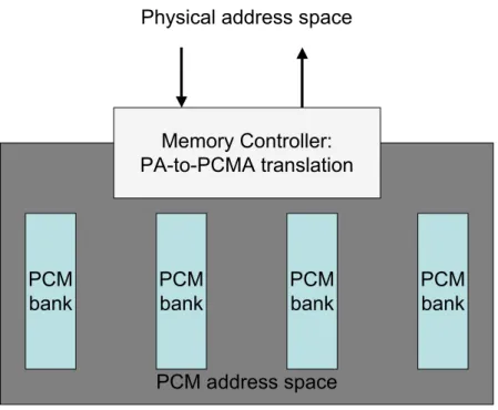
If a malicious attacker knows the PA-to-PCMA translation, then for a given PCM memory block B, he/she is able to figure out the address of the physical memory block that is mapped on B. If the PA-to-PCMA translation is made invisible from the outside of the PCM memory then the attacker can not retrieve the address of the physical
6 Andr´e Seznec
memory block mapped on a given memory block. Figure 1 illustrates this invisibility: the computer system manipulates data in the physical address space, but has no access to the PCM address.
Memory Controller:
PA-to-PCMA translation
PCM
bank
PCM
bank
PCM
bank
PCM
bank
PCM address space
Physical address space
Figure 1: Physical memory address space and PCM memory address space
3.1.2 PA-to-PCMA translations must dynamically change
Our analysis of the RBSG scheme has shown that, in order to resist a birthday paradox attack, the PA-to-PCMA translation of any physical block B has to be modified with a frequency largely higher than one time every W max possiblewrites on B.
The PA-to-PCMA translation changes should be completely unpredictable from the outside of the PCM mem-ory; in particular there should be no restrictions on the new translation. Through limiting the translation change possibility to a single region, the RBSG scheme is providing an overwrite attack possibility.
3.2
Principles of a practical secure PCM-based main memory
3.2.1 PA-to-PCMA translation
In the secure based main memory we propose, the PA-to-PCMA translation is performed by the PCM-memory controller through the use of a translation table. For a physical PCM-memory block B, the address of the corresponding PCM block is computed from an entry read in the translation table and the address B. The PA-to-PCMA translation must perform a one-to-one address translation from the physical address space to PCM address space.
The simplest mapping would be to associate a translation table entry with each physical memory block and en-suring that the translation is a one-to-one block mapping. Such one-to-one block mapping appears as unpractical: for instance 256M entries would be needed to map a 16 GBytes memory using 64 bytes memory blocks, leading to an indirect translation table requiring approximately a gigabyte of storage in the PCM memory controller to implement the translation table. Instead, we associate a single translation table entry with a region of R contigu-ous memory blocks; for instance if 4K contigucontigu-ous memory blocks are mapped by a single entry, 64K entries are sufficient to map 16 GBytes.
Towards Phase Change Memory as a Secure Main Memory 7
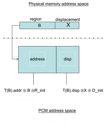
PA-to-PCMA region address translation Initializing at boot time the translation table T with a one-to-one region mapping is unpractical. Instead of such an initialization, we assume that at initialization time, the translation table T is initialized with only zeros, but that some computation is performed at run-time in addition to the read of the translation table. If memory regions are numbered from 0 to N-1, the translation is performed as follows: region B in physical memory is mapped onto region (T(B).address xor B xor R init), where R init is a random number generated at initialization time.
PA-to-PCMA region displacement translation The use of a single entry to map a complete region of the physical memory could lead to a possible overwrite attack on trying to write a specific block in all the regions, for instance the first block. In order to avoid such an attack, the displacement in the region is also translated. Physical memory block X in region B is mapped onto block ( T(B).disp xor X xor D init ) in region (T(B).address xor B xor D init). As R init, D init is a random number generated at initialization time. This PA-to-PCMA translation is illustrated on Figure 2.
T(B).addr ⊕ B ⊕R_init T(B).disp ⊕X ⊕ D_init B
region displacement
X
address disp
PCM address space Physical memory address space
Figure 2: PA-to-PCMA translation
More complex translation functions replacingD init and R init by functions randomly parameterized at ini-tialization time can be considered.
3.2.2 Dynamically changing PA-to-PCMA translation
In order to avoid blind overwrite attacks, the PA-to-PCMA translation must be continuously modified. More pre-cisely, only writes represent an issue. Therefore, the PA-to-PCMA translation modification is triggered randomly and only on memory writes.
This random triggering is particularly important: As an example, if the PA-to-PCMA translation change oc-curs periodically on writes, for instance every 10 writes, an attacker could repeat the sequence of nine consecutive writes on physical block B, one write on physical block C. Physical block C moves in the PCM memory, but block B remains on the same PCM memory location that can be easily overwritten.
8 Andr´e Seznec
How to modify PA-to-PCMA translation Modifying the PA-to-PCMA translation for a physical region B is implementing through swapping the translations for two physical regions. This guarantees that the PA-to-PCMA translation remains a one-to-one mapping. The region swapping induces the modification of two entries in the translation table as described below.
A random physical region B’ is chosen and the PA-to-PCMA translations of B and B’ are exchanged, i.e., T(B).address := old(T(B’).address) xor B’ xor B and T(B’).address := old(T(B).address) xor B’ xor B. At the same time, displacement translations inside blocks B and B’ are also modified,: T(B).disp: =old(T(B)).disp xor RAND and T(B’).disp: =old(T(B’)).disp xor RAND where RAND is randomly selected1.
The two memory regions in the PCM memory have to read and swapped accordingly.
Frequency of PA-to-PCMA translation modifications The cost of a PA-to-PCMA translation modification is proportional to the size R of a region in the memory. The two swapped regions have to be read and rewritten, i.e., a PA-to-PCMA translation modification induces 2 R memory block reads and 2 R memory block writes.
Therefore, the frequency of the address translation modification should be chosen in order to maintain the total overhead to a reasonable level. In this study, we arbitrarily estimate that inducing in average one extra write on the PCM memory per 8 effective writes would be acceptable. That is, in average one out of 16 R physical memory block writes can trigger a PA-to-PCMA address translation modification. Therefore on receiving a write on a physical memory block, the modification of its PA-to-PCMA translation is randomly triggered with probability
1 16R.
3.3
Putting all together in the memory controller
The design of a secure PCM-based main memory lead to several constraints inside the memory controller. 3.3.1 Write endurance and region size
The principles above in Section 3.2 lead to the design of a PCM-based main memory on which an overwrite attack would only be able to consecutively write the same memory block in average 16R times before the physical block is moved in another PCM memory block. In practice, a write attack could succeed in significantly reducing the lifetime of the memory, if 16R is not small with respect to the write endurance of the cells.
We run simulations of an overwrite attack on a 16 GBytes PCM memory i.e., 228 64-byte blocks. Regions of respectively 64K, 4K and 256 memory blocks were considered. If the memory features a write endurance of Wmax= 2Ewrites, then the theoretical write endurance of a uniformly accessed PCM memory is 228+E.
With a write endurance of only 8 Megawrites (223) per cell, using 64K memory blocks per region is not an
option: some memory blocks would be destroyed by a brute force overwrite attack in less than a billion (230)
writes. With 4K memory blocks regions, the PCM memory would be able to support an attack consisting of up to 38 % of the theoretical 251writes. With 256 memory block regions, this ratio would increase up to 71 %.
If the write endurance is 128 Megawrites per cell (227) then these respective ratios become 38 % for 64K memory blocks regions, 74 % for 4K memory blocks region and 85 % for 256 memory blocks region for a theoretical maximum of 88.88 % since in average one extra block write is triggered for 8 physical memory writes. If the write endurance is 1 Gigawrites per cell (230) then these ratios become 65 % , 83 % and 86% for 64K, 4K and 256 memory block regions respectively.
Therefore, if the technology is able to ensure write endurance in the billion range then even very large regions could be considered for PA-to-PCM translations.
3.3.2 Memory controller constraints
The secure PCM main memory would need to integrate extra hardware in the memory controller to implement the secure PA-to-PCMA translation.
Memory storage volume The storage volume of the PCM memory controller is a major issue. The main component is the translation table that features an entry per memory region. For a 16 GB memory, the use of regions of 256 64-bytes blocks would lead to 1 M entries, each entry featuring the address of region (20 bits) and a displacement in the region (8 bits) i.e. a total of 28 bits. The total storage cost of the translation table would be
1The same RAND is used since it allows to exchange the blocks one per one among the B and B’ regions.
Towards Phase Change Memory as a Secure Main Memory 9
3.5 Megabytes. Using larger granularity regions for instance 4K 64-byte blocks would lead to a much smaller 224 Kbytes translation table.
For a 256 GB memory, using 4K 64-bytes blocks regions would still appear possible since it would lead to a 4 Megabytes translation table. For such a 256 GB memory and 64K 64-byte blocks regions would only necessitate 256 Kbytes for the translation table.
Swapping memory regions logic The memory controller has to handle the important function of swapping two memory regions on a PA-to-PCMA translation change. This induces a large number of memory reads and writes. An atomic swap of the two memory regions would stop the normal read and write accesses by the computer system . This would not unacceptable.
Therefore the memory controller must feature logic to interleave blocks swapping with the normal flow of reads and writes from the computer system. The logic must be able to handle the case where a normal write is overwriting a block belonging to one of the memory regions being swapped. Moreover this normal flow of writes may randomly trigger new region swaps; the memory controller should be able to buffer these swaps.
The priority on writes must be dynamically adapted in order to maintain a limited number of regions waiting for swaps, for example at most 8 swaps. As an example, we tested a policy randomly splitting the write priority to 1/4th for region swapping and 3/4th for normal write flow when less than 4 region swaps are waiting and one half for region swapping and one half for normal write flow when 4 or more region swaps. On an experiment on 240writes and assuming a continuous saturated write flow from the computer system, there was never more then
8 waiting region swaps.
Extra PA-to-PCMA translation latency The extra access time to main memory due to PA-to-PCMA translation is essentially due to the read of the PA-to-PCMA translation table. This table will be implemented as a SRAM table in the memory controller. For a 16 GB memory using 4K 64-byte blocks region, the read access time of a 224Kbytes SRAM memory would in the range of 3-5 processor cycles and would be marginal compared with the overall main memory access time.
The random number generator Our secure PCM-based main memory will be able to resist to an overwrite attack if no one is able to follow or reconstruct the PA-to-PCMA translation process. Our proposal heavily relies on a random number generator. The security of our proposal also depends of the security of this random number generator.
One can remark that the output of the random number generation used in our memory controller cannot be di-rectly observed from the outside of the PCM memory. Therefore different possible schemes could be implemented ranging from a true hardware random generator to a simpler algorithmic pseudo-random number generator per-sonalized with a huge key at manufacturing time.
3.4
A secure PCM main memory might become practical in a few years
A need for large write endurance per cell A rule of thumb that has been approximately respected for the past 10 years has been that in general purpose computer systems, the processor was able to write its complete main memory in a second. That is if a system features X GBytes, its achievable memory write bandwidth is in the X GBytes/s range.
This rule of thumb is very useful to determine at which write endurance threshold, the PCM technology will become reliable enough to consider using it as main memory for computer systems. As Qureshi et al [2], we approximate a year by 225seconds. Therefore, a memory system randomly and uniformly exercised at full write bandwidth will necessitate a endurance per cell of 225writes per cell and per year of expected life of the system.
That is a write endurance per cell of 256 Megawrites for 8 years and 1 Gigawrites for 32 years.
Economic feasibility of PCM main memory If within a few years, the write endurance per cell on PCM components reach a billion writes then it would become feasible to build 16 GBytes (or larger) memory using comparatively very small PA-to-PCMA translation table (for instance, using 64K memory regions): as mentioned above, the secure PCM memory would be able to survive to an overwrite attack at full write bandwidth for 65 % of an expected lifetime of 32 years.
10 Andr´e Seznec
Page mode is compatible with security If PCM memories are used as main memory then a page mode would be interesting as on current DRAM to limit the access latency and increase bandwidth when the memory read requests exhibit high spatial locality. Our PA-to-PCMA translation scheme is compatible with such page mode since regions are large enough to accommodate large page, even split across several PCM components.
4
Conclusion
If the promises of the PCM technology are fulfilled (4X higher integration density, 1 billion write endurance per cell, access time in the same range as DRAMs, dynamic energy consumption in the same range as DRAMs) then it will become economically feasible to build a main memory from PCM memory component in the next few years. Such a PCM-based main memory will particularly be attractive due to its very low static energy consumption. However to consider such a memory for an industry product , the PCM based memory would have to be able to resist to software overwrite attacks targeting its physical destruction.
In this paper, we have proposed a first secure PCM based main memory that will resist to overwrite attacks . By hiding the effective PCM memory address from the rest of the computer system and continuously and randomly moving the physical memory blocks in PCM memory, overwrite attacks are made impossible. The proposed PA-to-PCMA translation scheme uniformizes and randomizes the write flow on PCM memory for malicious overwrite attacks as well as conventional non malicious applications. Our scheme requires some hardware overhead in the memory controller (essentially a PA-to-PCMA translation table, the memory region swapping logic and a random number generator). But it brings the practical write endurance of the overall PCM main memory in 70-85 % of the theoretical write endurance of a uniformly accessed PCM memory.
5
Acknowledgments
This work was partially supported by the European Commission in the context of the SARC integrated project #27648 (FP6).
References
[1] B. C. Lee, E. Ipek, O. Mutlu, and D. Burger. Architecting phase change memory as a scalable dram alternative. In ISCA, pages 2–13, 2009.
[2] M. K. Qureshi, J. Karidis, V. Srinivasan, M. Franceschini, L. Lastras, and B. Abali. Enhancing lifetime and security of pcm-based main memory with start-gap wear leveling. In Micro, dec 2009.
[3] M. K. Qureshi, V. Srinivasan, and J. A. Rivers. Scalable high performance main memory system using phase-change memory technology. In ISCA, pages 24–33, 2009.
[4] S. Raoux, G. W. Burr, M. J. Breitwisch, C. T. Rettner, Y.-C. Chen, R. M. Shelby, M. Salinga, D. Krebs, S.-H. Chen, H.-L. Lung, and C. H. Lam. Phase-change random access memory: a scalable technology. IBM J. Res. Dev., 52(4):465–479, 2008.
[5] P. Zhou, B. Zhao, J. Yang, and Y. Zhang. A durable and energy efficient main memory using phase change memory technology. In ISCA, pages 14–23, 2009.
Centre de recherche INRIA Rennes – Bretagne Atlantique IRISA, Campus universitaire de Beaulieu - 35042 Rennes Cedex (France)
Centre de recherche INRIA Bordeaux – Sud Ouest : Domaine Universitaire - 351, cours de la Libération - 33405 Talence Cedex Centre de recherche INRIA Grenoble – Rhône-Alpes : 655, avenue de l’Europe - 38334 Montbonnot Saint-Ismier Centre de recherche INRIA Lille – Nord Europe : Parc Scientifique de la Haute Borne - 40, avenue Halley - 59650 Villeneuve d’Ascq
Centre de recherche INRIA Nancy – Grand Est : LORIA, Technopôle de Nancy-Brabois - Campus scientifique 615, rue du Jardin Botanique - BP 101 - 54602 Villers-lès-Nancy Cedex
Centre de recherche INRIA Paris – Rocquencourt : Domaine de Voluceau - Rocquencourt - BP 105 - 78153 Le Chesnay Cedex Centre de recherche INRIA Saclay – Île-de-France : Parc Orsay Université - ZAC des Vignes : 4, rue Jacques Monod - 91893 Orsay Cedex
Centre de recherche INRIA Sophia Antipolis – Méditerranée : 2004, route des Lucioles - BP 93 - 06902 Sophia Antipolis Cedex
Éditeur
INRIA - Domaine de Voluceau - Rocquencourt, BP 105 - 78153 Le Chesnay Cedex (France)
http://www.inria.fr