OATAO is an open access repository that collects the work of Toulouse
researchers and makes it freely available over the web where possible
Any correspondence concerning this service should be sent
This is an author’s version published in:
https://oatao.univ-toulouse.fr/18131
To cite this version:
Favre, Philippe and Reynes, Jean-Michel and Favre, Jacques Real
3D-packaging: a breakthrough for high power electronics for
automotive applications. (2015) Société des Ingénieurs de
l'Automobile - SIA. 1-8. ISSN 0368-2579
Real 3D-packaging: a breakthrough for high power electronics for
automotive applications.
Ph. Favre
1, J-M. Reynes
1, 2, J. Favre
11: aPSI3D, 67bis boulevard Pierre Renaudet, 65000 Tarbes, France
2: IRT Saint-Exupery, 31432 Toulouse, France
Abstract: Power electronics stands at the crossroad
of highly convoluted disciplines of physics: thermal science, mechanics and electronics. In order to respond to the growing and demanding automotive market, designers have no choice but to assemble off-the-shelf parts, keeping the onus of managing themselves thermal losses and stray inductances at interfaces. Power mechatronics is the buzz word for this. It has for long envisioned double-sided cooling and wire-bondless interconnections as ways to go. Merging those impediments and opportunities into a global solution, aPSI3D has developed an integrated
approach for multi-physical co-design with its customers, offering both plug-in cooled power modules and maximum value transfer to the inverter. Eventually, a 50% power module with imbedded cold plate size reduction for a 100kW inverter is obtained vs. state-of-the art pin fin standard products.
With a 10nH stray inductance, this solution is paving the way to more than 100A wide bandgap semiconductor die based highly efficient power modules.
Keywords: Power, module, low inductance,
double-sided cooling, three dimensional packaging, power mechatronics.
1. Introduction
The emergence of power electronics in the automotive industry is a direct consequence of electrification and hybridization, but will this happen? All car manufacturers are dreaming to avoid such solutions, too complex and expensive, by optimizing the performance of their thermic engines, can they succeed?
A genuine 3D-packaging solution is coming, closing the feasibility gap of complexity, cost efficiency and compactness. We shall review the technical criteria that should drive to success.
2. The upcoming regulatory constraints
2.1 Trend to Hybridization
The potential massive arrival of hybridization is no longer a matter of fuel price but becomes a consequence of regulation.
The petrol price remains a potential accelerator, in case the barrel passes 150$, but now at 60$/barrel,
the consumer is just not considering fuel economies as a driver to choose its new car. In the USA, 50% of the owners of a Hybrid car will not renew that choice, not because they are unsatisfied by the product but just because they do not consider it as a necessity of the moment. So the main three drivers will be Tax, emissions regulation and local rules:
• In countries where the CO2 tax is heavy (In France for 151g you pay 1600€, for 180g 3000€ once as private customer and 3200€ per year as a company), the trend to look for efficient cars in fuel economy is very strong but so far diesel is able to answer to this expectation.
• But from 2019-20 and even more from 2025, the very strict targets for fuel efficiency will result in a share of hybridization, when or if the thermal engine comes at the end of its improvement.
• In addition, hybridization and electrification are the only solutions to enter in cities planning to ban all cars but zero emissions.
2.2 Trend to electrification
The first steps of electrification are shy but the real success of car sharing (like Autolib) and the good performance of EVs on the market have convinced the end-customer that fun-to-drive would not die with electrical driving.
There remains a huge improvement margin on batteries in terms of cost and power density that would lead to a more competitive offer compared to thermic engines. The solutions to charge in one or two minutes already exist but the installed infrastructure and electrical network will not allow it. Then EV can be a clean solution, but not always, depending on the way electricity is produced.
Figure 1: The actual emission of EV from well to wheel
2.3 The Empty Basket of emission reduction solutions
The improvement of emissions of gasoline engines on the market has been led by, gasoline direct injection coupled with turbo, variable valve timing, variable valve actuation, exhaust gas recirculation (more on diesel), start stop and for some OEMs lean-burn, still offering some potential, etc.
The last major improvement will result from the introduction of variable compression engines. Audi announced a launch in 2017, others will follow. But it is likely the last major breakthrough on emissions and performance improvement with a potential of 6 to 12%. All other known ideas stay in the range of 1%.
In 2020, small 3 cylinder 1 Litre GDI engines will pass with asthenic performances but the bigger size fitted in vehicles above1.2 tons will have to move to variable compression or hybridization, maybe both on the longer term.
Therefore we can be sure that hybridization will take off, strongly between 2020 and 2030. Electrification will have a place, between 5 and 10%, for sure no more before 2030.
3. The small and light inverter
3.1 The car-body, an almost full basket
How can we imagine, when opening the hood of a vehicle, to introduce an additional electric motor maybe with a speed reducer, some batteries and an electronic inverter. No room and more weight is our constraint.
3.2 The technical keys for success
aPSI3D is contributing to the next generation inverter
by responding to the following expectations:
• Dissipate calories in a small volume.
• Dissipate calories in a hot environment but offer a high reliability.
• Work fast: high frequency is necessary to monitor fast electrical engines, to be used to optimize weight and size.
• Design robustness for high volume production.
SMALL, FAST-SWITCHING, ROBUST, HEAT-SINKING, are our technical key words for success. Eventually, in order to comply with the necessary compactness, the ideal inverter is to demonstrate optimal Integration balance between
• DC bias
• Self-Inductance
• Thermal management
• Interface control (design robustness)
4. DC bias
4.1 Power switching elements
By increasing their die size, silicon power devices can support large current, whatever their DC voltage capability, from few tenths up to hundreds of volts. Along with the development of microelectronics wafer manufacturing of large integrated circuits, such power devices can now be efficiently produced in volume. As a matter of fact the current is now the limiting factor at the system level, because of the cost and weight of the copper required to handle high currents. One way to reduce the amount of conducting material is to increase the DC bias voltage, e.g. via the batteries.
4.2 Overvoltage
In the same time, the power device technologies have been improved to deliver low ON resistance and extremely low switching losses. Thanks to the combined localized emitter efficiency and localized lifetime recombination controls, and to the minority carrier control at the cathode side via trenches or via the CSTBT concept. [1; 5]
However the amount of time required for switching off the power devices is so low that it induces extremely high di/dt which in turn generates overvoltage all along the commutation loop through parasitic self-inductances. This is a very well-known mechanism. In section number 5, we shall describe with some details how 3D packaging optimizes those self-inductances.
4.3 Actual trends in manufacturing
By carefully controlling the amount of minority carriers injected through the back diode of an IGBT or through the regular front side of a power diode, at any time, at any location, mainly vertically, including outside the active area of the power devices, more robust devices were made available for higher frequencies, up to 20 kHertz, at high current (typically >100 A)..
However changing the material and removing the minority carriers from the equation is offering one way to exceed this frequency limitation. Wide bandgap semiconductors, and more precisely SiC Schottky diodes and unipolar SiC Mosfet and unipolar GaN transistors are paving the way to replace silicon diodes and IGBT.
These new materials are not fully mature yet; they exhibit some manufacturing yield limitation which in turn are limiting their die size and current capabilities. Consequently it is mandatory to parallel these power devices to get the desired nominal current for a given application.
Paralleling such devices at the expense of multiple wire bonding operation restrains their frequency capability. Real-3D-Packaging provides an elegant solution to that limitation. As power need rises, the di/dt will most likely increase, so that the “geometrical” parasitic self-inductances will require more attention to be paid.
5. Self-Inductance
5.1 Self-Inductance estimation
As depicted in [6], building power modules can become extremely expensive and time consuming, especially if we want to experience low self-inductances. In order to properly design the power module before fabrication we have drawn multiple modules using solid-edge software and imported them into Q3D Extractor from Ansoft. Then, material properties and boundary conditions have been defined properly. Considering nowadays silicon die switching capabilities, we have selected the AC calculation which is good enough for illustrating the di/dt through the commutation loop (>5 Mhertz). 5.2 Copper balls versus pads on front metal electrodes
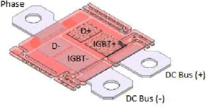
The inner part of the power module is partially drawn in Figure 2, where heat sinks, plastic package, gate and sense electrodes were removed to better show the electrical connections of interest:
• AMB to DC bus electrodes.
• AMB to Phase electrode.
• Copper balls joining the High Side power dies to the AMB (Phase electrode).
• Copper balls joining the Low Side power dies to the AMB (DC bus (-) electrode).
Figure 2: Power module main electrodes
All elements were disposed onto the AMB layers, as much as possible in a symmetrical way. However the gate electrodes and sensing elements are modifying slightly the AMB routings. We have extracted the parasitic inductance through the conventional
commutation loops with one IGBT from one side and one diode from the opposite side and vice versa. One extra simulation considers all power dies conducting together the current (this is a fictitious hypothesis, as dies are considered as resistors in such a modelling software, for the sake of
highlighting the contribution of the current path length). The simulations were conducted with source and sink excitation through the edges of the holes made in the bus connectors, or through the AMB edge layers with the bus connectors removed. In parallel we have conducted other simulations by replacing the copper balls by copper pads instead (not drawn here).
Exitation Dies ON Copper balls (nH) Copper pads (nH) % offset
Connectors All 9,55 9,4 1,57
Connectors IGBT+ D- 10,33 10,04 2,81 Connectors D+ IGBT- 10,4 10,15 2,40
AMB edges All 5,84 5,6 4,11
AMB edges IGBT+ D- 6,67 6,6 1,05 AMB edges D+ IGBT- 6,85 6,54 4,53
Table 1: self-inductance estimation using copper balls versus copper pads.
From table 1 we can make several comments:
• Similar results whatever the commutation loop, which means we have a good balance (symmetry) between both sides.
• Similar results whatever the number of components conducting the current.
• Quite strong impact from the power bus connectors (40% of the total value).
• Quite small offset between copper balls versus copper pads, in the same range of the Q3D desired precision.
However due to the large number of copper balls that we use to reduce the current density through each copper ball, each simulation lasts 3 hours, at least, for such a simple case with a limited amount of devices. Using copper pads instead, which are disposed onto the silicon pads, the simulation is performed in 2 minutes - instead of 3 hours - which is a very significant drop in time. At least we are sure that the system is converging. Results show a minimal offset of less than 4%. This was expected due to the proximity of the copper balls which pushes away the magnetic field distribution outside the silicon pad location. Thus, for the next Q3D computations shown in this publication, we have replaced the copper balls by the copper pads.
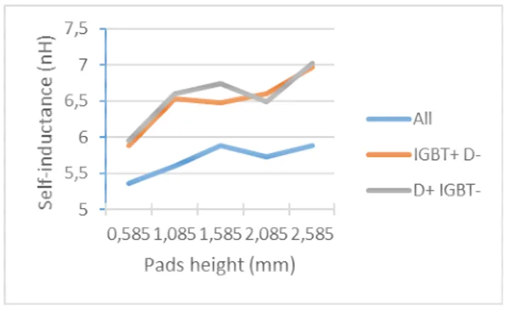
5.3 Copper pad thickness impact
As can be seen from the last table, it is almost impossible to figure out how much the copper ball is
inducing in term of parasitic inductance, even in the case where the power bus connectors are removed. So we just made extra simulations with the copper pad height as the main variable as depicted below, in Figure 3.
Figure 3: self-inductance variation with pad height Considering the copper pad self-inductance amount in the case of 2 power dies within the commutation loop, we can estimate the copper pad parasitic inductance to be in the range of 0.1nH per die with a pad height of 0.585 mm. This result is consistent with the case where all dies are conducting with twice more copper pads in parallel.
For applications requiring higher voltages, the copper pad will have to be increased accordingly. This will increase the self-inductance which will stay however far below the one coming from the use of long wires instead. (10X reduction at least).
5.4 Double power module impact
We have studied another application requiring more power by doubling the number of dies, either diodes and IGBT, using the same concept previously described.
Figure 4: “double” Power module main electrodes In order to extract the self-inductance we have considered multiple combinations of one device per side with another device at the opposite side just to
figure out what would be the location impact, if any, and what would be the resulting variability we could expect from such large power module. The closest die to the DC bus is named “1”, while the closest die to the Phase connector is called “4”.
die position side - / side + 1 2 3 4 1 9,2 9,64 10,43 10,7 2 9,34 10,44 11,41 10,59 3 9,77 10,26 10,74 14,38 4 10,34 10,75 11,39 12
Table 2: self-inductance variation with die combination between upper and lower sides.
From table 2 we can make several comments:
• Similar results as compared to case 1 using twice less dies, in the range of 10 nH.
• The closer the commutation loop to DC Bus, the smaller the self-inductance value.
• The closer the commutation loop to Phase, the larger the self-Inductance value.
• There is still a symmetry in the results. However the commutation loop path was increased by a factor 2 compared to case 1, and we do not observe a factor 2 increase for the self-inductance. This is consistent with the power connectors which represent a large amount of the total self-inductance, and consistent with the mutual inductance resulting from the proximity of Phase to DC electrodes through the entire AMB layers. Both AMB layers are face-to-face and we have been very cautious when drawing the routings facing one another. This mutual inductance phenomenon is very well known and described in the literature [7; 10].
To illustrate its impact, we have extracted self-inductances between the DC bus and the Phase, by providing 2 sources (power connectors) and one sink (at the Phase connector). The coupling number between the 2 sources was provided by Q3D. As expected the sum of the self-inductances per side minus twice the coupling number is giving us the self-inductance already extracted between the DC bus, with a small offset (< few %).
5.5 Copper balls current density through parallel diodes
Q3D software is giving us a figure of merit relative to the self-inductance which is mainly linked to the “geometrical” aspect of the power module, whatever the current density going through the power dies. However there is one specific case where putting bipolar diodes in parallel may induce large current imbalance and produce thermal instabilities due to their negative temperature de-rating coefficient. For that particular case we have used the same solid-edge software and have imported the modules into the Maxwell Extractor from Ansoft. All simulations
were performed in DC mode and a continuous current of 300 Amperes was applied between the DC bus and the Phase electrode, through both diodes from the same side conducting in parallel.
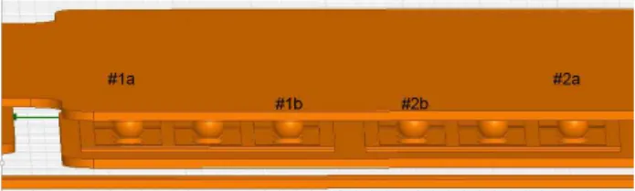
To illustrate our findings, we have defined few rectangles (not represented here) within Maxwell software to quantify the current that flows through selected copper balls on top of the 2 High Side diodes as depicted in Figure 5, which is almost a cross section of Figure 4.
Figure 5: High Side diodes and 6 rectangles positioned in the middle of selected copper balls to extract the current density. (not-drawn).
Copper ball #1a diode 1 is closer to the Phase. Copper ball #1b diode 1 is farther from the Phase. Copper ball #2a diode 2 is closer to the DC bus. Copper ball #2b diode 2 is farther from the DC bus.
Silicon Resistivity
Current Copper Tantalum 300 S/m
#1 127 143 150 #2 180 156 149 #1a 25 9.7 8.9 #1b 1.2 7.2 7.9 #2a 25.9 10.1 8.9 #2b 3.1 7.7 8
Table 3: Current per diode (first 2 lines) and current density per copper ball per diode (last 4 lines) versus silicon resistivity.
As can be seen from Table 3, the silicon resistivity was chosen to comply with the VForward voltage of the diodes at the nominal current of 300 Amperes, which correspond to 300 Siemens per meter. Using copper material instead, with a resistivity of 60 Millions of Siemens per meter may induce wrong indications of the current density through each diode put in parallel. (127 Amperes vs. 180 Amperes!).
6. Thermal Management
6.1 Usual approach
Standard modules are evidencing a mismatch: although dies are the highest cost contributor, they are underutilized. Typically, an area corresponding to 800A are used for a nominal 500A max rating.
People could argue that this is just targeting a reduction of Ron, but this is actually limited by the ability to drain heat away.
Indeed, heat sinking is the first limitation to compactness. How to alleviate it?
For a given switching frequency, swapping silicon with SiC or GaN should save energy. This is one face of the equation.
Another face of it consists in reducing thermal resistance (Rth). Spreading heat on a wider surface is irrelevant for automotive powertrain, which requires size reduction. Thermal resistance per unit area is the one parameter to trim down.
Improving intrinsic material conductivity and interface quality is a valid way for all options. How to design an acceptable trade-off with cost is a conundrum; though.
6.2 Double-sided cooling pros and cons
Double-sided cooling is an easy concept. It creates a highly conductive parallel path through the front side of the dies, which reduces Rth without expanding the used area. [11].
How much can we expect to reduce the thermal resistivity? A rough and easy estimate yields an additional 70% heat flow, proportional to the typical front side bottleneck (the pad area) vs. the die area. That means that such a device would drain 40% of its calories through the front side, and 60% through the back side.
How much does an actual device yield? [12] Thermal modelling claims a ratio 25%/75%, that rigorous characterisation will confirm soon.
Double-sided devices have been worked on for years, with little, if any, industrial outcome, despite many announcements and publications. What are the reason for this?
At low voltage, the cost constraint and heat amount have most likely been the show stoppers.
At higher voltages (> 300V), the main two hindrances are voltage sustaining, as conductors are facing one another in a narrow, hardly controllable space, and processability.
Direct bonding is the ideal version where the die front side pads are directly bonded onto the top substrate. [13] Unfortunately, the tiny distances between both substrates makes it difficult to guarantee voltage sustaining along the device. Moreover:
• Having multiple polarizations on the front side of dies makes the process trickier: design rules at the substrate level have a poorer pitch than the dies.
• Targeting multiple dies on a same module, possibly with different die thicknesses, and for sure with a substrate larger area, makes it difficult to guarantee actual and uniform bonding of each pad.
Figure 6: Direct (double-sided) bonding is limited in voltage.
All kinds of spacers, e.g. clips, cylinders, balls, were considered. Copper double step etching is a possible solution, with the limitation of etching pitch compatibility [14]. The solution that was proven [15] the most appropriate with regard to thermo-mechanical robustness is bumping.
Figure 7: voltage sustaining demands a spacer insertion.
The larger the component, the worst the ability to process. Any product D-FMEA points out how critical thermal and electrical resistances of such spacers must be controlled. A smart process integration is the mandatory key to enable and guarantee the benefits to the product of such a double-sided component.
6.3 Cooling close dies
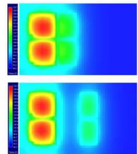
Depending on the actual cooling, efficiency, thermal coupling between dies becomes dominant. Improving heat sinking permits the dies to be closer. Regular datasheet are confusing as they report low power thermal resistance, which totally neglects thermal coupling between dies. This is an additional variability the user must deal with, which depends on the variability of the thermal interfaces from dies to coolant.
Figure 8 shows a simulation of two IGBTs and two diodes in a fully integrated double-sided cooling configuration [16]. Comparison of typically 1 mm and 1 cm spacing shows a 1 degree elevation only of IGBT temperature from 131.4°C to 132.4°C, when running rather high current.
With such a cooling configuration, module compactness can be significantly improved.
:
Figure 8: Two IGBTs and two diodes in a double-sided cooling configuration. Comparison of 1mm and 1cm spacing [16].
6.4 Heat sink vs. pressure drop
Independent of the double-sided structure, heat sinks are a key contributor to thermal performance. The whole challenge consists in having the shortest thermal path from dies to coolant, with minimal interface losses.
Many geometries can be considered. Figure 9 shows a set of data with regular fin heat sink, the pitch and fin thickness of which were varied. Here, a lower limit was forced by a minimum value of the pitch, related to the particulate sizes in the coolant, in order to avoid clogging.
.
Then, the fluid repartition across the heatsink is instrumental.
Figure 9: IGBT temperature vs. pressure drop at maximum current. Dots correspond to different fin
thicknesses and spacing of fins in a double-sided cooling power module [16].
7. Interface control (design robustness)
7.1 Global integration
Power electronics integration is complex, mostly
because of incompatibilities between materials and
processes, which can be understood as due to
coupling of multiple disciplines of physics. The
limiting criteria of device performance are a
convolution of the ability to drain heat away, to keep
self-inductances low and to master the mapping –
and surges – of electric fields. Each of those criteria
has a direct impact on device aging [17, 18].
Currently, building blocks for power electronics are
designed and acquired separately. They are
assembled within an often imperfect frame of
utilization rules.
Thus, there is an uncharted area for combined
optimization of such hardly controlled interfaces. All
coupling, should be managed at the design stage of
power modules. This requires a cross-fertilization of
the disciplines of physics such as thermal
management, fluidics, mechanics, electrokinetics,
electronics, electromagnetism and physics of solids.
Thanks to a simultaneous optimisation of that whole
set of input parameters, while understanding the
actual correlation causes, there is no more need to
add up safety guard bands to cover those interface
uncertainties ; conversely, it has become possible to
control and significantly reduce the global
variability. Global mastery induces new permitted
topologies, which makes it possible for technologies,
unconsidered until recently mostly because of the
traditional interface management approach, to show
up.
With such an integrated design process, we give a
real meaning to the concept of Power Mechatronics.
7.2 Process control
Contrary to the usual approach that consists in
assembling objects that did not go through a
common design process, we promote a global design
so that all variabilities are considered upfront all
together, for a global optimisation. Therefore, users
must get prepared for a paradigm shift. What they
have considered as inevitable dispersion of
performance, for years, and all kinds of historical
rules of thumbs inherited from experience must be
revisited.
Below is a schematic of what a double-sided power
module looks like. Each process step necessary to its
fabrication must abide to similar process controls, so
that each physical property obeys to similar spread.
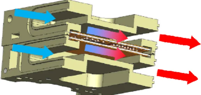
Figure 10: A double-sided cooling integrated power module. Coolant is heated from left to right, while flowing along both substrates.
From section 5, we demonstrated that parasitic
inductances are actually showing very little
variation. Similarly, as neither thermal grease, nor
thermal interface material is necessary, interface Rth
is reduced to the heat think joining process spread
itself, and the interactions with the rest of the
fabrication process.
Eventually, the key factor of success stands in the
process integration that we shall not detail here, as it
is being patented.
8. Conclusion
The good news is that the necessary effort of
innovation is resulting in a truly mechatronic
solution which, thanks to a simplified bill of
material, wire bond removal and a proper process
integration anticipated at the global design phase, is
getting
a
lead
in
reliability,
performance,
compactness
and
cost
competitiveness. That
differentiation was made possible by a utilization
paradigm shift that the market still needs to accept.
Thus, we are ready to welcome the expected fast
ramp-up of power mechatronics in automotive. The
innovation flow should follow with wide bandgap
semiconductors, the switching speed of which will
demand lower inductances such as those offered by
3D-packaging, only.
9. Acknowledgement
This work was first made possible by more than 10 years of experience accumulated in Primes Innovation Platform in Tarbes. In depth
characterisation was helped by ENIT and IRT Saint-Exupery. At last, industrialization has been supported by CEA Tech.
10. References
[1] T. Laska: "A 2000V Non Punch Through IGBT with dynamical properties like a 1000V IGBT”, IEDM, San Francisco, CA, USA, 1990.
[2] H. Brunner: "Progress in development of the 3.5kV high voltage IGBT / Diode chipset and 1200A module applications", IEDM, Washington, DC, USA, 1997.
[3] M. Kitagawa: "A 4500V Injection Enhanced Insulated Gate Bipolar Transistor (IEGT) Operating in a mode similar to a Thyristor", IEDM, Washington, DC, USA, 1993.
[4] H. Takahashi: "Carrier Stored Trench-Gate Bipolar Transistor (CSTBT) A novel power device for high voltage application”, ISPSD, Maui, Hawaii, USA, 1996.
[5] A. Mauder: "Vertical power semiconductor component”, Patent US2005/0035405A1, 2005. [6] Shengnan Li: "Packaging Design of IGBT Power
Module Using Novel Switching Cells", Doctoral Dissertations, University of Tennessee, Knoxville, USA, 2011.
[7] JM. Guichon: "Busbar Design: How to Spare Nanohenries", Flux magazine N°53 January 2007. [8] Dr. R. Bayerer: "Power Circuit design for clean
switching", CIPS2010, March, 16-18, Nuremberg, Germany, 2010.
[9] G. Borghoff: "Implementation of low inductive strip line concept for symmetric switching in a new high power module”, PCIM Europe 2013, 14-16 May, Nuremberg, Germany, 2013.
[10] S.S. Wen: "Design and Thermo-mechanical Analysis of a Dimple-Array Interconnect Technique for Power Semiconductor Devices”, Ph.D. dissertation, Virginia Polytechnic Institute, USA 2002.
[11] Dr M. Schneider-Ramelow: "Design and assembly Thermo-mechanical Analysis of a Dimple-Array Interconnect Technique for Power Semiconductor Devices”, CIPS, Singapore, 2008.
[12] M.H. Poech: "Advantages of double-sided cooling
concepts for Power Semiconductors”,
https://www.powerguru.org/wordpress/wp-content/plugins/ckeditor-for-wordpress/ckeditor/ Web posted on 14 June 2012.
[13] H-R Chang: "300A 650V 70 um Thin IGBTs with Double-Sided Cooling”, ISPSD 2011, San Diego, California, USA, 2011.
[14] R. Riva: “Solution d’Interconnexions pour la Haute Température”, Thesis 2014ISAL0064, INSA Lyon, France, 2014.
[15] A. Cissé: “Numerical modelling of a high temperature power module technology with SiC devices for high density power electronics”, PCIM Europe, Nuremberg, Germany, 2012.
[16] X. Chauffleur: “Thermal and fluidic design for automotive application”, IMAPS Thermal Management (La Rochelle, France) 2015
[17] M. Mermet-Guyennet: "New structure of power integrated module”, CIPS, Naples, Italy,2006. [18] P. Solomalala: “Virtual reliability assessment of
integrated power switches bases on multi-domain simulation approach”, Proceeding ESREF, Arcachon, France, 2007.
11. Glossary
CSTBT: Carrier Stored Trench Gate Bipolar Transistor Ron: On-state resistance of a transistor
Rth: Thermal resistance
D-FMEA: Design Failure mode and effect analysis. IGBT: Insulated Gate Bipolar Transistor.
SiC: Silicon Carbide GaN: Gallium Nitride.