O
pen
A
rchive
T
OULOUSE
A
rchive
O
uverte (
OATAO
)
OATAO is an open access repository that collects the work of Toulouse researchers and
makes it freely available over the web where possible.
This is an author-deposited version published in :
http://oatao.univ-toulouse.fr/
Eprints ID : 17905
To link to this article : DOI:10.1016/j.scriptamat.2017.05.008
URL :
http://dx.doi.org/10.1016/j.scriptamat.2017.05.008
To cite this version :
Mesguich, David and Arnaud, Claire and
Lecouturier, Florence and Ferreira, Nelson and Chevallier, Geoffroy
and Estournès, Claude and Weibel, Alicia and Josse, Claudie and
Laurent, Christophe High strength-high conductivity carbon
nanotube-copper wires with bimodal grain size distribution by spark
plasma sintering and wire-drawing. (2017) Scripta Materialia, vol.
137. pp. 78-82. ISSN 1359-6462
Any correspondence concerning this service should be sent to the repository
High strength-high conductivity carbon nanotube-copper wires with
bimodal grain size distribution by spark plasma sintering
and wire-drawing
David Mesguich
a, Claire Arnaud
a,b, Florence Lecouturier
b, Nelson Ferreira
b, Geoffroy Chevallier
a,c,
Claude Estournès
a,c, Alicia Weibel
a, Claudie Josse
a,d, Christophe Laurent
a,⁎
aUniversité de Toulouse, CIRIMAT, CNRS-INPT-UPS, Université Paul-Sabatier, 118 route de Narbonne, F-31062 Toulouse cedex 9, France bLaboratoire National des Champs Magnétiques Intenses, UPR3228 CNRS-UPS-INSA-UGA, 143 avenue de Rangueil, F-31400 Toulouse, France cPlateforme Nationale CNRS de Frittage Flash, PNF2, MHT, Université Paul-Sabatier, 118 route de Narbonne, F-31062 Toulouse cedex 9, France dUniversité de Toulouse, Centre de Microcaractérisation Raimond Castaing, UMS 3623, Espace Clément Ader, 3 rue Caroline Aigle, 31400 Toulouse, France
a b s t r a c t
Copper and 1 vol% carbon nanotube-copper cylinders with a micrometric copper grain size and either a unimodal or a bimodal grain size distribution were prepared using spark plasma sintering. The cylinders served as starting materials for room temperature wire-drawing, enabling the preparation of conducting wires with ultrafine grains. The tensile strength for the carbon nanotube-copper wires is higher than for the corresponding pure cop-per wires. We show that the bimodal grain size distribution favors strengthening while limiting the increase in electrical resistivity of the wires, both for pure copper and for the composites.
Keywords: Copper Carbon nanotubes Spark plasma sintering Wire-drawing Nanostructured materials
There is a demand for stronger conducting wires, in fields such as aeronautics, space, energy and high-field magnets. Established methods to strengthen metals, like cold working, alloying or introducing another phase, simultaneously decrease the electrical conductivity through the introduction of defects[1–4]. However, a specific type of grain bound-ary, the coherent twin boundbound-ary, was shown to strengthen electro-chemically-deposited copper films without introducing additional electron scattering[5]. Similar results were reported for nanotwinned bulk materials[6]and wires[7,8]prepared using cryo-deformation. We have reported[9]an innovative approach combining spark plasma sintering (SPS) and room-temperature (RT) wire-drawing to produce Cu wires with both a high ultimate tensile strength (UTS) and high elec-trical conductivity. The short sintering times used in SPS[10]permit to produce Cu cylinders (to be wire-drawn) with an ultra-fine microstruc-ture, ten times smaller than for conventional cylinders[9,11]. Strength-ening of the wires originates from the propagation of dislocations by an Orowan-type dislocation glide mechanism in grains smaller than 250 nm[9]. Double-walled carbon nanotube (DWCNT)-Cu wires show a higher UTS than the Cu wires but also a higher resistivity at 77 K
[12]. Here, we show that the preparation of SPS cylinders with a bimod-al, as opposed to unimodbimod-al, Cu grain size distribution ultimately favors
strengthening the wires while limiting the increase in electrical resistivity.
The CNT sample (Nanocyl, Belgium) was described elsewhere[13]. The number of walls and external diameters were measured for about 100 CNTs on HRTEM images. CNTs with 3–22 walls are observed but CNTs with 7–9 walls are dominant, representing 62% of the total. Exter-nal diameters are in the range 5.8–18.8 nm and the average exterExter-nal di-ameter is equal to 10.2 nm. Length is below 1.5 μm. The CNTs were carboxyl-functionalized with a nitric acid solution (100 °C, 3 mol·L− 1)
[14]. Commercial spherical Cu powders (Alfa Aesar, 99%) were used, with either a unimodal (d10,d50and d90= 0.45, 0.76 and 1.36 μm,
re-spectively) or a bimodal (d10,d50and d90= 0.63, 1.33 and 4.15 μm,
re-spectively) grain size distribution. Samples prepared using the unimodal and bimodal powders will be denoted hereafter U and B, re-spectively. The homogeneous distribution of CNTs into the Cu matrix is a key issue[15]. For the preparation of the CNT-Cu powders (1 vol% carbon), an aqueous suspension of the Cu powder was poured into the CNT suspension (2.5 g/L) under ultrasonic agitation (Bioblock Scientific VibraCell 75,042) and then freeze-dried (Christ alpha 2–4 LD, Bioblock Scientific, −40 °C, 12 Pa, 48 h). The so-obtained powders were heated in H2(220 °C, 1 h) to reduce any copper oxide that may be present.
Scanning electron microscopy (SEM, JEOL JSM 6700 F) images for the U powder show that the CNTs distribution is homogeneous (Fig. 1a, b), indeed it was shown to be the case even though the CNTs have not
⁎ Corresponding author.
E-mail address:[email protected](C. Laurent).
been functionalized[13]. By contrast, for the B powder (Fig. 1c, d), the areas corresponding to the larger Cu grains are devoid of CNTs.
Cu and CNT-Cu cylinders (diameter 8 mm and length 33 mm) were prepared by SPS (PNF2-Toulouse, Dr. Sinter 2080, SPS Syntex Inc., Japan)
using 8 mm inner diameter WC/Co dies according to a procedure de-scribed elsewhere[12], changing only the heating rates: 25 °C·min− 1
from RT to 350 °C and 50 °C·min− 1from 350 °C to either 600 °C (U
samples) or 700 °C (B samples), where a 5 min dwell was applied. No phase change such as carbide formation was detected by X-ray diffrac-tion in agreement with other works[13,16,17]. The cylinders relative density (Archimedes' method) is equal to 94 ± 1% (U samples) and 88 ± 2% (B samples). These values were found convenient for the rest of the study, because a too high density hampers the deformability of the cylinder during wire-drawing, resulting in sample breaking. Earlier electron microscopy observations of U cylinders[9]have revealed that the Cu grains have not grown significantly from the original size and contain some thermal twins, as in[18]. The B cylinders were investigat-ed by SEM observations (JEOL JSM 7100FTTLS LV operatinvestigat-ed at 20 kV) using electron backscattered diffraction (EBSD).
For the CNT-Cu B cylinder, the transverse (Fig. 2a) and longitudinal (Fig. 2b) sections both reveal isotropic Cu grains, no preferential texture and the preservation of the bimodal grain size distribution. This is con-firmed by the analysis of the EBSD grain size maps (5° disorientation angle) (Fig. 2c), showing fine (0.5–1 μm) and larger (2–5 μm) grains. Twins (in red inFig. 2c) were identified using a 60° disorientation angle around the Cu 〈111〉 direction. The Cu-cylinder EBSD images (not shown) show the same morphology and texture.
The cylinders were wire-drawn at RT through conical WC dies to ob-tain wires with decreasing diameters down to 0.5 mm (U wires, for which further drawing leads to breaking) or 0.2 mm (B wires)[9]. The 4 mm diameter wires are 99 ± 1% dense. The density is probably higher for lower-diameter wires but the measurement uncertainty is too high to give a meaningful value. EBSD images of the transverse (Fig. 2d) and longitudinal (Fig. 2e) sections of the 0.506 mm diameter CNT-Cu B wire reveal grains elongated over several micrometers (some of them about 20 μm long) with the Cu 〈111〉 and 〈001〉 orientations along the wire-drawing direction. Transmission electron microscopy (TEM, JEOL JEM 2100F operated at 200 kV) observations of a longitudi-nal section of the CNT-Cu U wire (0.506 mm) (Fig. 2f) confirm the la-mellar microstructure[19], i.e. elongated grains parallel to the wire-drawing direction. The width distribution of the lamellae will be discussed later in the paper. Dislocation substructures are observed within the lamellae (arrowed inFig. 2f) but there are no twins because the deformation during wire-drawing provoked their migration due to twin boundaries acting as non-regenerative dislocations sources[20]. Coherent twin boundaries were not observed, contrary to results re-ported for cryo-drawn wires[6–8]. No difference is observed between the microstructure of the Cu and CNT-Cu wires. The CNTs are supposed to be aligned along the wire-drawing direction and thus located along the Cu grains.
The electrical resistivity was measured at 77 K (Fig. 3a) using the four-probe method with a maximum current of 100 mA to avoid heating the wires. The resistivity increases slightly upon the decrease in wire diameter, reflecting grain refinement and the increase in the density of grain boundaries acting as scattering centers for conduction electrons. The order of increasing resistivity is OFHC-Cu b B-Cu b U-Cu b B-CNT-Cu b U-CNT-Cu. Ex-carboxylate oxygen ions present at the sur-face of the CNTs are known to resist H2reduction and SPS[21]and a
strong Cu-O-C interface would increase the resistivity. Moreover, the acid functionalization may have degraded the conductivity of the CNTs. Tensile tests (INSTRON 1195 machine) were performed at 293 K and 77 K on wires 170 mm long and 0.198–1.023 mm in diameter. Precise stresses were measured by the stress gauge system (250 N, 1.6 × 10− 5m·s− 1). Typical stress-strain curves for similar wires and details
about UTS calculation from such data are shown elsewhere[9,12]. The UTS at 293 K (Fig. 3b) and 77 K (Fig. 3c) of the present samples are com-pared to those obtained[9]for wires prepared using a conventional cyl-inder (grain size 10 μm) prepared from standard cast oxygen-free high conductivity (OFHC) Cu. The UTS for the OFHC-Cu wires (ca. 450 MPa) are close to the value (460 MPa) reported[11]for a Cu wire deep-drawn at RT using a cylinder with a comparable grain size (9.4 μm), val-idating both our wire-drawing and UTS measurement processes[9]. For the present Cu wires, the UTS values are systematically higher (550 vs
Fig. 1. SEM images of the CNT-Cu powders prepared with the Cu powder with (a, b) unimodal and (c, d) bimodal grain size; b) and d) are higher magnification images showing the areas highlighted in a) and c).
450 MPa at 293 K and 700 vs 550 MPa at 77 K) than for the OFHC-Cu wires.
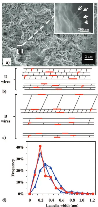
The UTS for the CNT-Cu wires are still noticeably higher, reflecting first that the presence of the CNTs hampers dislocation glide and that the dislocations pile-up at the CNT/Cu interface, producing less plastic deformation and second the strengthening role of the CNTs due to their high resistance to elongation[22]. A strong Cu-O-C interface would favor charge transfer. Ductile fracture was observed for all wires (Fig. 4a). CNTs are seen protruding from the fracture surface (inset inFig. 4a), which may reveal some degree of pull-out. Their frac-ture could be along the “sword-sheath” mode[22]. The UTS values tend to increase upon the decrease in wire diameter, reflecting the finer mi-crostructure, notably for the B samples. Interestingly, the UTS values are significantly higher for the CNT-Cu U wires than for the CNT-Cu B wires down to a diameter of 0.5 mm (771 MPa vs 676 MPa at 77 K, respectively).
By contrast, the thinner CNT-Cu B wires show ever higher UTS, reaching 876 MPa (77 K) for the 0.198 diameter. These are significantly better strength/conductivity combinations compared to Cu-based alloys ([4]and references therein). The UTS are 50% and 20% higher than for cryo-drawn Cu wires[8]and DWCNT-Cu wires[12], respectively. Such high UTS values at 77 K are interesting for non-destructive pulsed mag-nets operating in liquid nitrogen[23]. In the thinner wires, the elongat-ed Cu grain (lamella) width is of the order of the size of the dislocation cells (about 150–200 nm)[9]and it is assumed that the plasticity mech-anisms during wire-drawing are based on Orowan-type dislocation glide[24,25]. Assuming a homothetic deformation, it is reasonable to
assume that for the U wires, which originate from a powder and cylin-der with a uniform grain size, and whatever their diameter (Fig. 4b), the elongated Cu grains will have a relatively narrow lamella-width dis-tribution. By contrast, the B wires will retain a relatively wide size distri-bution until a certain wire diameter is reached, evaluated at about 0.5 mm, where the distribution will be similar to that for a U wire (Fig. 4c), with most grains about 150–200 nm in size. Moreover, it is im-portant to note that the larger Cu grains found in the B powder and cyl-inder will form upon drawing the B wires longer grains than those found in the U wires. In order to corroborate these hypotheses, the size (lamella width) of over 1000 grains was measured on EBSD grain size maps of longitudinal sections of selected wires. First, CNT-Cu U and B wires of the same diameter (0.506 mm) are compared (Fig. 4d). For the U wire (solid red circles inFig. 4d), the average lamella width is 0.28 μm (with d10, d50and d90equal to 0.06, 0.18 and 0.46 μm,
respec-tively) and for the B wire (solid blue triangles inFig. 4d), the average la-mella width is 0.34 μm (with d10, d50and d90equal to 0.12, 0.29 and 0.54
μm, respectively). Clearly, large grains are more abundant in the 0.506 mm B wire than in the 0.506 mm U wire. Then, the lamella-width distribution was calculated for a thinner (0.251 mm) B wire (open blue triangles inFig. 4d). The average lamella width is 0.26 μm (with d10, d50and d90equal to 0.05, 0.19 and 0.39 μm, respectively).
These values are fairly similar to that for the 0.506 mm U wire. These re-sults strongly support our hypotheses. We propose that in the early stages of wire-drawing, i.e. for wire diameters above about 0.5 mm, the presence of the larger Cu grains still predominates in B wires and only the limited portion of smaller Cu grains contribute to Orowan
Fig. 2. a) EBSD inverse pole figure maps of the transverse section (CNT-Cu B cylinder); (b) EBSD inverse pole figure maps of the longitudinal section (CNT-Cu B cylinder); c) EBSD grain size maps of the transverse section showing grains (black) and twins (red) (CNT-Cu B cylinder); d) EBSD inverse pole figure maps of the transverse section (0.506 mm CNT-Cu B wire); e) EBSD inverse pole figure maps of the longitudinal section (0.506 mm CNT-Cu B wire). f) TEM bright-field image of the longitudinal section of the (0.506 mm CNT-Cu U wire). (For interpretation of the references to color in this figure legend, the reader is referred to the web version of this article.)
strengthening, accounting for the lower UTS and lower resistivity com-pared to the U wires. In the latter stages, i.e. for wire diameters below about 0.5 mm, the previously larger Cu grains in B wires are now more elongated and the accompanying nanostructuration accounts for the steep increase in UTS (N20%) whereas for U wires further strength-ening is not possible anymore, most grains having already reached the dislocation cell size. Moreover, as noted above, the larger grains end up significantly longer than those originating from the smaller ones and are devoid of CNTs, therefore producing only a small increase in resistivity.
In conclusion, a bimodal distribution of the Cu grain size in Cu and CNT-Cu wires prepared by a combination of spark plasma sintering and RT wire-drawing favors high strength while limiting the increase in electrical resistivity.
The authors thank L. Datas and L. Weingarten for assistance in elec-tron microscopy, performed at “Centre de microcaractérisation
Raimond Castaing — UMS 3623” (Toulouse). The authors are grateful to Dr. G. Rikken for useful discussions. This work was performed under contract NANO2C from Université de Toulouse and Région Midi-Pyrénées (APR-2012-12050646) and contract ANR 2011-NANO-025 TRI-CO.
References
[1] R.Z. Valiev, R.K. Islamgaliev, I.V. Alexandrov, Prog. Mater. Sci. 45 (2000) 103–189.
[2] J. Schiøtz, K.W. Jacobsen, Science 301 (2003) 1357–1359.
[3] Y. Champion, C. Langlois, S. Guérin-Mailly, P. Langlois, J.-L. Bonnentien, M.J. Hytch, Science 300 (2003) 310–311.
[4] Y. Champion, Y. Bréchet, Adv. Eng. Mater. 12 (2010) 798–802.
Fig. 3. Electrical resistivity at 77 K (a), ultimate tensile strength at 293 K (b) and 77 K (c) versus wire diameter. Cu (○) and CNT-Cu (●) U wires; Cu (△) and CNT-Cu (▲) B wires. Data for OFHC-Cu (□) is from[9]. UTS uncertainty varies between ±0.02% for diameter 1.023 mm and ±0.5% for diameter 0.198 mm.
Fig. 4. a) SEM images of the fracture surface of the CNT-Cu U wire 0.506 mm in diameter. The inset shows a higher magnification image were protruding CNTs (arrowed) are observed; b) schematic description of the grain size distribution in the U wires assuming a homothetic deformation by wire drawing; c) same for the B wires. Red lines symbolize CNTs; d) lamella width distributions calculated from EBSD grain size maps for the 0.506 mm CNT-Cu U wire (●), 0.506 mm CNT-Cu B wire (▲) and 0.251 mm CNT-Cu B wire (△). (For interpretation of the references to color in this figure legend, the reader is referred to the web version of this article.)
[5] L. Lu, Y. Shen, X. Chen, L. Qian, K. Lu, Science 304 (2004) 422–426.
[6] Y. Zhang, Y.S. Li, N.R. Tao, K. Lu, Appl. Phys. Lett. 91 (2007) 1–3.
[7] K. Han, R.P. Walsh, A. Ishmaku, V. Toplosky, L. Brandao, J.D. Embury, Philos. Mag. 84 (2004) 3705–3716.
[8] A. Kauffmann, J. Freudenberger, H. Klauß, V. Klemm, W. Schillinger, V.S. Sarma, L. Schultz, Mater. Sci. Eng. A 588 (2013) 132–141.
[9] C. Arnaud, F. Lecouturier, D. Mesguich, N. Ferreira, G. Chevallier, C. Estournès, A. Weibel, A. Peigney, C. Laurent, Mater. Sci. Eng. A 649 (2016) 209–213.
[10] S.H. Risbud, Y.-H. Han, Scr. Mater. 69 (2013) 105–106.
[11] K. Hanazaki, N. Shigeiri, N. Tsuji, Mater. Sci. Eng. A 527 (2010) 5699–5707.
[12]C. Arnaud, F. Lecouturier, D. Mesguich, N. Ferreira, G. Chevallier, C. Estournès, A. Weibel, C. Laurent, Carbon 96 (2016) 212–215.
[13] C. Guiderdoni, E. Pavlenko, V. Turq, A. Weibel, P. Puech, C. Estournès, A. Peigney, W. Bacsa, C. Laurent, Carbon 58 (2013) 185–197.
[14]A. Kasperski, A. Weibel, C. Estournès, C. Laurent, A. Peigney, Scr. Mater. 75 (2014) 46–49.
[15] H. Wang, H. Zhang, Y. Hu, F.-C. Wang, S.-L. Li, E. Korznikov, X.-C. Zhao, Y. Liu, Z.-F. Liu, Z. Kang, Sci. Rep. 6 (2016) 26258.
[16] K.T. Kim, J. Eckert, S.B. Menzel, T. Gemming, S.H. Hong, Appl. Phys. Lett. 92 (2008) 121901.
[17] R. Sule, P.A. Olubambi, I. Sigalas, J.K.O. Asante, J.C. Garrett, Powder Technol. 258 (2014) 198–205.
[18] Z.H. Zhang, F.C. Wang, S.K. Lee, Y. Liu, J.W. Cheng, Y. Liang, Mater. Sci. Eng. A 523 (2009) 134–138.
[19] D.A. Hughes, N. Hansen, Acta Mater. 45 (1997) 3871–3886.
[20] D.P. Field, B.W. True, T.M. Lillo, J.E. Flinn, Mater. Sci. Eng. A 372 (2004) 173–179.
[21] K.T. Kim, S.I. Cha, T. Gemming, J. Eckert, S.H. Hong, Small 4 (2008) 1936–1940.
[22] M.F. Yu, O. Lourie, M.J. Dyer, K. Moloni, T.F. Kelly, R.S. Ruoff, Science 287 (2000) 637–640.
[23] J.T. Wood, J.D. Embury, M.F. Ashby, Acta Mater. 45 (1997) 1099–1104.
[24] L. Thilly, O. Ludwig, M. Véron, F. Lecouturier, J.P. Peyrade, S. Askénazy, Philos. Mag. A 82 (2002) 925–942.
[25] M. Huang, P.E.J. Rivera-Díaz-del-Castillo, O. Bouaziz, S. van der Zwaag, Scr. Mater. 61 (2009) 1113–1116.