ةيبعشلا ةيطارقميدلا ةيرئازجلا ةيروهمجلا
République Algérienne Démocratique et Populaire
Ministère de l'Enseignement Supérieur et de la Recherche Scientifique
UNIVERSITÉ FERHAT ABBAS – SETIF 1
FACULTÉ DE TECHNOLOGIE
SE
È
TH
Présentée au Département d’Electronique
Pour l’obtention du diplôme deDOCTORAT
Domaine : Sciences et Technologie
Filière : Electronique Option : Systèmes Embarqués et
Technologie Par
MEDKOUR Hicham
ME
È
TH
Conception et Réalisation d’Antennes Reconfigurables
Soutenue le 04 / 07 / 2019 devant le Jury :KRIM Fateh Professeur Univ. Ferhat Abbas Sétif 1 Président
ZEGADI Ameur Professeur Univ. Ferhat Abbas Sétif 1 Directeur de thèse
AIDEL Salih Professeur Univ. Mohamed El Bachir
El Ibrahimi de BBA Examinateur
People's Democratic Republic of Algeria
Ministry of Higher Education and Scientific Research
Ferhat Abbas University of Setif 1
Faculty of Technology
Thesis
Presented at the Department of Electronics
For the award of the degree of
DOCTORATE
Field: Sciences and Technology
Specialty: Electronics Option: Embedded Systems and
Technology By
Hicham MEDKOUR
itle
T
Design and Implementation of Reconfigurable Antennas
Defended on the 4th July 2019 before the Jury:
KRIM Fateh Professor Ferhat Abbas Univ. of Setif 1 President
ZEGADI Ameur Professor Ferhat Abbas Univ. of Setif 1 Supervisor
AIDEL Salih Professor Mohamed El Bachir El
Ibrahimi Univ. of BBA Examiner
Abstract
In this thesis we describe novel approaches in designing reconfigurable antennas. The proposed reconfigurable layouts are intended for integration into compact UWB communication systems and are characterized by their low profile and easy fabrication processes. Initially, the project was to design et implement some reconfigurable antennas based on conductive polymers. As a result, the first part of this thesis provides an advanced literature survey as well as an investigation on the use of tunable permittivity or conductivity in designing antennas based on conductive polymers. The second part of this thesis reports on the design of planar reconfigurable UWB antennas with interference filtering capabilities. Firstly, a planar monopole UWB reconfigurable antenna has been designed showing filtering capabilities in three narrow bands which could potentially interfere in this particular region of the spectrum. Reconfigurability allows the antenna to match to any interference cases. The presented design uses low-cost FR 4 substrates known for being light. Secondly, an extremely compact UWB single-sided reconfigurable designed antenna is described. Unlike the previous antenna, the reconfigurable filtering circuit has been exclusively implemented in the ground plane rather than in the radiating patch in order to optimize the radiation performance of the antenna. By doing so, the new design is cost effective, allowing interferences’ filtering at the antenna level rather than at a later stage and avoids complex biasing control antenna circuitry.
:ناونعلا
ت
ةلكيهلا ةداعلإ ةلباق صئاصخ تاذ تايئاوه ةعانصو ميمص
صخلم
تايئاوه ميمصت يف ةديدج قئارط انفصو ةلاسرلا هذه يف مكحتلل ةلباقلا صئاصخلا تاذ . تايئاوهل ميماصت ميدقت مت دقف نيب ةرصحنملا قاطنلا ةعساو تاددرت وذو مجحلا ةريغصلا تلااصتلاا ةمظنأ يف جامدلإل ةبسانم 3 و 10 GHz هذه زيمتت . .عينصتلا ةلوهسو ةيذاج لقلأا ةيئايزفلا ةئيهلا امه نيتماه نيتيصاخب تايئاوهلا لاصأ لا ةيادب يف رن انك ،عورشم بغ ىلإ ميمصت و عنص .ةلصوملا تارميلوبلا ىلإ اًدانتسا نيوكتلا ةداعلإ ةلباقلا تايئاوهلا ضعب ساسلأا اذه ىلع هذه نم لولأا ءزجلا رفوي ، لا لاسر ميمصت يف ةيلصوملا وأ طبضلل ةلباقلا ةيحامسلا مادختسا لوح ةسارد ىلإ ةفاضلإاب بدلأل اًمدقتم اًحسم ة تايئاوهلا لامعتساب .ةلصوملا تارميلوبلا تايئاوه ميمصت نع ًاريرقت ةلاسرلا هذه نم يناثلا ءزجلا مدقي UWB ةداعلإ ةلباقلا ةيوتسملا بطقلا يداحأ ليكشتلا ةداعلإ لباق يئاوه ميمصت مت ،ًلاوأ .لخادتلا ةيفصت تايناكمإ عم ليكشتلا UWB ةيفصتلا تايناكمإ راهظلإ يف ثلاث ملا فيطلا ةقطنم يف لخادتت نأ نكمي ةقيض تاقاطن .لخادت تلااح يأ عم قباطتلاب يئاوهلل نيوكتلا ةداعإ حمست .ةنيع زئاكر مدقملا ميمصتلا مدختسي FR 4 .ةفيفخ اهنوكب ةفورعم ةفلكتلا ةضفخنم ،ًايناث ةقدب ممصم يئاوه فصوي UWB يداحأ تلا ةداعلإ لباق بناجلا مكح ةداعلإ ةلباقلا حيشرتلا ةرئاد ذيفنت مت ،قباسلا يئاوهلا فلاخب . تلا مكح ىوتسملا يف رصحلا هجو ىلع امم ةفلكتلا ضفخنم ديدجلا ميمصتلا نوكي ،كلذب مايقلا .يئاوهلا عاعشإ ءادأ نيسحت لجأ نم عشملا حيحصتلا نم ًلادب يضرلأا .زيحتلا يف مكحتلا يئاوهل ةدقعملا رئاودلا بنجتيو ةقحلا ةلحرم نم ًلادب يئاوهلا ىوتسم ىلع تلاخادتلا حيشرتب حمسي تاملكلا ةيحاتفملا : لا ؛تايئاوه ؛ةعوبطملا لقاونلا UWB ةيئابرهك ةيلقان تاذ نئادل ؛ ؛ ةيلاع ةلكيهلا ةداعإ .Titre :
Conception et Réalisation d’Antennes Reconfigurables
Résumé
Dans cette thèse, nous décrivons de nouvelles approches dans la conception d'antennes reconfigurables. Les schémas reconfigurables proposés sont destinés à être intégrés dans des systèmes de communication UWB compacts et se caractérisent par leur profil bas et leurs processus de fabrication faciles. Au départ, le travail consistait à concevoir et à mettre en œuvre des antennes reconfigurables à base de polymères conducteurs, par conséquent, la première partie de cette thèse propose une étude bibliographique avancée ainsi qu'une étude sur l'utilisation de la permittivité ou de la conductivité accordables dans la conception d'antennes à base de polymères conducteurs. La deuxième partie de cette thèse porte sur la conception d’antennes UWB planes reconfigurables dotées de capacités de filtrage aux interférences. Premièrement, une antenne reconfigurable UWB monopolaire plane a été conçue, montrant des capacités de filtrage dans trois bandes étroites susceptibles d’interférer dans cette région spectrale. La reconfiguration permet à l'antenne de s'adapter à tous les cas d'interférences. La conception présentée utilise des substrats à faible coût de FR 4 connus pour leur légèreté. Deuxièmement, Nous décrivons une seconde reconfigurable antenne UWB et qui est extrêmement compacte. Contrairement à l'antenne précédente, le circuit de filtrage reconfigurable a été mis en œuvre exclusivement dans le plan de masse plutôt que dans le patch rayonnant afin d'optimiser les performances de rayonnement de l'antenne. La nouvelle conception est peu coûteuse et permet de filtrer les interférences au niveau de l’antenne plutôt qu’à un stade ultérieur, en évitant le besoin aux circuits complexes de commande de polarisation.
Acknowledgments
I first thank ALLAH, the Almighty, who lights us the right way.
I would like to express my sincere gratitude to everyone and organisations whose support, skills and encouragement were crucial to the successful completion of this thesis.
This work has been conducted in the laboratory: Croissance et Caractérisation de Nouveaux Semiconducteurs (LCCNS), Electronics Department, Technology Faculty of Ferhat Abbas University of Setif 1.
First and foremost, I would like to convey my deep gratitude to my principal supervisor, Professor Ameur Zegadi for his constant support throughout my doctorate research time at the University of Ferhat Abbas Setif 1. His encouragement and critical comments are all essential factors that led me throughout my work.
I am so thankful to Professor Ahmed Zouaoui, head of the laboratory, for his support.
I would like to mention my previous teacher and supervisor in Master’s degree, Professor Hamimi Chemali. He has not only inspired me the research passion but also helped me to balance it with my social life and professional progress.
I am also deeply indebted to Professor Tan-Phu Vuong and all the technical staffs at the Institute of Microelectronics Electromagnetics and Photonic in Grenoble who received me and allowed me to carry out my experimental work. Special thanks are due to Miss Erika Vandelle who has patiently helped me in the antenna fabrication and measurement processes as well as during the papers writing.
I thank Professor Fateh Krim, at Ferhat Abbas University of Setif 1, for having accepted to chair the jury of this thesis, I am very honoured.
I extend my warmest thanks to Professor Salih Aidel of Mohamed El Bachir El Ibrahimi University of Bordj Bou Arreridj and Dr. Chemseddine ZEBIRI, MCA at Ferhat Abbas University of Setif 1 for having accepted to be part of the jury of this thesis as examiners.
My doctorate research would not be possible without the assistance from the University of Ferhat Abbas Sétif 1, the faculty of Technology, from which I received financial support for my
short training stay abroad. Indeed, I would like to thank the administrative team, including the head of the department Professor Abdelouahab Hassam.
Throughout my doctorate, I have received valuable help from many friends and colleagues. I would like to thank Dr. Ali Mansoul from the Development Centre of Advanced Technologies (CDTA) in Algiers, Dr. Idris Messaoudene from National School of Computer Science in Algiers,
Dr. Abou Djamal form the University of Science and Technology Houari Boumediene in Algiers. I will never forget the fruitful assistance I received from Dr. Adam Narbudowicz from the Dublin Institute of Technology in Ireland. I wish to acknowledge my deep appreciation to my dear friends and doctorate colleagues Abdelbaset Laib and Imededdin Djadour who have always been to my side in any case and supported me unconditionally.
Last but not least, I would like to give my infinite love and appreciation to my father, my mother, my brothers and sisters for their infinite care and encouragement.
Hicham Medkour,
February 2019,
Page i
List of Acronyms
AC Alternative Currents
BST Barium Strontium Titanate
CSRR Complementary Split Ring Resonators
CCo Carbon coated Cobalt
CPW Coplanar Waveguide
CST Computer Simulation Technology
DMS Defected Microstrip Structure
DFX Drawing Interchange Format or Drawing Exchange Format
DC Direct Current
DGS Defect Ground Structure
FR Flame Retardant
HFSS Higher Frequency Spectrum Simulator
IMEP Institut de Microélectronique Electromagnétisme et Photonique
ITU International Telecommunication Union
LCP Liquid Crystal Polymer
MWCNT Multiwall Carbon Nanotubes
MSA Microstrip Antenna
MIMO Multiple Input Multiple Output
MgO Magnesium Oxide
MEMS Micro-Electro-Mechanical System
NASA National Aeronautics and Space Agency
PIN P-Intrinsic-N
POE Polyolefin Elastomer
PANI Polyaniline
PET Polyethylene Terephthalate
PPy Polypyrrole
PCB Printed Circuit Board
Page ii
PEDOT Poly(3,4-ethylenedioxythiophene)
PEDOT:PSS Poly(3,4-ethylenedioxythiophene): Polystyrene sulfonate
RCS Radar Cross Section
RF Radio Frequency
RFID Radio Frequency Identification
SMA Sub-Miniature version A
SRR Split Ring Resonator
WIMAX Wireless Interoperability Medium Access
WBAN Wireless Body Area Network
WLAN Wireless Local Area Network
UWB Ultra-Wide Band
VNA Vector Network Analyser
Page iii
List of Figures
General Introduction
1. Flow diagram of the followed research road map to achieve the final objective 5
Chapter 1
1.1 MSA array with reconfigurable polarization [3]
91.2 Single coupled feed MSA with reconfigurable polarization [4]
91.3 LC-based microstrip patch antenna [5]
101.4 BST based frequency reconfigurable antenna [13]
101.5 BST based frequency reconfigurable antennas [14]
111.6 BST base frequency reconfigurable antennas [15]
111.7 Frequency reconfigurable microstrip antenna [16]
131.8 Selective frequency reconfigurable monopole planar antenna [17]
131.9 Radiation pattern reconfigurable microstrip antenna [18]
141.10 Multi-beam radiation pattern reconfigurable microstrip antenna [19]
151.11 Reconfigurable polarization microstrip circular patch antenna [20]
151.12 Reconfigurable polarization square ring circular microstrip antenna [21]
161.13 Frequency and radiation pattern Reconfigurable MPA [22]
171.14 Frequency and radiation reconfigurable antenna MPA [23]
181.15 Frequency and polarization reconfigurable proximity coupled fed MPA [24]
191.16 Frequency and polarization reconfigurable MPA [25]
201.17 Pattern and polarization reconfigurable MSA [26]
211.18 Pattern and polarization Reconfigurable MSA [25]
221.19 3D view of the design of a microstrip antenna with reconfigurability of
frequency, radiation pattern and polarization [26]
221.20 Two mechanically flexible antennas realized in PEDOT: PSS [30]
241.21 Recent published antennas based on conductive polymers
251.22 A reconfigurable planar antenna with two patch edges in
conductivity-adjustable materials [41]
26Chapter 2
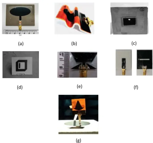
2.1 Chemical structures of typical conductive polymers
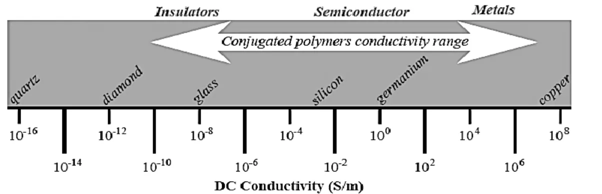
342.2 DC electrical conductivity range of some materials
342.3 Chemical structures of: (a) Polypyrrole (PPy); (b)
Page iv
2.4 Effect of PPy sheet thickness on the gain and radiation efficiency of
microstrip antenna [13]
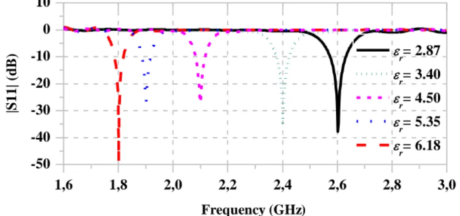
382.5 Frequency variation in accordance with the tuning dielectric constant [13]
392.6 Design concept of conductive polymer and tunable substrate based
microstrip antenna
392.7 Reflexion coefficient for different values of the dielectric constant
402.8 Relationship between the radiation efficiency and MSA resonance
frequency
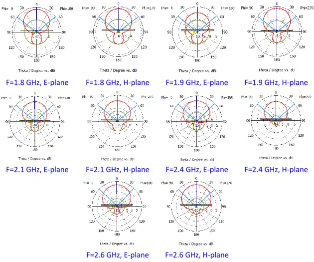
412.9 Simulated patterns in E- and H- planes at various frequencies
41Chapter 3
3.1 Perpetual notching UWB antennas
453.2 Five perpetual notches UWB antenna [4]
463.3 Dual reconfigurable notched band [5]
473.4 Compact dual notched band reconfigurable UWB antenna [6]
473.5 Dual notched band reconfigurable UWB antenna [7]
483.6 Triple notched bands reconfigurable UWB antenna with ideal switches [8]
493.7 First designed antenna basis structure
503.8 Design of the slots (S1, S2 and S3) to produce the filtering functions
513.9 Impact of slots parameters optimization on the notch performance
513.10 Insertion of ideal switches to control current circulation around the slots
523.11 Surface current distribution with ideal switches
523.12 Modification of the initial structure for filtering functions purposes
533.13 Transmission line model of the antenna including the diodes equivalent RLC
circuit
543.14 Design of the separation slots at the radiating patch and ground plane
553.15 Simulation results of reflexion coefficients
573.16 CST Surface current distributions of the antenna with real switches and the
biasing circuit being considered
583.17 Radiation patterns as simulated in CST
593.18 Radiation patterns simulated in CST
593.19 Frequency dependence of obtained antenna gain
60Chapter 4
Page v
4.2 Single layer UWB MEMS reconfigurable antenna [2]
664.3 Single layer UWB optically reconfigurable antenna [3]
674.4 Single layer UWB optically reconfigurable antenna [4]
674.5 Design and modification of the basis UWB single layer structure
684.6 Optimization of the slots’ dimensions
694.7 Implementation of the slots in the basis UWB structure
704.8 CST simulations show the optimization process of the slots’ dimensions
714.9 Switching configuration cases of the antenna
724.10 Surface current distribution of at the notched frequencies.
734.11 Simulation results of the antenna according to an ideal switching case
744.12 The insertion of S-parameter files using CST design studio
744.13 Antenna schematic assumed in the case of real control circuit of the filtering
functions
754.14 Simulated results obtained assuming real switches
754.15 Antenna schematic after the insertion of the filtering control slots and the
biasing arms
754.16 Comparative performances between ideal and real switches
754.17 Simulated current distribution assuming real switches
774.18 The fabricated prototype with RF components and SMA
784.19 Reflexion coefficient measurements using a Vector Network Analyser (VNA)
794.20 Measured and simulated frequency dependence of |S11|
794.21 Radiation performance measuring in the anechoic chamber
804.22 Radiation patterns at notch frequencies
814.23 Radiation patterns out of the notch frequencies
814.24 Simulated distribution of the gain as function of the frequency for the four
Page vi
List of Tables
Chapter 1
1.1 Physical properties of some conductive parameters 26
Chapter 2
2.1 Dimensions of the rectangular microstrip antenna 40
Chapter 3
3.1 Summary of the eight operational states of the antenna 55
3.2 Comparison of performance to literature 61
Chapter 4
4.1 Ideal switching configuration cases 73
Contents
Abstract صخلم Résumé Acknowledgements List of Acronyms iList of Figures
iii
List of Tables
vi
Contents
General Introduction
1
1. Advantages of Reconfigurable Antennas 2
2. Challenges in Reconfigurable Antennas 2
3. Benefits of Conductive Polymers based Antennas 3
4. Challenges of Conductive Polymers based Reconfigurable Antennas 4
5. Thesis Road Map 4
6. Thesis Layout 6
Bibliography 6
Chapter 1. State of the Art of Reconfigurable Antennas
7
1.1 Copper based Reconfigurable Microstrip Antennas
8
1.1.1 Reconfiguration through Tunable Material substrates
8
1.1.1.1 Polarization Reconfigurability using Liquid Crystals
Substrates
8
1.1.1.2 Frequency Reconfiguration using Ferroelectric BST
Substrates
Contents
1.1.2 Reconfiguration through Conductor Modification using PIN
Diodes
12
1.1.2.1 Frequency Reconfiguration using PIN diode
12
1.1.2.2 Radiation Patterns Reconfiguration using PIN diode
13
1.1.2.3 Polarization Reconfiguration using PIN diode
15
1.1.2.4 Frequency/Radiation Pattern Reconfigurable Antennas
16
1.1.2.5
Frequency/Polarization Reconfigurable Antennas
using PIN Diodes Switches
18
1.1.2.6
Pattern/Polarization Reconfigurable Antennas using
PIN Diodes Switches
20
1.1.2.7
Frequency/Pattern/Polarization Reconfigurable MSA
using PIN Diodes Switches
22
1.2 Conductive Polymers based Microstrip Antennas
23
1.3 Conductive Polymers based Reconfigurable Microstrip Antennas
26
1.4 Conclusion
27
Bibliography
27
Chapter 2. Conductive Polymers Basics & Reconfigurable Antennas
Concepts
322.1 Background
33
2.2 Electrical and Mechanical Properties of Conductive polymers
33
2.3 Electromagnetic Properties of Conductive Polymers
35
2.4 Frequency Reconfigurable MSA with CP Radiators
37
2.4.1
Reconfiguration Principles
38
2.4.2
Design in CST
39
2.4.3 Simulation Results
40
2.5 Conclusion
42
Bibliography
42
Chapter 3. Reconfigurable Monopole UWB Antenna with Triple
Filtering Functions
44
Contents
3.2 Design of the Basis Monopole Structure
49
3.3 Filtering Implementation
50
3.4 Filtering Control with Ideal Switches
52
3.5 Control of the Filtering using Real Switches
53
3.6 Simulation Results
56
3.7 Comparison to Previous Designs
60
3.8 Conclusion
61
Bibliography
62
Chapter 4. Reconfigurable UWB CPW-Antenna with Two Notched
Bands
64
4.1
Literature Review
65
4.2
Basis Structure of the Proposed Design
68
4.3
Implementation of the Notches
70
4.4
Reconfiguration with Ideal Switches
72
4.5 Reconfiguration with Real Switches using PIN diodes
74
4.6 Prototyping
78
4.7 Measurements and Discussion
78
4.7.1 Measurements of the Reflexion Coefficient |S
11|
79
4.7.2 Radiation Performance Measurements
80
4.8
Conclusion
82
Bibliography
83
Thesis Conclusion
84
Appendixes
87
Appendix A
Antenna Parameters
88
Appendix B
PIN Diode
91
Appendix C
Scientific Production
93
General Introduction
Page 2 General Introduction
1. Advantages of Reconfigurable Antennas
Assigning different antennas for each wireless protocol in a single device is no longer the best solution. There is an increased call today for further size miniaturization of wireless communication devices and henceforth the limited available space has to be shared carefully. Separate antennas of type monopole or microstrip are typically used in these devices and in many cases they may not have multiple-frequency capabilities. Generally, multiple antennas are integrated on a single device in order to enhance its reception capabilities but in sending mode only single antenna is used. Transmission from a portable device to a base station is the weakest mission in bidirectional communication links because of movability constraints like power, size, and cost. The portable handsets are commonly working in unexpected and rough electromagnetic environment which affects and decreases antenna performances. As a solution, antenna reconfigurability provides substantial help to deal with this problem. Tuning antenna’s operating frequency could be utilized to change operating bands, filtering interfering signals, or allowing antenna to accommodate with new unexpected working environments. In addition, antenna radiation pattern reconfiguration permits to focus maximum radiation power into privileged directions and therefore use less power for transmission and consequently extends battery life. Besides the two previous alternative options, reconfigurable polarization provides also several possibilities to a single antenna to perform transmission/reception through multiple types of polarization including horizontal/vertical linear polarizations and left/right hand circular polarizations. At present, low-profile and miniaturization are two highly desirable characteristics in today’s communication handsets and so the adoption of reconfigurable antennas would certainly respond to these requests through processing and managing these two properties. Hence, reconfiguration would assure additional operational freedom degrees in terms of adaptation, functionality and versatility.
2. Challenges in Reconfigurable Antennas
The integration of new features into conventional antennas presents not only a real challenge in terms of norms but certainly would arise several questions about cost, technology and efficiency [1]. The addition of antenna reconfigurability induces extra design complexities in control system implementation. These challenges should not only cover production of the desired levels of antenna functionality but also the integration of this new smart feature into a 1. Advantages of Reconfigurable Antennas
Page 3 General Introduction complete cost-effective system. The overall design system cost of the antenna will be largely balanced by the associated technologies for implementing this valuable reconfiguration.
The complete antenna functionality task requires dedicated signal processing and feedback circuitry and will certainly face further complications when adding different components. However, if a single reconfigurable antenna could deliver the same functionality of more than one traditional single-purpose system, significant savings in cost, weight, volume, and maintenance/repair resources may be realizable. Of course, integrating new kinds of functionality into antennas will not automatically result in higher or comparable performance and lower costs. System designers need to be willing to exploit these new degrees of freedom and functionality so that the antenna becomes a more active part of the communication link, working together with new circuits, signal processing techniques, communication and radar protocols. The difficulty lies also in the fact that reconfigurable antennas often take on non-canonical forms and there is interaction between closely spaced elements. The influence of switches and their biasing lines is a real problem and basically their behaviour is quite difficult to be predicted.
3. Benefits of Conductive Polymers based Antennas
For such important wireless applications like RFID (radio frequency identification), WBAN (wireless body area network) antennas are required with low-profile, light weight, compact size (xy-plane), resistant to deformation and robust to electromagnetic impact. Antennas made of conventional materials such as metals and ceramics do not satisfy the aforesaid characteristics. In the last few years, many researches have been performed on conductive polymers and eventually they have showed very interesting electrical and mechanical properties which are a very promising for application in antennas designing [2]. Conductive polymers such as Polypyrrole (PPy), Graphene, Polyaniline and PEDOT expose these highly potential assets. In addition to their high electrical conductivity, high mechanical elasticity and being light, they can be implemented easily at a low-cost. Furthermore, they have low density and are highly resistant to corrosion with their production process is friendly to environment. Henceforth, there is high motivation to take advantage from their interesting properties to produce flexible, low-cost and easily foldable antennas and hence be able to produce reconfigurable antennas based on conductive polymers owing to the fact that the electrical conductivity of conductive polymers is adjustable [3].
Page 4 General Introduction
4. Challenges of Conductive Polymers based Reconfigurable Antennas
It is desirable to take advantages of the properties of conductive polymers in designing reconfigurable antennas. This combination would result into the development of highly efficient, multi-functional, low-cost and conformal antennas. Reconfigurability enhances the functionality of the antenna and multiplies its operating capabilities while the properties of conductive polymer. However, the challenge in today’s reconfigurable conductive polymer antenna designs lie in how to integrate a robust reconfiguration mechanism onto the polymer antenna structure. Experimentally, there are two kinds of used polymer substrates: rigid and flexible substrates. In the last decade, there have been significant advances in the development of conductive polymer using rigid substrates. It is easy to integrate different control mechanisms onto conductive polymer surfaces, which are deposited on rigid substrates to achieve not only the frequency reconfiguration but also adjust the radiation pattern or polarization. However, the task is practically difficult when it comes to the integration of reconfigurability in flexible and plastic based substrate antennas. For instance, it is hard to associate lumped components (RF switches) onto conductive polymers that are deposited on plastic substrates. Furthermore, for the case of wearable antennas’ applications, the presence of lumped elements on top of the polymer antenna represents a risk of being detached due to repeated physical deformations, which are possible in a realistic human-body environment (e.g. bending, stretching and twisting), and also when washing. Hence, the robustness of flexible reconfigurable conductive polymer antennas is a research challenge to find the right substrate that will be convenient to reconfiguration mechanisms.
5. Thesis Road Map
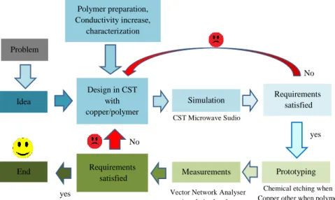
The objective of this thesis is to develop some antennas that offer certain additional functionalities while providing better performances to meet today’s requirements and/or to solve certain problems linked to some wireless applications. The road map undertaken is as illustrated
in Fig. 1. There are two main axes we started with:
1. The synthesis of a conductive polymer;
2. The design and implementation of some reconfigurable antennas.
In the first path, an experimental investigation has been carried out on preparing and characterizing some samples of conductive polymers in our laboratory (LCCNS). During a period of time, chemical polymerization of pyrrole was done and polypyrrole (PPy) has been 5. Thesis Road Map
Page 5 General Introduction synthesised. The measurement of the conductivity using the method of four points has shown that the samples had low electrical conductivity. However, this requird additional chemical processing to enhance the electrical conductivity which is a crucial parameter for the antenna. Nevertheless, the tasks of conductivity enhancement, characterization of the polymer and the exploration of its interaction with electromagnetic environment are postponed and left as future work due to the lack of characterization facilities. Herein, we confined ourselves to give only the state of the art on antennas and reconfigurable antennas based on conductive polymer. Still, we present a theoretical study on conductive polymer properties with particular attention given to their electromagnetic behaviour.
In the meantime, work has been carried out in the second axe in which reconfigurable antennas based on copper were investigated. The objective is to come up with compact reconfigurable antennas that are capable to deal with the problem of interference that suffer some wireless systems in the electromagnetic spectrum 3.1 to 10 GHz. Indeed, two reconfigurable monopole antennas have been conceived, simulated and optimized using the commercial software CST [4]. In the first antenna conception, our work was limited to the design, the simulation and the optimization. While in the second, in addition to the simulation study the antenna was fabricated and its performances were measured.
Figure 1. Flow diagram of the followed research road map to achieve the final objective. 5. Thesis Road Map
Requirements satisfied Idea Problem Design in CST with copper/polymer Simulation Measurements Requirements satisfied End Prototyping yes No No yes CST Microwave Sudio
Chemical etching when Copper other when polymer Vector Network Analyser
Anechoic chamber
Polymer preparation, Conductivity increase,
Page 6 General Introduction
6. Thesis Layout
The thesis is divided into four chapters:
Chapter 1: contains some highlights on the state of the art of reconfigurable antennas. We review recent works that have been conducted on reconfigurable microstrip antennas using different reconfiguration mechanisms in planar structures. A particular attention is given to published literature on conductive polymer antennas and on the efforts being done in designing reconfigurable antennas based on conductive polymers.
Chapter 2: a review on the electrical and mechanical properties of conductive polymers is presented as well as their behaviour in electromagnetics media. The preliminary simulation results of an antenna conception based on conductive polymers are discussed. The frequency reconfiguration through the use of tuning permittivity was also investigated.
Chapter 3: include the design of a reconfigurable monopole ultra wideband antenna. The results thus obtained are discussed in the light of current literature.
Chapter 4: discusses and presents the results of the second ultra-wideband antenna conception. We also report on the steps taken in implementing experimentally the antenna. We present the results on the antenna performances.
Bibliography
[1] N.O. Parchin, H.J. Basherlou, Y.I. Al-Yasir, R.A. Abd-Alhameed, A.M. Abdulkhaleq, J.M. Noras, “Recent Developments of Reconfigurable Antennas for Current and Future Wireless Communication Systems”, Electronics 8(2), p.128, 2019.
[2] S.J. Chen, "Flexible, Wearable and Reconfigurable Antennas based on Novel Conductive Materials: Graphene, Polymers and Textiles", PhD dissertation, Adelaide University Australia, 2017.
[3] R.L. Haupt, “Reconfigurable Patch with Switchable Conductive Edges”, Microwave Opt.
Technol. Lett., 51(7), pp. 1757-1760, 2009.
[4] https://www.cst.com. 6. Thesis Layout
State of the Art of
Reconfigurable Antennas
ECONFIGURABLE antennas have been a dynamic field of research during the last two decades in which the motivation is to provide antennas with additional functionalities and better performance. We aim in this introductory chapter to give an overview on the state of the art of reconfigurable microstrip antenna based on both copper and conductive polymers. Radiation properties of a microstrip antenna are strongly linked to the geometry and substrate material of the antenna. The sizes of the radiating patch in one hand control the resonance frequency and in the other hand; the resonance frequency is inversely proportional to the relative permittivity and permeability of the substrate. Besides, the operating bandwidth is technically proportional to the substrate electrical height. This is the principle of reconfiguration which has been recently proposed in microstrip antennas and which will be reviewed in this chapter. The reconfiguration based on frequency, radiation pattern and polarization will be discussed.
R
Page 8
Chapter 1
1.1 Copper based Reconfigurable Microstrip Antennas
Reconfiguration of a microstrip antenna can be achieved through two methods. The first consists of modifying the dimensions of the radiating elements (patch/ground plane) and therefore metallic stubs or slots can be add to reduce or extend the dimensions of the current surfaces. While the second method lays on modifying the parameters of the dielectric substrate such as the high or the permittivity or permeability. In this case, tunable materials based on dielectric are used as substrates which can be controlled through an external effect like light, temperature, electric/magnetic field, etc…
1.1.1 Reconfiguration through Tunable Material substrates
1.1.1.1
Polarization Reconfigurability using Liquid Crystals SubstratesLiquid crystals are auspicious materials in microwave engineering since they have emerged as potential materials for applications in antenna technologies [1-2]. Liquid crystal (LC) materials have been used to construct a planar antenna with reconfigurable polarization [3]. As shown in
Fig 1.1, the design proposed consists of 22 dual-fed microstrip patch array and two distinct
feeding systems for each feeding of the dual-fed antenna. The design is capable of switching between dual circular and dual linear polarizations according to the variance phase shift between feedings networks of the antenna. The feeding systems are realized in inverted microstrip line topology with the liquid crystal material as a tunable substrate. When altering the liquid crystal, the differential phase shift is acquired between the feeding systems. Additionally, due to the continuous change of the LC material, the polarization can be switched between linear and circular polarizations. This antenna operates at 13.75 GHz which is in Ku and W frequency bands since LC materials decrease the dielectric losses which makes it suitable for applications at higher frequencies. Another microstrip patch antenna with reconfigurable polarisation was proposed in
[4]. As demonstrated in Fig 1.2, a tuneable coupled line loaded with liquid crystal-based varactors is used to reconfigure the polarization of the antenna. Therefore, when a bias voltage is applied, the proposed antenna can be continuously reconfigured to give circular or linear polarization. The prototype is validated by simulation and measurements. Tuneable liquid crystals based dielectric substrate is investigated again for the development of frequency reconfigurable microstrip antenna as proposed in [5].
Page 9
Chapter 1
Figure 1.1. MSA array with reconfigurable polarization [3]. (a) schematics of the single
radiating element and explode d perspective and (b) bottom view; (c, d) pictures of the fabricated antenna form the top (left) and bottom (right)views.
Figure 1.2. Single coupled feed MSA with reconfigurable polarization [4].(a) top view; (b) and
(c) cross section views; (d) photograph of the fabricated prototype (dimensions: G1= 0.3 mm,
G2= 0.1 mm, L1= 0.7 mm, L2 =1.8 mm, W1=0.6 mm).
The proposed design is illustrated in Fig 1.3. Reconfiguration is achieved by applying a low frequency AC bias voltage. The amplitude of the external applied electric field panels the tilt angle of the crystal liquid molecules which in turns work as directors that changes the constitutive properties of the LC dielectric material. Hence, various bias voltage values that varies between 0 and 10 Volts are applied continuously, helped to tune the antenna frequency range between 5.45 and 5.84 GHz.
1.1 Copper based Reconfigurable Microstrip Antennas
(a) (b) (c) (d)
(a) (c) (d)
Page 10
Chapter 1
Figure 1.3. LC-based microstrip patch antenna [5].
1.1.1.2 Frequency Reconfiguration using Ferroelectric BST Substrates
Barium Strontium Titanate (BST) ceramic belongs to ferroelectric materials whose relative permittivity can be tuned by applying different voltages. Because of their high permittivity, BST materials have been utilized as substrates to achieve size reduction in different types of antenna such as dielectric resonator antennas.In recent years, BST has appealed for significant attention owing to its potential of low dielectric loss and high tunability [6-7]. It has been useful in several microwave devices, such as compact sized antennas [8-9], phased array antennas [10], and reconfigurable antennas based on BST varactors [11-12]. The structure shown in Fig 1.4 is a frequency reconfigurable microstrip antenna with a wide instantaneous operation band based on BST/MgO composite films [13]. The objective of adding MgO to BST composite is to efficiently dilute the permittivity and keep a considerable dielectric tunability. The frequency reconfigurability is attained by changing the permittivity of BST film, and an extra Fabry-Perot resonant structure is adopted to increase the instantaneous operation band. As a result, a wide instantaneous band that is closely 26% superior is acquired in measurement, which means that the working band of this antenna can be tuned from 9.9–13.5 GHz to 10.9–14.2 GHz.
Figure 1.4. BST based frequency reconfigurable antenna [13]. (a) The original reconfigurable
model and (b) the modified instantaneous wideband reconfigurable model.
Page 11
Chapter 1
This antenna is highly suitable for wireless communication systems due to its attractive feature of instantaneous frequency reconfigurable. The geometry shown in Fig 1.5 shows another frequency reconfigurable microstrip antenna for which BST substrate material is adopted again
[14]. The relative permittivity of BST material used in this design is approximately 100, and a thin BST film of 0.3 mm is used as the primary substrate. A tuneable bias voltage is applied between the metal patch and the ground plane to control the relative permittivity of BST material. As a consequence, the antenna frequency resonance is tuned of 10% from 13.3 to 14.7 GHz by changing the bias electric field from 0 to 10 V/µm. Nguyen et al. proposed a compact frequency reconfigurable planar antenna based on ferroelectric (BST) TiO3 thin films [15].
Figure 1.5 BST based frequency reconfigurable antennas [14]. (a) Side view; h=0.3 mm, the
thickness of the Taconic Layer: ht =1 mm; (b) the top view of the antenna: WaLa rectangular
aperture arranged on the ab top surface of the PCB layer, and a (Ls + a - x0)Ws feed line
arranged on the bottom side.
Figure 1.6. BST base frequency reconfigurable antennas [15]. (a) schematic of the notch
antenna; (b) the varactor based on BST thin film.
1.1 Copper based Reconfigurable Microstrip Antennas
Page 12
Chapter 1
As shown in Fig 1.6 the notch antenna is loaded with a variable metal/insulator/metal (MIM) capacitor and is achieved by a monolithic method. The design delivers frequency tunability rate of 14.5% under an electric field of 375 kV/cm.
1.1.2 Reconfiguration through Conductor Modification using PIN Diodes
Altering the conductors shape and dimensions of planar/microstrip antenna (MSA) affect considerably the antenna radiation properties. This aspect is used as the basis to reconfigure the antenna operating frequency, bandwidth, pattern, and polarization. Basically, the modifications in the radiating patch or ground plane alter in fact the normal current distributions and contribute to other new current maps which change the antenna radiation properties. Therefore, if one can objectively control the current distribution it becomes possible to control the radiation properties of the antenna which becomes reconfigurable. There are different kinds of switches used to control current circulation in microstrip antennas, among which there are PIN diodes.
1.1.2.1. Frequency Reconfiguration using PIN Diode
The microstrip slot antenna proposed in [16] is capable to change its frequency between nine distinct narrow bands from 1.98 to 3.59 GHz.The configuration of the antenna is shown in
Fig 1. 7. It is fabricated on a Taconic RF-35 dielectric substrate with a thickness of 3.04 mm
having a permittivity of 3.5. It includes a rectangular patch and a slotted ground-plane beneath it. The design of the slot under the patch delivers extra operating bands to the antenna. Five PIN diodes are used to control the length of the slot which help to switch the operating frequency between nine different frequencies from 1.98 to 3.59 GHz. The antenna has a dimension of 5050 mm2. The frequency switchability of this antenna makes it suitable for cognitive radio
applications. The antenna proposed in [17] is a monopole microstrip antenna with a slotted ground plane, shown in Fig 1.8. It consists of an inverted U-shape radiating patch fed by a microstrip line and a rectangular ground plane underneath. The radiating element offers a wide operating band between 2.63 and 3.7 GHz. Additionally, four horizontal slots were inserted in the ground plane to help the antenna to resonate at four different resonant narrow bands. To switch between the four narrow band frequencies, the slot’s lengths are controlled using PIN diodes. The fabricated prototype has a size of 6851 mm2 and offers an omnidirectional radiation pattern. This antenna is suitable for cognitive radio applications.
Page 13
Chapter 1
Figure 1.7. Frequency reconfigurable microstrip antenna [16]. (a) top view on patch; (b) the
bottom view on the modified ground plane. Dimensions (mm) a= 6.4, b=13, c = 13.95, d= 16, e=18, g=15.38, S1 to S5 are PIN diodes.
Figure 1.8. Selective frequency reconfigurable monopole planar antenna [17]. (a) top view on
patch; (b) the bottom view on the modified ground plane. Dimensions (mm) a= 6.4, b=13, c = 13.95, d= 16, e=18, g=15.38, S1 to S5 are PIN diodes.
1.1.2.2. Radiation Patterns Reconfiguration using PIN Diode
A microstrip antenna was proposed in [18] to operate at the WiMAX frequency range 3.44 to 3.6 GHz with the capability to reconfigure its radiation pattern. As seen in Fig. 1.9, the antenna is designed on dielectric substrate with a permittivity of 3.5 and thickness of 3 mm. A circular
1.1 Copper based Reconfigurable Microstrip Antennas
Page 14
Chapter 1
coaxially feed patch is on the upper side of the substrate with four quasi-rectangular radiation elements coupled to the patch using PIN diodes in symmetrical positions. The radiation pattern reconfiguration is achieved by switching the state of the four PIN diodes and thus, the antenna main beam can be switched between 𝜑 = 0°, 𝜑 = 90°, 𝜑 = 180° or 𝜑 = 270° while 𝜃 = 30°. Four different radiation patterns state can be performed at WiMAX band. Besides, the proposed configuration has a small size and very acceptable realised gains which is more than 8 dBi. A similar reconfigurable radiation pattern microstrip antenna is proposed in [19], shown in Fig. 1.10.Circular patches surrounded by four other parasitic circular patches are printed on the upper side of Taconic substrate of 2.2 permittivity and a thickness of 1.6 mm. The ground plane is printed on the lower side of the substrate which has a full size of 120120 mm2.The surrounding
parasitic patches are shorted to the ground plane using four pins named S1, S2, S3 and S4. Four PIN diodes are used to connect the four shorting pins to each one of the parasitic patches. The parasitic patches work as director/reflectors which are controlled by the switching of the PIN diodes and as such, beam reconfiguration is achieved. Hence this antenna can switch its main radiation pattern into nine different directions: (𝜑, 𝜃) = (0°, 0°), (0°, 23°), (45°, 22°), (90°, 24°), (135°, 22°), (180°, 24°). Besides, the antenna yielded a gain greater than 7 dB for the nine possible pattern configurations.
Figure 1.9. Radiation pattern reconfigurable Microstrip antenna [18]. (a) top view on patch;
(b) the bottom view on the modified ground plane. Dimensions (mm): a = 60°, G = 6.4, h= 3, Df
= 1.2, Rp = 5, R1 = 27.5, R2 = 7, R3 = 6, R4 = 5.3. 1.1 Copper based Reconfigurable Microstrip Antennas
Page 15
Chapter 1
Figure 1.10. Multi-beam radiation pattern reconfigurable microstrip antenna [19]. (a) top
view; (b) side view; (c) back view. Dimensions (mm): L=120, R= 23.7.
1.1.2.3. Polarization Reconfiguration using PIN Diodes
Polarization diversity can help to avoid fading losses caused by multipath effects. Therefore, there has been an increasing interest in implementing antennas with reconfigurable polarization. The design shown in Fig. 1.11 illustrates the structure of a microstrip antenna which is capable to alter its polarization between three types: linear, left-hand and right-hand circular polarizations [20]. The structure consists of circular patch printed on the top of Taconic substrate having the permittivity of 3.52 and a thickness of 1.52 mm. Two pairs of L-shape slits are created symmetrically along x and y axis on the patch edges. In order to activate and deactivate the electrical length of the slits, four different PIN diodes are placed at the open end of each slit. This approach helped to obtain reconfigurable polarization at the WLAN frequency band 2.4 to 2.48 GHz.
Figure 1.11. Reconfigurable polarization microstrip circular patch antenna [20].(a) top view;
(b) side view. Dimensions (mm): d= 5.5, h= 1.524, Lp= 15.3, r= 17.9, t= 0.035, W=55. 1.1 Copper based Reconfigurable Microstrip Antennas
(a) (b) (c)
Page 16
Chapter 1
A microstrip ring antenna with reconfigurable circular polarisation has been proposed [21]. Its geometry is shown in Fig. 1.12. It comprises a FR-4 substrate with dielectric constant of 4.2 and a thickness of 1.57 mm with an overall size of 7070 mm2. Square ring patches with a
T-shaped microstrip feed are printed on the top face of the substrate. A square loop is created at the centre of the ground plane on the lower face of the substrate.The antenna is fed by a gap-coupled through inductors across a distance g. Two gaps gap1 and gap2 are inserted in the patch and across which two PIN diodes are inserted to electrically connect/disconnect the two parts of the square ring. The reconfiguration of the polarization is achieved by controlling the switching states of the two PIN didoes at the frequency of 3.45 GHz. When diode 1 is ON and diode 2 is
OFF, the antenna resonates with a right-hand circular polarization. When diode 1 is OFF and
diode 2 is ON, the antenna resonates with a left-hand circular polarization. The obtained antenna gain was greater than 3 dBi.
Figure 1.12. Reconfigurable polarization square ring circular microstrip antenna [21].(a) top
view; (b) side view. Dimensions (mm): d2= 1, d2= 1, g=0.3, h= 1.6, L= 55, l1=10, l2=7.5, W = 55, t=
0.035, W=8.2, Wf= 3, Wt= 0.8, Ws=2.5.
1.1.2.4. Frequency/radiation pattern reconfigurable antennas
The slot microstrip antennas of [22] offers a reconfiguration capability in two ways: frequency and radiation pattern. As shown in Fig. 1.13, the antenna is designed on Taconic FR35 substrate with the permittivity of 3.5 and a thickness of 1.52 mm. The rectangular patch is on the top of the substrate while the slot ground plane is on the back. The slot in the ground plane generates a bidirectional radiation pattern, therefore, a metallic sheet is placed behind the antenna in order to produce a directional radiation pattern. Frequency reconfiguration is achieved by controlling the electrical length of the slot using two PIN diodes denoted S1 and S2. Thus, the
1.1 Copper based Reconfigurable Microstrip Antennas
Page 17
Chapter 1
antenna is capable to work at three distinct frequencies 1.82, 1.93 and 2.10 GHz. Radiation pattern reconfigurability is ensured through the introduction of four slits near to the corners of the ground plane. The control of the slits’ length helped to alter the angle of the main radiation beam of the antenna and as such, it became capable to tune the beam angle between 0°, +15° and −15° at each one of the operating frequency bands.
Figure 1.13. Frequency and radiation pattern reconfigurable MPA [22].(a) Top view; (b) side
view. Dimensions (mm): a= 130, b= 160, c= 33, d=21.75, e= 21.75, n=29, m=65.25, l=21.75,
k=3.2.
The antenna proposed in [23] is a microstrip antenna, shown in Fig. 1.14, featuring reconfigurability in frequency and in radiation pattern. It consists of small patch which is surrounded by a square ring called internal ring and in between are two PIN diodes D3, D4 to ensure switchable contacts. Both metallic parts are surrounded by another square ring named external ring. Again, two PIN diodes D1 and D2 connect the internal and external rings together. According to the switching states of the PIN diodes, the antenna is capable to operate in three distinct modes, with resonance frequencies: 2.84, 3.84 and 3.85 GHz. Meanwhile, radiation pattern changes in accordance with the diodes switching states.
• In mode 1, the antenna produces 3 dB beam width from −30° to 25° with 7.4 dBi of gain. • In mode 2, it provides 3 dB beam width from −80° to −15° with 5.7 dBi of gain.
• In mode three, it produces 3 dB beam from 5° to 60° with the maximal gain of 5.7 dBi.
1.1 Copper based Reconfigurable Microstrip Antennas
Page 18
Chapter 1
These results were checked through both numerical simulations and performance measurements of an experimental prototype.
Figure 1.14. Frequency and radiation reconfigurable antenna MPA [23]. Dimensions (mm): a=
4.6, b = 7, c= 28.5, d=40, L= 100.
1.1.2.5. Frequency/Polarization Reconfigurable Antennas using PIN Diode Switches
In some antenna designs, the objective was to combine reconfigurable frequency with reconfigurable polarization in a single microstrip antenna structure. The proximity coupled fed configuration proposed in [24] consists mainly of a rectangular patch printed on Neltec N9000 substrate with a permittivity 2.2 and a thickness 0.762 mm, shown in Fig. 1.15. In order to implement the frequency reconfiguration feature, an additional small patch is positioned next to the central patch and connected to each other through a PIN diode. Frequency reconfiguration is established in the following way:
▪ When the diode is switched OFF, the antenna frequency resonance is due to only the central patch which resonates at the first band 5.7 GHz.
▪ When the diode is switched ON, the antenna resonance is due to both central and small patches and thus another resonant band at 5.2 GHz is produced.
To get polarization reconfigurability at either of two operational bands, each corner is cut off from the main and additional patches are inserted through a narrow L-shaped cut to generate polarization reconfigurability. A couple of PIN diodes named D1, D2, D3, D4, D5, D6 and D7 are employed to control the polarization of the antenna. Hence, to produce a circular polarization at 5.2 GHz, the pair of small parasitic patches placed diagonally is coupled to the main patch by
Page 19
Chapter 1
switching ON the two corresponding diodes and therefore, by changing the diagonal pair of small patches the polarization can be altered between left-hand circular polarization and right hand-circular polarization. Furthermore, the antenna is capable to offer hand-circular polarization at the higher band 5.7 GHz when the additional patch is connected to the main patch and two small parasitic patches at the diagonal ends are disconnected from the circuit. This disconnection serves to generate two orthogonal components of currents which yields a circular polarization at 5.7 GHz.
Figure 1.15. Frequency and polarization reconfigurable proximity Coupled fed MPA [24].Top
and side views. Dimensions (mm): g = 0.3, gb = 0.3, Ib = 65, Ipb = 17.8, Laddb = 4, If =28, Wb =60,
Waddb =18.15, Wpb = 18.15, Wf= 2.4, Wt= 0.58, Isb =2.2, It = 11.9.
Another example of frequency and polarization reconfigurabilities in microstrip antennas has been proposed recently [25]. The diagram is shown in Fig. 1.16. The antenna is realized on Rogers 5880 substrate of permittivity 2.2 and a thickness of 3.175 mm. The structure is composed of a square patch, three groups of switchable shorting pins (group 1, group 2, group 3) connected to the ground plane, and four controllable perturbation pads coupled to the corner of the patch through PIN diodes D1, D2, D3 and D4. The antenna is fed by a coaxial probe through a microstrip line. Polarization reconfigurability is achieved by controlling the switching state of
Page 20
Chapter 1
the four PIN diodes. When the two diodes in the opposite direction (D1 & D2 or D3 & D4) are switched ON, the two orthogonal modes will be split in resonant frequency with equal amplitude and 90° phase difference which can yield a circular polarization. When all the four PIN diodes are turned ON, linear polarization can be generated from the symmetrical structure of the antenna. Hence, by governing the states of the diodes D1-D4, the polarization of the antenna can alter the polarization between left-hand, right-hand and linear. The antenna operating frequency can be switched between eight distinct narrow bands by properly shorting the patch to the ground plane via the three groups of the shorting pins which are controlled by the PIN diodes.
Figure 1.16. Frequency and polarization reconfigurable MPA [25]. (a) top view; (b) bottom
view. Dimensions (mm): d = 1, d1 = 12, d2 = 20, d3 = 28, W1 = 4, W2 = 3, Wp = 48, L1 =33, L2 = 12.
1.1.2.6. Pattern/Polarization Reconfigurable Antennas using PIN Diode Switches
The compact microstrip antenna proposed in [24] offers reconfigurability of both radiation pattern and polarization. The antenna, shown in Fig 1.16, comprises two truncated monopoles arranged orthogonally and connected to the microstrip lines via ideal switches named S1 and S2. It is intended for applications in 2.4 GHz IEEE 802.11 WLAN and Bluetooth bands. Radiation pattern and polarization reconfiguration can be conducted through the tow switches S1 and S2. At state 1, when S1 is switched ON and S2 is OFF, the vertical monopole is excited (parallel to the y axis). Hence, the antenna radiation is maximally on xz-plane and null along positive and negative y axis. At state 2, S1 is switched OFF and S2 is ON, the horizontal monopole is exited (parallel to x axis). In this case, the maximum radiation is along yz-plane and null along the positive and negative x axis. Meanwhile, polarization also can be reconfigured into horizontal or
1.1 Copper based Reconfigurable Microstrip Antennas
Page 21
Chapter 1
vertical since, in state 1, the antenna provides linear polarization on the y axis, whereas in state 2, it provides also linear polarization but on the x axis.
Figure 1.17. Pattern and polarization reconfigurable MSA [24]. (a) top; (b) back view.
Dimensions (mm): Wg = 10, Lg = 10, Ls = 6.75, L = 19, W = 19, Ws = 3, Gs = 1.2, W1 = 0.8, L1 = 8, L2 = 3, L3 = 9, L4 = 2, h = 1.6.
A circular microstrip patch antenna with reconfigurable pattern and polarization was proposed [25]. As shown in Fig. 1.18, the antenna includes a circular patch whose structure is changeable trough PIN diode switches used to control radiation patterns and polarization. The antenna is fed by two coaxial ports carefully positioned orthogonally to maintain simultaneous radiation patterns and high isolation between the ports. Fourteen PIN diodes (switches D1), located radially on the antenna, are forwardly biased and used to dynamically change the radius of the circular patch and thus, alterations in the shape of the radiation pattern are attained by exciting different electromagnetic modes in the antenna structure. Four PIN diodes (switches D2) are reversely biased and connect or disconnect two perturbation segments to the inner circular patch. Therefore, the antenna can offer three different types of polarization:
❖ When both switches D1 and D2 are switched OFF, the antenna offers an elliptical polarization.
❖ When the switches D1 are switched OFF and the switches D2 are switched ON, the antenna offers a linear polarization with the mode TM21.
1.1 Copper based Reconfigurable Microstrip Antennas
Page 22
Chapter 1
❖ When the switches D1 are switched ON and the switches D2 are switched OFF, the antenna offers a linear polarization with the mode TM31.
Figure 1.18. Pattern and polarization reconfigurable MSA [25].Top and side views. Dimensions
(mm): a= 130, b =160, c= 33, d=21.75, e=21.75, n=29, m=65.25, l=21.75, k=3.2.
1.1.2.7. Frequency/Pattern/Polarization Reconfigurable MSA using PIN Diodes Switches
The main challenge in today’s antenna designs is to come up with a single microstrip antenna structure that is capable to produce reconfigurability in the three radiation properties all together.
Still, a modified structure of microstrip antenna which is capable of independently reconfigure the operating frequency, the radiation pattern and the polarization has been proposed
[26]. The configuration, shown in Fig. 1.19, comprises two layers of Rogers RO4003 substrates. The first layer supports the driver element, which is a square patch which is fed coaxially. The second layer carries a parasitic metallic surface subdivided into pixels with their biasing control circuits. The parasitic pixels are interconnected by PIN diodes.
Figure 1.19. 3D view of the design of a microstrip antenna with reconfigurability of frequency,
radiation pattern and polarization [26]. Dimensions (mm): lp= 12, sp=3, hp= 1.5, ld=wd=31,
hd=3, It=240, wt=120, d=variable.
(a) (b)
Page 23
Chapter 1
The activation of a specific switch configuration of pixels generates the suitable geometry over the metallic surface to deliver the required reconfigurable antenna properties. The antenna simultaneously reconfigures its operation frequency over a 25% frequency range, steers the radiation pattern beam over E and H planes, and switches between four different polarizations
1.2 Conductive Polymers based Microstrip Antennas
A variety of antennas based on different types of conductive polymers have been reported in the literature, from optically transparent to opaque, rigid to flexible, and narrow-band to UWB. In this context, it is worth mentioning the very first antenna designs based on conductive polymers.
The earliest reported transparent polymeric antennas were presented by National Aeronautics and Space Agency (NASA) in 1997 [27], namely including two antennas working at 2.3 and 19.5 GHz based on a transparent conductive dioxide polymer AgHT-8. This work has showed the feasibility of transparent and conformal antennas design based on polymeric materials, despite the fact that the antennas were not flexible.
A four-element crossed dipole direction-finding antenna assembly based on a fabric realized in S2 glass fibres with Polypyrrole (PPy) coating layer was reported in 1999 [28]. This design used PPy rather than metal to reduce the antenna radar cross section (RCS) to gain corrosion resistance and to exploit adjustable electromagnetic properties, by smartly taking advantage of the relative low conductivity (from 10 to 100 S/m) in the PPy coating. Avoiding metals in the design is due to two reasons.
• Firstly, metals are heavy and have a very high metallic conductivity leading to a large RCS due to the strong incident wave reflection;
• Secondly, low antenna efficiency is acceptable or can be compensated.
However, this concerned a very special application, and more generally highly conductive conductors are naturally a common requirement for the majority of antenna design, so as to achieve high antenna efficiency. Because of the relatively low conductivity and the process-limited thickness, antennas based on conductive polymers usually have low efficiencies. For instance, Cichos et al. [29] represented a performance study of polymer-based RFID antennas working at 13.56 MHz for a short communication range. The experimental results from this study demonstrated that antennas realized with conductive polymer pastes achieved approximately only half of the real range of its corresponding copper antenna. This can be straightforwardly
Page 24
Chapter 1
attributed to the higher ohmic losses, and it was also demonstrated that the read range can be improved by increasing the paste thickness and by using lamination.
Two dipole antennas based on PEDOT:PSS for RFID applications were proposed by Kirsch et al. [30], shown in Fig. 1.20.These were realized on polyethylene terephthalate (PET) substrate using modified PEDOT:PSS ink patterned with screen printing and inkjet printing technologies. The antennas exhibited a light weight and an excellent mechanical flexibility, but a lower gain (2 to 6 dB lower) than the copper ones, due to the very limited achievable printed polymer thickness and the low film quality.
Figure 1.20. Two mechanically Flexible Antennas realized in PEDOT:PSS [30].
The same authors have also conducted a performance study of similar polymeric dipole antenna in multiple-input multiple-output (MIMO) systems. They concluded that the antenna yields approximately half of that of copper due to the relatively low conductivity [31-32].
Verma et al. [32] and Kaufman et al. [33] investigated the effect of film thickness, respectively, on the radiation efficiency of 4.5 GHz PPy patch antenna and for an UWB antenna. They confirmed that sufficient film thickness is crucial for antenna efficiency. The efficiency of antenna based on lossy conductors like conductive polymer can be strongly dependent on the antenna radiation characteristics. For example, a resonant antenna such as slot antenna will have a lower antenna efficiency compared to a non-resonant antenna such as a leaky-wave antenna, since the resonance process will typically build up a higher current density and thus cause higher ohmic losses in the conductor. Especially when the conductor has a thickness well below a skin depth and a relatively low conductivity, the discrepancy between antenna types can be significant. As an example, an UWB antenna realized using a PPy film was reported by Kaufmann et al. yielding an antenna efficiency of nearly 80% [34]. The UWB antenna, shown in
![Figure 1.1. MSA array with reconfigurable polarization [3] . (a) schematics of the single](https://thumb-eu.123doks.com/thumbv2/123doknet/2956433.80928/26.892.160.836.158.366/figure-msa-array-reconfigurable-polarization-schematics-single.webp)
![Figure 1.6. BST base frequency reconfigurable antennas [15] . (a) schematic of the notch](https://thumb-eu.123doks.com/thumbv2/123doknet/2956433.80928/28.892.189.789.860.1057/figure-bst-base-frequency-reconfigurable-antennas-schematic-notch.webp)
![Figure 1.8. Selective frequency reconfigurable monopole planar antenna [17] . (a) top view on](https://thumb-eu.123doks.com/thumbv2/123doknet/2956433.80928/30.892.201.750.597.869/figure-selective-frequency-reconfigurable-monopole-planar-antenna-view.webp)
![Figure 1.15. Frequency and polarization reconfigurable proximity Coupled fed MPA [24]](https://thumb-eu.123doks.com/thumbv2/123doknet/2956433.80928/36.892.309.630.358.753/figure-frequency-polarization-reconfigurable-proximity-coupled-fed-mpa.webp)