-] A2’I
ç/?t,
__,Université de Montréal
ARM Processor Modeling
at a Cycle Accurate Level in SystemC
Par:
Hongmei Sun
Départrnent d’informatique et de recherche opérationnelle
faculté des arts et des sciences
Mémoire présenté à la Faculté des études supérieures
en vue de l’obtention du grade de
Maître ès Sciences (M. Sc.)
en informatique
Avril,
2003Université
de Montréal
Direction des bibliothèques
AVIS
L’auteur a autorisé l’Université de Montréal à reproduire et diffuser, en totalité ou en partie, par quelque moyen que ce soit et sur quelque support que ce soit, et exclusivement à des fins non lucratives d’enseignement et de recherche, des copies de ce mémoire ou de cette thèse.
L’auteur et les coauteurs le cas échéant conservent la propriété du droit d’auteur et des droits moraux qui protègent ce document. Ni la thèse ou le mémoire, ni des extraits substantiels de ce document, ne doivent être imprimés ou autrement reproduits sans l’autorisation de l’auteur.
Afin de se conformer à la Loi canadienne sur la protection des renseignements personnels, quelques formulaires secondaires, coordonnées ou signatures intégrées au texte ont pu être enlevés de ce document. Bien que cela ait pu affecter la pagination, il n’y a aucun contenu manquant.
NOTICE
The author of this thesis or dissertation has granted a nonexclusive license allowing Université de Montréal to reproduce and publish the document, in part or in whole, and in any format, solely for noncommercial educational and research purposes.
The author and co-authors if applicable retain copyright ownership and moral rights in this document. Neither the whole thesis or dissertation, nor substantial extracts from it, may be printed or otherwise reproduced without the author’s permission.
In compliance with the Canadian Privacy Act some supporting forms, contact information or signatures may have been removed from the document. While this may affect the document page count, it does not represent any loss of content from the document.
Ce mémoire intitulé:
ARM
Processor Modeling
at a Cycle Accurate Level in SystemC
Présenté Par:
Hongmei Sun
A été évalué par un jury composé des personnes suivantes:
Jean Pierre David
Président-rapporteur
lMostaphaAbou1hamid
Directeur de recherche
François-R Boyer
CôZffiiêcfir
-Marc Feeley
Membre du jury
Mémoire acceptéRésumé
La technologie de SimulationlMachine virtuelle est aujourd’hui une partie intégrale de beaucoup de systèmes de calcul. Un simulateur de matériel est un logiciel qui émule les dispositifs câblés spécifiques permettant l’exécution du logiciel qui est écrit et compilé pour ces dispositifs sur les systèmes alternatifs. L’ARM est un microprocesseur RISC 16/32-bit embarqué. Il possède un mécanisme de décalage intégré. L’adressage auto-indexé, les instructions load/store multiple et presque toutes les exécutions d’instructions conditionnels permettent au processeur ARM de réaliser un bon équilibre de haute performance, prix et faible consommation électrique, sur une aire de silicium réduite. L’ARM est largement répandu dans les communications portables, les ordinateurs de poche, le multimédia, produits de consommation numérique et solutions embarquées. Il n’existe pas un simulateur de micro-architecture ARM à source ouvert dans le domaine publique.
Dans ce mémoire, nous explorons différents types de stratégies de simulation (simulation au niveau architecture, exécution directe, recompilation dynamique, code chaîné, simulation d’ensemble d’instructions) et de leurs applications. Nous étudions également le comportement du pipeline du processeur ARM et combinons le comportement du pipeline du ARM [25][26] et celui du DLX [24] pour obtenir une description originale d’exécution de micro-architecture de ARM. En conclusion, nous construisons un simulateur cycle précis du processeur ARM (ARM-Simulator), qui simule la micro-architecture du processeur qui inclut un pipeline 5-stage, chemin d’expédition, la logique de couplage, etc. Ce simulateur est mis en application avec SystemC et des concepts de génie logiciel. Ainsi il est modulaire, facile à étendre, et intégré avec d’autres modules. C’est maintenant un projet autonome de logiciel, après encapsulation appropriée, il peut être un composant à brancher à un système d’application, pour simuler et évaluer la performance.
Le simulateur “modèle de noyau ARM” est validé par un simulateur de jeu d’instructions (ISS) ARM. Nous comparons les résultats du modèle de noyau ARM avec ceux de 115$
ARIVI pour nous assurer que le comportement du simulateur ARM est correct. Le code objet de l’ARM est généré par le compilateur croisé ARM-ELF-GCC. Celui-ci compile le code source C en code objet ARM sous le système d’exploitation Linux. Nous entreprenons également des expériences pour l’évaluation des performances.
Mots-clés: Simulation, Simulateur, Langues de simulation, Stratégies de simulation, Simulateur d’ensemble d’instruction, Microprocesseur RISC, Pipeline, Expédition, Couplage, Compilation croisée
111
Abstract
SimulationlVirtual machine teclmology is an integral part of many computing systems today. A hardware simulator is a piece of software that emuÏates specific hardware devices enabling execution of software that is written and compiled for those devices on altemate systems. ARM is a 1 6132-bit embedded RISC microprocessor. It has a built-in shifi mechanism. Auto-indexed addressing, loadlstore multiple instructions and almost ail instructions conditional execution allow the ARIvI processor to achieve a good balance of high performance, low cost, power efficient and low silicon area. ARM is widely used in portable communications, hand-held computing, multi-media, digital consumer and embedded solutions. There doesn’t exist an open source ARM micro-architecture simulator in public domain.
In this thesis, we explore different kinds of simulation strategies (Architecture level simulation, Direct Execution, Dynamic Recompilation, Threaded code, Instruction Set Simulation) and their applications. We also study ARIvI processor pipeline behavior, combine ARM pipeline behavior [25][26] and DLX pipeline [24] to obtain an original description of ARM micro-architecture implementation. Finally, construct a cycle accurate ARM processor simulator (ARM-Simulator), which simulates the micro-architecture of the processor that includes 5-stage pipeline, forwarding path, interlock logic, etc. This simulator is implemented with SystemC and software engineering concepts. So it is modular, easy to extend, and integrated with other modules. It is now a standalone software project, after appropriate encapsulating, it can be a component to plug into an application system, simulate and evaluate performance.
The simulator (ARM core model) is validated by an ARM Instruction Set Simulator (ISS). We compare the resuit from the ARM core model and the result from the ARM ISS, to know if the behavior of the ARM program is correct. The ARIVI object code is generated by ARM-ELF-GCC cross compiler. It compiles the C source code to ARM object code on the Linux operating system. We also conduct experiments for evaluating performance.
Keywords: Simulation, Simulator, Simulation Languages, Simulation Strategies, Instruction Set Simulator, RISC Microprocessor, Pipeline, Forwarding, Interlock, Cross Compile
V
Table of Contents
Résumé
j
&bstract
iii
1’able of Zontents
yList of ]‘ables
vii
List of Figures
viii
cronyIns
x
T”lotations
xii
Acknowledgement
xiii
Z hapter 1 Introduction
1
Chapter 2 Background
$
2.1 Overview of Simulation Strategies 8
2.2 Existing work for ARM processor simulator 9
Chapter 3
ARMProcessor Core
12
3.1 ARM Processor Architecture introduction 12
3.2 Processor Modes, Registers and PSRs (Program Status Register) 13
3.3 ARIVI instructions 18
3.4 Addressing Modes 21
3.5 Organization ofthe 5-stage ARM Pipeline 29
Chapter 4 Implementation of the
ARMcore model
33
4.1 Ail the Instructions operation in different stage (except IF) 33
4.2 Forwarding 41
4.3 lnteriock [24][25] 47
4.4 Branch instructions [25][26] 47
4.5 Some special instructions’ implementation 49
4.5.1 Load Multiple Registers (LDM) 49
4.5.3 Swap awordlbyte (SWP, SWPB) .52
4.5.4 Multiply instructions (MUL, MLA, UMULL, SMULL) 54
4.5.5 Long multiply and accumulate instructions (UMLAL, SMLAL) 55
4.6 Current and Saved Program Status Register (CPSR, SPSR) 57
4.7 Discussion on generalization 60
C hapter 5 ‘Sïalidation of the niodel
62
5.1 Methodology of Validation 62
5.1.1 The ARM core mode! 62
5.1.2 Validate the ARIvI core mode! with an ISS (Instruction Set Simulator) 64
5.2Experiments 67
5.3 Summaryofthis validation 6$
Zhapter 6 Performance Evaluation
70
C hapter 7 Conclusion
73
keferences
75Appendix A: Instructions implemented in this model
79
Appendix
B: ARMimplementation mode!, source code description
$1
vii
List of Tables
Table 2-l: Compare the existing ARIVI simulators and the ARIVI Core Model 11
Table 3-l: Processor mode description 14
Table 3-2: Registers [26] 16
Table 3-3: Condition code encoding [261 21
Table 3-4: Addressing mode 22
Table 3-5: Shift types 23
Table 3-6: Comparison ofARM architectureal pipeline depth 30
Table 4-1: Ail the instructions operation in different stage 34
Table 4-2: Work of every stage 38
Table 4-3: Destination register of corresponding pipeline register temporary data ALUOutput, D,
LMD (for the source instruction of the forwarding) 43
Table 4-4: Source register of pipeline register temporary data A, Bb, C (for the destination
instruction of the forwarding) 44
Table 4-5: Forwarding paths 44
Table 5-1: Programs for basic test 67
Table 5-2: Programs for combination test 68
List of Figures
Figure 3.1: ARIvI instruction set summary [26] 19
f igure 3.2: Multiplies and extraloadJstore instructions [26] 20
figure 3.3: Miscellaneous [26] 20
Figure 3.4: Addressing mode 1 data processing instruction binary encoding [26] 23
figure 3.5: LSL operation 24
figure 3.6: LSR operation 24
Figure 3.7: ASR operation 24
Figure 3.8: ROR operation 24
figure 3.9: ROX operation 24
Figure 3.10: Addressing mode 2 Single word and unsigned byte transfer instruction binary
encoding [26] 25
Figure 3.11: Addressing mode 3 Half-wordand signed byte transfer instruction binary
encoding [26] 26
Figure 3.12: Addressing mode 4 Multiple register transfer instruction binary encoding [26] ....28 Figure 3.13: Addressing mode 5 Coprocessor data transfer instruction binary encoding [26] ... 29
Figure 3.14: ARM 5-stage pipeline organization [25] 32
Figure 4.1: Forwarding paths 41
Figure 4.2: Instruction sequence for forwarding process 42
Figure 4.3: RAW hazard between two adjacent instructions 47
Figure 4.4: Insert a nop to avoid RAW hazard 47
Figure 4.5: Branch instruction operation 4$
Figure 4.6: LDM instruction operation 49
f igure 4.7: STM instruction operation 51
Figure 4.8: SWP instruction operation 53
Figure 4.9: Multiply-1 instruction operation 54
Figure4.10: Multiply-2 instruction operation 55
Figure 4.11: PSRs (progam status register) operation 57
ix
Figure 5.2: Validate the ARM core model. 64
f igure 5.3: A program executed on the ARM core model (without library) 65
figure 5.4: A program executed on ISS (with libranes) 65
Acronyms
AHB Advanced High performance Bus
ALU Arithmetic and Logic Unit
AMBA Advanced Microcontroller Bus Architecture
APB Advanced Peripheral Bus
ARM Acom Risc Machine
ASB Advanced System Bus
ASR Arithmetic Shift Right
CPI Clock cycles Per Instruction
DSP Data Signal Processing
EDA Electronic Design Automation
EXE EXEcution
FIQ Fast Interrupt reQuest
HDL Hardware Description Language
ID Instruction Decode
W Instruction Fetch
RQ Interrupt ReQuest
15DB Integrated Services Digital Broadcasting
ISS Instruction Set Simulator
LR Link Register
LSL Logical Shifi Lefi
LSR Logical Shifi Right
MEM MEMory access
OS Operating System
OSCI Open SystemC Initiative
PC Program Counter
PSR Program Status Register
RISC Reduced Instruction Set Computer
ROR Rotate Right
ROX Rotate Right with eXtend
SoC System on Chip
SP Stack Pointer
StepNP System level Telecom Experimental Platform for Network Processing
VCD Value Change Dump
VHSIC Very High Speed Integrated Circuit
VHDL VHSIC Hardware Description Language
WIF Waveform Intermediate format
WB Write Back
Notations
0x123 hex 123
]Rm..n sub range from ‘m bit’ to ‘n bit’ ofIR
logical shifi left
R[m] ‘bit m’ ofIR
mem[addr] content ofmemory in address ‘addr’
Regs[m] content ofregister Rm
mu! multiplier in figure 3.14
mux multiplexer in figure 3.14
% system prompt
O aspace
bold & underlined command line
xiii
Acknowledgement
Ibis work has been a challenging experience for me. I leamed many existing tecimologies. I received a lot of support and help from the professors and colleagues in our department.
I would like to thank Professor Fi Mostapha Aboulhamid, my director, and Professor françois-R Boyer, rny co-director, for their continued guidance, encouragement, enthusiasm, and support are greatly appreciated. Also great thanks to the colleagues for their encouragement and help.
Chapter 1 Introduction
Role of simulation in the design flow
Simulation / Virtuat machine technology [1] is an integral part of many computing systems today. Java, SirnOS [2][3] and VMware [for rnnning a complete OS as an application on another operating system], Connectix Virtual PC/Game station and Microsoft’s .NET are different examples of such systems. This technology is incredibly useful as a secure means for execution of untrusted software in a sandbox environment, and an ideal platform for code-development for new hardware devices.
A hardware simulator is a piece of software that emulates specific hardware devices, enabling execution of software that is written and compiled for those devices on alternate systems. The machines that are simulated will be referred to as target machines, and the system on which the simulator is actually rnnning is referred to as the host machine [4J.
Simulation at vanous levels of abstraction has played a key role in the design of computer systems. There are numerous compelling reasons for implementing simulators, most of them obvious. Design teams need simulators throughout ah phases of the design cycle.
1. Jnitially, during high-level design, simulation is used to narrow the design space and establish credible and feasible alternatives that are likely to meet competitive performance objectives.
2. Later, during microarchitectural definition, a simulator helps guide engineering trade-offs by enabling quantitative comparison ofvarious alternatives.
3. During design implementation, simulators are employed for testing, functional validation, and late-cycle design trade-offs.
4. Finally, simulators provide a useful reference for performance validation once real hardware becomes available.
Outside of the industrial design cycle, simulators are also heavily used in the computer architecture acadernic research cornmunity.
2
Some benefits ofusing simulators are:
1. Simulators are flexible and thus new features or components can easily be added. It is possible to model features, including those that might flot be possible to do on the hardware.
2. It allows stress testing ofprograms like operating systems by simulating complex interrupt and exception conditions.
3. Since simulators are built in software, they are more deterministic. The deterministic behavior of simulators makes programs execution reproducible, and thus helps in locating problems.
Primary applications of simulators consist of computer architecture studies and performance tuning of compiled software, and the compilation process itself. Various types of simulators exist, each addressing different aspects like dock cycle rate, modeling the microprocessor chip logic, modeling the program execution environment, etc.
StepNP (System-level Telecom Experimental Platfonn for Network Processing) is a modeling platform for multiprocessor and network processors, under development. The platform will help in performance evaluation, design exploration by changing architecture parameters such as interconnects, pipeline characteristics, instruction sets and memory schemes. The platform should be flexible and modular to allow a ‘plug, simulate and evaluate’ approach. This allows plugging different kinds of processors and interconnections to evaluate and create a new system. Core models include ARIVI processor [26] and DLX processor [24]. Jnterconnects models include the AMBA bus [2$] and different interconriect topologies such as chordal rings [5], crossbars, rings etc. The ARM core model implemented in this work was originally a component in this platform. Now it is a standalone project.
ARIVI is the industry’s leading provider of 16/32-bit embedded RISC microprocessor solutions. ARIVI’s microprocessor cores are high-performance, low-cost, power efficient. They are rapidly becoming the volume RISC standard in such markets as portable
communications, hand-heÏd computing, multimedia digital consumer and ernbedded solutions.
Simulation languages
Simulation allows faster development of design and cheaper and easier debugging during the design stage. Hardware description languages provide support for the simulation of concurrent processes and offer constructs to describe inter-process signal transfer. Iwo hardware simulation languages have become standard design entry tools for simulation and synthesis-Verilog [34] and VHDL [33]. While the results are very accurate the speed of simulation is very slow since they are more suitable for RT (Register Transfer) level design than for higher levels of abstraction. More powerful than these simulation languages are SystemC [35] and Superlog [32]. SystemC was launched by Synopsys and CoWare, it is backed by some 30 electronic design automation (EDA) vendors, which formed the Open SystemC Initiative (OSCI). This independent standards organization promotes SystemC as a coinmon digital ftamework that will streamiine product development for EDA synthesis tools. Superlog is another language for system-level design, developed by CoWare and based on Verilog and C. In this work, we implement an ARM processor simulator using SystemC to obtain an open source core of ARIVI which is cycle accurate and demonstrate the design flow of SystemC on a real example including validation.
SystemC [27] is a C++ class library and a methodology that we can use to effectively create a model of sofiware algorithms, hardware architecture, and interfaces of SoC (System On a Chip) and system-level designs. We can use SystemC and standard C++ development tools to create a system-level model, quickly simulate to validate and optimize the design, explore various algorithms, and provide the hardware and software development team with an executable specification of the system. SystemC supports hardware-software co-design and the description of the architecture of complex systems consisting of both hardware and software components. It supports the description of hardware, software, and interfaces in a C++ environment. The following features of SystemC allow it to be used as a co-design language:
4
1. Modules: SystemC has a notion of a container class caiied a module. This is a hierarchical entity that can have other modules or processes contained in it.
2. Processes: Processes are used to describe functionality. Processes are contained inside modules. SystemC provides tbree different process abstractions (method process, thread process, clocked thread process) to be used by hardware and software designers.
3. Ports: Modules have ports through which they connect to other modules. SystemC supports single-direction and bi-directional ports.
4. Signais: SystemC supports resoived and unresolved signais. Resolved signals (a bus) can have more than one driver whiie unresolved signais can have only one driver.
5. Rich set of port and signal types: To support modeling at different leveis of abstraction, from the functional to the RTL, SystemC supports a rich set of port and signal types. This is different than languages like Verilog that only support bits and bit-vectors as port and signal types.
6. Rich set of data types: SystemC has a rich set of data types to support multiple design domains and abstraction levels. The fixed precision data types aiiow for fast simulation, the arbitrary precision types can be used for computations with large numbers, and the fixed-point data types can be used for DSP applications. SystemC supports both two-valued and four-valued data types. There are no size limitations for arbitrary precision SystemC types.
7. Clocks: SystemC lias the notion of docks (as special signals). Ciocks are the timekeepers of the system during simulation. Multiple docks, with arbitrary phase relationship, are supported.
8. Cycle-based simulation: SystemC includes a cycle-based simulation kemel that aiiows high-speed simulation.
9. Multiple abstraction levels: SystemC supports untimed models at different levels of abstraction, ranging from high-level functional models to detailed dock cycle
accurate RTL models. It supports iterative refinement of high level models into lower levels of abstraction.
10. Communication protocols: SystemC provides multi-level communication
semantics that enable us to describe SoC and system 110 protocols with different levels for abstraction.
11. Debugging support: SystemC classes have run-time error checking that can be tumed on with a compilation flag.
12. Waveform tracing: SystemC supports tracing of waveforms in VCD, WIF, and ISDB formats.
Using the $ystemC approach, the designer does flot have to be an expert in multiple languages. SystemC allows modeling from the system level to RTL. The SystemC approach provides higher productivity because the designer can model at a higher level. Writing at a higher level can result in smaller code, which is easier to write and simulates faster than traditional modeling environments. Testbenches can be reused from the system level model to the RTL model saving conversion time. Using the same testbench also gives the designer a higher confidence that the system level and the RTL model implement the same functionality.
The objective ofthis research is to:
• Explore different kinds of processor simulator and their applications.
• Study ARM processor pipeline behavior, combine ARM pipeline behavior
[25][26] and DLX pipeline [24] to obtain an original description of ARM micro architecture implementation.
• Construct a cycle accurate ARM processor simulator with 5-stage pipeline (ARM Simulator). Which simulate the micro-architecture of the processor that includes 5-stage pipeline, forwarding path, interlock logic etc. Afier encapsulating, it will be a component of StepNP modeling platform, can be plugged, simulated and evaluated in different applications. The ARM core model is irnplemented by using
6
SystemC and software engineering concepts. So it is modular, easy to extend, and integrated with other modules.
• Validate the ARM core model using an ISS of ARIVI processor at instruction level. Because the ISS and the ARM core mode! do flot have the same precision, so we validate it at instruction level to ensure the behavior of ARM program is correct.
• Evaluate the performance ofthe cycle accurate ARM processor simulator.
This thesis is divided into seven chapters. Its content is organized as follows:
Chapter 2 provides background know!edge. At first, it gives an overview of simulation techniques, latter, it introduces the existing work for ARM processor simulator.
Chapter 3 introduces the ARIVI processor, ARM architecture, ARM instructions sets, addressing mode of different instructions and 5-stage pipeline organization.
Chapter 4 presents the implementation of the ARM core model. It introduces how to implement the 5-stage pipeline, the work of every pipeline stage for every instruction. Then, it explains the execution of forwarding, interlock and branch instructions. It also describes the execution of some special instructions. The details of this description can be considered as original since they are not described in the specification of the ARM. At last, it discusses the generalization ofthe model.
Chapter 5 describes the methodology for validating the model. The ARIVI core mode! is validated by an TSS (Instruction Set Simulator). Arm-e!f-gcc is the cross compiler that generates the arm object code. Then the object code is run on the ARM core model and ISS. By comparing the resuits from different model to know if the ARM core model is valid. Since ISS and the ARM core model (cycle accurate levels) do not have the same precision, so this validation is only from the instruction level. We also use some special
examples to validate the architecture of the processor core, includig functiona! units, forwarding path, inter!ock logic etc. Then it gives sorne experiments for validating it.
Chapter 6 introduces the ARM core model performance metrics. We do some experiments, compare the execution time ofISS and the ARM core model for the same workload, count the number of cycles and instructions so as to compare the compiled code quality from different compilers, calculate the CPI to evaluate the performance of an application system.
Chapter 7 concludes with the features of the mode! and the contributions of this thesis and then discusses future work.
Chapter 2 Backgrouncl
Cliapter 2 Background
This section gives an overview of simulation strategies and existing work for the ARIvI processor simulator.
2.1 Overview of Simulation Strategies
The best simulation method depends on the application of the simulation resuits. This section outiines several simulation strategies and their applications.
Architectural tevet Simulation [6117118]:
Logic designers build Architectural simulators to express and test new designs. These allow emulation of the different parts of a processor, using either the simple core, or the core and the data caches and other components. These are generally flot intended for executing target system binaries on aiternate piatforms, but rather to allow research into the modification ofthe internai data-paths ofthe processor.
Direct Executioit [1]:
Target machine binaries can be executed natively on the simulator host processor by encasing the program in an environment that makes it execute as though it were on the simulated system. This technique requires that either the host system has the same instruction set as the target, or that the program be recompiled for the host architecture. Instructions that cannot execute directly on the host are replaced with procedure calls to simulator code. This method is also known as Dynamic Recompilation [Dynarecs]. Native execution of the recompiled code leads to a much faster execution of the simulated software, but they have lengthy context switching, i.e. when the host processor has to switch to target processor. This may slow down the simulation.
Threaded Code [9][1O]:
This is a simulation technique where each op-code in the target machine instruction set is mapped to the address of some (lower level) code in the sirnulator system, to perform the
appropriate operation. This can be implemented efficiently in machine code on most processors by simply performing an indirect jump to the address, which is the next instruction. This method does not suffer from lengthy context switching.
htstruction set sim utators [4]:
Instruction set simulator [ISS] executes target machine programs by simulating the effects of each instruction on a target machine, one instruction at a time. The Instruction sets simulators are attractive for their flexibility: they can, in principle, model any
computer, gather any statistics, and run any program that the target architecture would mn. They easily serve as backend systems for traditional debuggers as well as architecture design tools such as cache simulators. A lot of temporal debuggers have recently started using ISS. An ISS can dispatch instructions by fetching from a simulated memory, isolating the operation code fields, and also branching, based on the values of these fields. Once dispatched, reading and manipulation of variables that represent the target system’s state are used to simulate the instmction’s semantics. They are flot cycle accurate since they do not take into account the iteming of an instruction pipelining.
2.2 Existing work for ARM processor simulator
There has been a lot ofresearch on software simulation ofthe ARM processor. These can be categorized according to the level of simulation, whether at the architectural level or the instruction set, or the techniques used, e.g. dynamic recompilation of parts of the simulated software to natively mn on the guest system.
Dynarecs [ARMphetamine]
ARMphetamine [1] and tARMac [11] are based on the direct compilation technique. They are fast and accurate ARIVI emulators. ARM code program segments are translated into native code as they are being emulated. A fetch-decode-execute emulator starts executing the ARM code, and when a specific block of the ARM code has been executed more times than a preset threshold, a translation routine is employed. This generates covers for each source instruction, i.e. chunks of native code that have the same semantics as the translated instructions. These covers are then executed every time the
10
translated biock of code needs to be run. The development platform for ARMphetamine and tARMac is linux/x86. They are open source, but flot cycle accurate, so can’t be used for performance evaluation.
Architecture tevet [$WARMJ[61
SWARM was designed as an ARM module to plug into the SimOS system developed at Stanford University. SimOS allows emulation of various parts of an ARM processor, using either the simple core, or the core and the caches. SWARM was intended flot for
running ARM binaries on an alternate piatform, but rather to allow research into the modification of the internai data-paths of the ARM processor. It implements a smali amount of internai co-processors at a basic level, and provides support for the full register/cache/external memory hierarchy. It does not take into account the micro-architecture of ARM processor core and the pipelining execution of an instruction.
Instruction Levet [SimARMJ[12J[13]
SimARM [12] is an instruction set simulator (ISS) that interprets ARM programs at the instruction level obviating the need for ARIvI hardware. ISSs are simpler to implement, but they are slower than simulators based on dynarecs due to the fact that ail instructions are strictly interpreted.
ARMulator [13] is anotherISS with a slight variation: it ensures identical cycle-count for instructions. This means that instructions take the same number of simulator’s cycles to execute as ifrun on real ARIvI hardware. This is important for precise simulation since some compilers can optimize code that takes advantage of the cycle-counts of specific instructions. But it is flot open source to the public, can’t be integrated into SystemC.
In this work, we implement the ARM Core Mode!, a cycle-accurate micro-architecture simulator. It simulates ARM instruction sets, and also simulates 5-stage pipeline (including hazard detecting, forwarding path, interlock logic and automatic no-op insert). It can act as an ISS to execute ARM program by simulating the behavior of the program. It is a modular design, so it can be integrated in SysternC, as a component can be plugged into an application system. It can also evaluate system performance by counting the
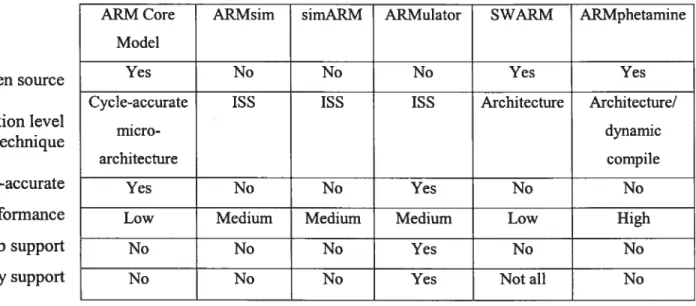
number of cycles for executing a program; it can also compare the quality of code compiled by different compilers. It also takes into account ail the pipeline effects such as hazard detecting, data forwarding, interlock, automatic no-op inserting etc. Table 2.1 compares the existing ARM simulators and the ARM Core Mode! (implemented in this work) Open source Simulation level or technique Cycle-accurate Performance Thumb support Library support
Table 2-1: Compare the exïsting ARM simulators and the ARM Core Model
ARM Core ARMsim simARM ARMulator SWARM ARMphetamine Model
Yes No No No Yes Yes
Cycle-accurate ISS ISS ISS Architecture Architecture!
micro- dynamic
architecture compile
Yes No No Yes No No
Low Medium Medium Medium Low High
No No No Yes No No
Chapter 3 ARM Processor Core
Cliapter 3 ARI’Vl Processor Core
This section introduces the architecture of ARM processor, its processor modes, registers group, instruction encoding and addressing mode for different instruction, and then describes the 5-stage ARIVI pipeline organization [31][25][26].
3.1
AR?s’lProcessor Architecture introduction
The ARM is a Reduced Instruction Set Computer (RISC), as it incorporates these typical RISC architecture features:
1. A large uniform register file.
2. Load-store architecture, data-processing operations only operate on registers contents, flot directly on memory contents.
3. Simple addressing modes, with ail loadlstore addresses being determined from register contents and instruction fields oniy.
4. Uniform and fixed-length instruction fields, to simplify instruction decode.
In addition, the ARM architecture has following characteristics:
1. The ARM is a 32-bit machine with a register-to-register, three-operand instruction set. Ail operands are 32 bits wide.
2. Control over both the Arithmetic Logic Unit (ALU) and shifler in every data processing instruction to maximize the use of an ALU and a shifler.
3. Auto-increment and auto-decrement addressing modes to optimize program loops. 4. Load and Store Multiple instructions to maximize data throughput.
5. Conditional execution of all instructions to maximize execution throughput.
These enhancements to a basic RISC architecture allow ARIVI processors to achieve a good balance of high performance, low code size, low power consumption and low silicon area.
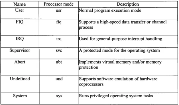
3.2 Processor Modes, Registers and PSRs (Program Status Register)
ARIvI processor has seven processor modes (User mode, fIQ mode, IRQ mode, $upervisor mode, Abort mode, Undefined mode, System mode). Every processor mode has different banked general register group. Also there is a CPSR (Current Program Status Register) and a SPSR (Saved Program Status Register) except system mode and user mode (there is no SPSR for system mode and user mode).
Processor modes:
ARM supports five types of exceptions, and a priviieged processing mode for each type. The five types of exceptions are:
1. Fast interrupt 2. Normal interrupt
3. Memory aborts, which can be used to impiement memory protection or virtuai memory
4. Attempted execution of an undefined instruction
5. Software interrupt (SWI) instructions which can be used to make a caTi to an operating system.
When an exception occurs, some of the standard registers are replaced with registers specific to the exception mode. Ail exception modes have replacement banked registers for Ri 3 and Ri 4. The fast interrupt mode has more registers for fast interrupt processing.
When an exception handier is entered, Ri4 holds the retum address for exception processing. This is used to retum afier the exception is processed and to address the instruction that caused the exception.
Register Ri3 is banked across exception modes to provide each exception handier with a private stack pointer. The fast interrupt mode aiso banks registers R$ to R12 SO that
14
There is a sixth privileged processing mode, System mode, which uses the User mode registers. This is used to nin tasks that require priviieged access to memory andlor coprocessors, without limitations on which exceptions can occur during task.
Ail the processor modes are described in Table 3.1
Table 3-1: Processor mode description
Name Processor mode Description
User usr ‘Tormal program execution mode
FIQ fiq Supports a high-speed data transfer or channel
wocess
IRQ irq Jsed for general-purpose interrupt handiing
Supervisor svc \.protected mode for the operating system
Abort abt Implements virtual memory andlor memory
)rotection
Undefined und Supports software emulation of hardware
coprocessors
System sys uns privileged operating system tasks
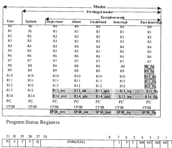
Registers:
The ARM has 15 user-accessible general-purpose registers called RO to R14 and a current program status register (CPSR) and a program counter R15.
The ARM processor has a total of 37 registers:
• 31 general-purpose registers, including a program counter. • 6 status registers.
These registers are 32 bits wide. Registers are arranged in partially overlapping banks, with a different register bank for each processor mode. At any time, 15 general-purpose registers (RO-R14), one or two status registers and the program counter are visible.
The general-purpose registers RO-R15 can be split into three groups. These groups differ in the way they are banked and in their special-purpose uses:
• The unbanked registers RO-R7 • The banked registers R8-R14 • R15 is the PC (Program Counter)
Banked register means physical address of the register depends on processor mode. Unbanked register means physical address of the register doesn’t depend on processor mode.
Tite unbaitked registers RO-R 7:
Each ofthem refers to thesame 32-bit physical register in ail processor modes. They are completely general-purpose registers, with no special uses implied by the architecture, and can be used wherever an instruction allows a general-purpose register to be specified.
The banked registers R8-R14:
The physical register referred to by each of them depends on the current processor mode. Where a particular physical register is intended, without depending on the current processor mode, a more specific name is used. Almost ail instructions allow the banked registers to be used wherever a general-purpose register is allowed.
R15 is tue PC (Program Counter):
When an instruction reads Ri 5, the value read is the address of the instruction plus $ bytes. Ail the registers are described in Table 3.2.
PSRs (Program Status Registers):
The current program status register (CPSR) is accessible in ail processor modes. It contains condition code flags, interrupt disable bits, the current processor mode, and other status and control information. Each exception mode aiso has a saved program status register (SPSR) that is used to preserve the value of the CPSR when the associated
16
exception occurs. User mode and System mode do flot have an SPSR, because they are not exception modes.
Table 3-2: Registers [261
IVIo des
Rl4svc Rl4abt R14 tRi3 irq!.i,. RItiq
PU PC
3PSR SRmbt SPSRwid SP_frq.45 SPSR_fii
Program Status Registers
3! 30 29 28 27 26
DNM(RAZ)
$
I f T M4 M3 M2 MI M
The condition code flags in PSR:
The N, Z, C, V (Negative, Zero, Carry and overflow) bits are coÏlectively known as the
condition code flags. The condition code flags in the CPSR can be tested by rnost instructions to determine whether the instrtiction is to be executed.
The condition code flags are usually modified by:
• Execution ofa comparison instrtlction (CMN, CMP, TEQ, TST).
• Execution of some other arithrnetic, logical or move instruction, where the
destination register of the instruction is flot RI5. Most of these instructions have both a flag-preserving and a flag-setting variant, with the latter being selected by
— .“.,, .-.“..,“‘-.,
_______________________________
Exception mok
User System [uIwrisot Abort Undelined Interrup( Fast Intern
RU RU RU RU RU RU RU RI RI RI RI RI RI RI R2 R2 R2 R2 R2 R2 R2 R3 R3 R3 R3 R3 R3 R3 R4 R4 R4 R4 R4 R4 R4 R5 R5 R5 R5 R5 R5 R5 R6 R6 R6 R6 R6 R6 R6 R] R7 R7 R] R? R7 R7 R8 R$ R8 Rb Rh R8 .8fi4 R9 R9 R9 R9 R9 R9 fi
RIO RIO RIO RIO RIO RIO
RI I R.II RI I RI I RI I RIl
RI2 RI2 R12 RI2 R12 RI2 i”fi
R 13 R13 13svc R13alt j RI3Zirg4
R!4 R14
__________ ___________
PC PC PC PC PC
adding an S qualifier to the instruction mnemonic. Some of these instructions only have a flag-preserving version.
N: is set to bit 31 ofthe resuit ofthe instruction. Z: is set to 1 if the resuit of the instruction is O.
C: is set in one of four ways:
• For an addition, including the comparison instruction CMN (CoMpare Negative), C is set to 1 if the addition produced a carry (that is, an unsigned overflow), and to O otherwise.
• For a subtraction, C is set to O if the subtraction produced a borrow (that is , an
unsigned underflow), and to 1 otherwise.
• For non-additionlsubtractions that incorporate a shift operation, C is set to the Ïast bit shified out ofthe register by the shifier.
• For other non-additionlsubtractions, C is left unchanged.
V: is set in one oftwo ways:
• For an addition or subtraction, V is set to I if signed overflow occurred. • for non-additionlsubtraction, V is normally lefi unchanged.
The condition flags can be modified in these additional ways:
• Execution of an MSR (Move to PSR from general-purpose Register) instruction, as part ofits function ofwriting a new value to the CPSR or SPSR.
• Execution of MRC (Move to ARM Register from Coprocessor) instructions with destination register R15. The purpose of such instructions is to transfer coprocessor-generated condition code flag values to the ARM processor.
• Execution of some variants of the LDM instruction. These variants copy the SPSR to the CPSR, and their main intended use is for retuming from exceptions. • Execution of flag-setting variants of arithmetic and logical instructions whose
destination register is R15. These also copy the SPSR to the CPSR, and are mainly intended for retuming from exceptions.
The controtflags in PSR are:
• I: Disables 1RQ interrupts when it is set. • f: Disables fIQ interrupts when it is set. • T: O (ARM execution), 1 (Thumb execution)
• Mode bits: M4...M0: Processor Mode. 0x10 (User), 0x11 (fIQ), 0x12 (IRQ), 0x13 (Supervisor), 0x17 (Abort), Oxlb (Undefined), Oxlf(System).
Other bits in the Program Status Registers are reserved for future expansion. The format of PSR is described in table 3.2.
3.3 ARM
instructions
ARIVI instructions are 32 bit fixed-length RISC instruction set. figure 3.1 shows the ARM architecture version 5 instruction set encoding.
figure 3.2 shows multiplies and extra ioadlstore instructions figure 3.3 shows miscellaneous instructions
Almost ail instructions can be conditionally executed; which means that they only have their normal effect on the programmer’ s model state, memory and coprocessors if the N, Z, C and V flags in the CPSR satisfy a condition specified in the instruction. If the flags do flot satisfy this condition, the instruction acts as a NOP. Table 3.3 shows the condition code encoding.
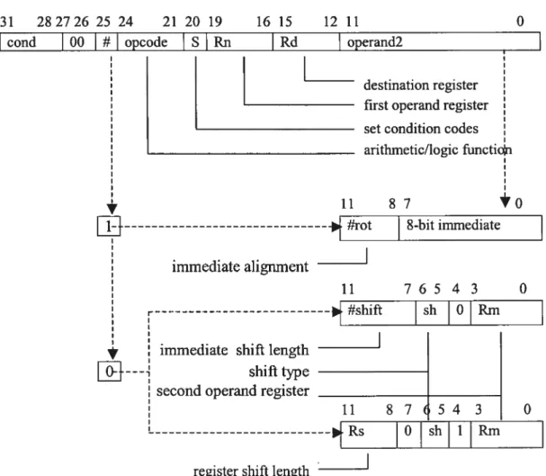
31302928272625 24 23 22 21 201912171615141312 11 10 9 8 7 6 5 4 3 2 1 0 Data processing immediate
shift Miscellancous instructions: See figure 3-3 Data processing register shift Miscellaneous instructions: See figure3-3
Multiplies, extra loadlstores: Scefigure3-2 Data processing llnmedate Undefmed instruction Move immediate to status register LoaWstore immediate offset Loadlstore register offset Undefined instruction Undefined instruction Loadlstore multiple Undeflned instructions Branch and branch with link Branch and branch wiffi Iink Andchange to thumb Coprocessor Ioad!storeand double Register transfers Coprocessor data processing Coprocessor register transfers Software interrupt Undefmed instruction
cond 000 opcode S Rit Rd Shifi amount shifi Rm
cond 000 lOxx O xxxxxxxxxxxxxxx O xxxx
cond 000 opcode S Ru Rd Rs O shift 1 Rrn
cond 000 lOxx O xxxxxxxxxxxx O xx 1 xxxx
cond 000 xxxxxxxxxxxxxxxxx 1 xx 1 xxxx
cond 001 opcode S Rn Rd rotate immediate
cond 001 10 x 00 xxxxxxxxxxxxxxxxxxxx
cond 001 10 R 10 rnask SBO rotate inunediate
cond 010 P U B W L Rn Rd immediate
cond 011 P U B W L] Rn Rd Shifi amount shifi O Rrn
cond 011 xxxxxxxxxxxxxxxxxxxx 1 mx
1 111 0 xxxxxxxxxxxxxxxxxxxxxxxxxxx
cond 100 P U S W L Rn Register list
1111 100 xxxxxxxxxxxxxxxxxxxxxxxxx
cond 101 L 24-bit offset
1111 101 H 24-bit offset
cond 110 P U N W L Ru CRd cp-nurn 8-bit offset
cond 1110 opcodel CRn CRd cp-num opcod2 O CRin
cond 1110 opcodel L CRu CRd cp-num opcod2 1 CRin
cond 1111 swinumber
1111 1111 mooooœocxoocx
20
Multiply (accumulate)
_______ ___________ ________ ________ ___________
Multiply (accumulate) long Swap/swap byte Loadlstore halfword Register offset Loadlstore halfword Immediate offset Loadlstore two words register offset Load signed halfwordlbytc Register offset Loadlstore two words immediate offset Load signed halfwordlbyte Immediate offset
Figure 3.2: Multiplies and extra loadlstore instructions [26]
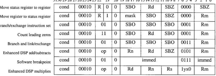
Move status register to register Move register to status register Brmchlexchange instruction set Count leading zeros Branch and Iinklexchange Enhanced DSP addlsubtracts Software breakpoint Enhanced DSP multiplies
3130292827262524 23 22 21 20191817161514131211 109 8 76 5 43210
cond 0000 00 A S Rd Rn Rs 1001 Rm
cond 0000 1 U A S RdHi RdLo Rs 1001 Rm
cond 0001 0 B 00 Rn RU SBZ 1001 Rm
cond 000 P U O W L Rn RU SBZ 1011 Rm
cond 000 P U T W L Rn RU HiOffset 1011 LoOffset
cond 000 P U O W O Rn RU SBZ i i S 1 Rm
cond 000 P U O W 1 Rn RU SBZ 1 1 H 1 Rm
cond 000 P U 1
w o
Rn RU HiOffset 1 1 5 1 LoOffsetconU 000 P U 1 W 1 Rn RU HiOffset 1 1 H 1 LoOffset
31302928272625242322 21 20 19 18 17 16 15 1413 12 111098 7 6 5 4 3 2 1 0
conU 00010 R O O SBO RU SBZ 0000 SBZ
conU 00010 R 1 0 mask SBO SBZ 0000 Rm
conU 00010 01 0 SBO SBO SBO 0001 Rm
conU 00010 11 0 SBO RU SBO 0001 Rm
cond 00010 01 0 SBO SBO SBO 0011 Rm
cond 00010 op O Rn RU SBZ 0101 Rm
cond 00010 01 0 immed 0111 immed
cond 00010 op O RU Rn Rs lyxO Rm
Table 3-3: Condition code encoding 1261
Opcode Mnemonic Meaning Condition flag state
1R3128 extension
0000 EQ Equal Z set
0001 NE Not equal Z clear
0010 CS/HS Carry Set/unsigned C set
Higher or Same
0011 CC/LO Carry Clear/unsigned C clear
LOwer
0100 MI Mlnus/negative N set
0101 PL PLus/positive or zero N clear
oiio
vs
Overflow V set0111 VC No overflow V clear
1000 HI Unsigned higher C set and Z clear
1001 ES Unsigned lower or C clear or Z set
same
1010 GE Signed Greater than or (NV)
Equal
1011 LT SignedLessThan (N !V)
1100 GT Signed Greater Than Z0 or N!V
1101 LE Signed Less than or Z1 or N!V
Equal 1110 AL ALways (unconditional) 1111 N’! Dependson architecture version
3.4 Addressing Modes
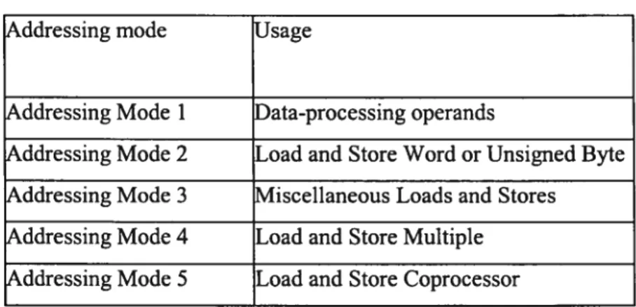
ARIVI Instructions have 5 kinds of addressing modes. Different addressing mode is used
22
Table 3-4: Addressing mode
ddressing mode Jsage
ddressing Mode 1 )ata-processing operands
ddressing Mode 2 Load and Store Word or Unsigned Byte ddressing Mode 3 vliscellaneous Loads and Stores ddressing Mode 4 Load and Store Multiple
ddressing Mode 5 Load and Store Coprocessor
The following is more detailed description:
Addressing Mode 1 (figure 3.4):
Addressing Mode 1 is used in Data-Processing instructions to generate the second operand (Shifier Operand). Shifier-Operand could be:
Tmmediate: shifter_operand=8-bit immediate Rotate_Right (#rot * 2)
if #rot=O then shifter_carry_out=C_flag else shifler_carry_out=shifier_operand[3 1]
(it is also the last bit shifted out of the value by the shifier, see figure 3.8)
Register: if .4=0, then shifter_operand=Rm shifler_carry_out=C_flag
Scaled Register: Rm is shifted by the amount ofRs or #shift.
The shifitype (table 3.5) can be: LSL (00), LSR (01), ASR (10), ROR (11), ROX (11) (R11.7=0).
23
Table 3-5: Shift types
Shift )escription
SL (figure 3.5) Logical Shift Left $R (figure 3.6) Logical Shift Right
SR (figure 3.7) \rithmetic Shift Right ROR (figure 3.8) Otate Right
ROX (figure 3.9) Otate right with eXtend
31 282726 25 24 21 20 19 16 15 12 11 0
cond 00 # opcode S Rn Rd operand2
I
destination register first operand register set condition codes anthmetic/logic functic V 11 87 - #rot immediate alignment
I
8-bit immediate 11 76543 0 sh 0Rm shift immediate shifi lengthI
I shifi type
second operand register
11 87 54 3 0
O sh 1 Rm
register shift length
Figure 3.4: Addressing mode 1 data processing instruction binary encoding j26J n
+0
24 LSL: LSR:
j
Ii
ASR: 31 30 ROR: Shifter-Cariy-Out=Rm[2 *rot... 1]Figure 3.8: ROR operation
f
1.
shifler-carry-out Figure 3.5: LSL operation O 3130 1 0 Figure 3.6: LSR operafion 31 30 I OFigure 3.7: ASR operation
n
H
ROX: ni n il . 10 Shifter-Carry-OutRm[0JAddressing Mode 2 (figure 3.10):
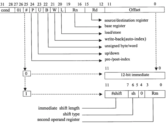
immediate shifi length shifi type second operand register
source/destination register base register loadJstore * write-back(auto-index) * unsigned byte/word * up/down * pre-/post-index
Figure 3.10: Addressing mode 2 Single word and unsigned byte transfer instruction binary encoding [26J
It is used in LoadlStore WordfUnsigned Byte instructions addressing.
The instructions are: LDR, LDRB, LDRBT, LDRT, STR, STRE, STRBT, STRT.
P and W combination decides the index mode: P=0: post-index
W=0: post index
W=1: LDRT, only post index P=1: pre-index and register offset
W=0: register offset 31 28272625 24 23 22 21 20 19 16 15 12 11 0 cond 01
J
PJ
Jj
LW L Rn Rd Offset y 11 11 yO 12-bit immediate 7654 3 O W=1: pre-index26
Offset could be:
• Immediate offset: offset=12-bit immediate • Register offset: R11 .4=0 then offset=Rm
• Scaled register offset: Rm is shifted by the amount of#shift.
U is used to indicate Rn Plus (U=1) or Minus (U=0) the offset. B is used to indicate Unsigned Byte (B=1) or Word (B=0). L is Load (L=1) or Store (L=0) operation.
Addressing mode 3 (figure 3.11):
1615 12 11 $ 7 6 5 4 3 0 Rd offsetH 1 S H 1 offsetL source/destination register base register load/store write-back(auto-index) up/down pre/post-index 3 0 11 $ y imlTl74 imm3 11 $ 3O
oooo
[Rm offset registerFigure 3.11: Addressing mode 3 Half-word and signed byte transfer instruction binary encoding 1261
It is used in loadlstore half word, signed haif word signed byte and double word instructions. The instructions are: LDRH, STRH, LDRSH, LDRSB, LDRD, STRD.
31 2$ 27 2524 23 22 21 20 19
cond 000
U: Indicates whether the offset is added (U=1) to the base or subtracted (U=O) from the base.
L: Indicates Load (L=l) or Store (LrO) instruction.
S: It distinguishes Signed (5=1) or Unsigned (5=0) half-word access. H: Indicates Haif-word (H=1) or Byte (H=0) access.
Offset could be:
• Tmmediate offset: offset=(offsetH «4) or offsetL • Register offset: offset=Rm
Addressing mode 4 (figure 3.12):
It is used in loadlstore multiple instructions.
Load Multiple instructions load a subset (possibly ail) of the general-purpose registers from memory. Store Multiple instructions store a subset (possibly ail) of the general purpose registers to memory.
Load and Store Multiple addressing modes produce a sequential range of addresses. The lowest-numbered register is stored at the lowest memory address and the highest numbered register at the highest memory address.
The general instruction syntax is:
LDMISTM {<cond>} <addressing_mode> <Rn>, <registers>
addressing mode is one ofthe following 4 addressing modes:
• TA: P=0 U=1, Start address=Rn, Endaddress=Rn+4*N4
• lB: P=1 U=1, Start_address=Rn+4, End_address=Rn+4*N
• DA: P=0 U=0, Start address=Rn4*N+4, Endaddress=Rn
• DB: P=1 U=0, Start address=Rn4*N, Endaddress=Rn-4
28
P: O (include Rn) 1 (exciude Rn)
Rn: when W=1, change the base register Rn U=1: Rn is set to Rn+4*N
U=0: Rn is set to Rn4*N
L: Indicates Load (L=1) or Store (Lz=0) operate.
S: For LDMs that load the PC, the S bit indicates that the CPSR is ioaded from the SPSR. For LDMs that do flot load the PC and ail STMs, the S bit indicates that when the processor is a privileged mode, the User mode banked registers are transferred instead of the registers of the current mode.
31 2827 25 24 23 22 21 20 19 16 15 0
cond 100 PIUJ SjWJj. Rn register list
base register loadlstore
write-back(auto-index) restore PSR and force user bit up/down
pre/post-index
Figure 3.12: Addressing mode 4 Multiple register transfer instruction binary encoding 1261
Addressing modeS (figure 3.13):
It is used in loadlstore coprocessor instructions. LDC and SIC.
The combination of P and W is similar with addressing mode 2. U and L have the same meaning with addressing mode 2.
N: is coprocessor-dependent. Its recommended use is to distinguish between different sized values to be transferred.
29
31 2827 2524 23 22 21 20 19 16 15 12 11 8 7 0
cond
1100
PIUINIWILIRn
CRd CPn $-bitoffsetI
source/destination register base register
loa&store
write-back(auto-index)
data size(coprocessor dependant) up/down
pre/post-index
Figure 3.13: Addressing mode 5 Coprocessor data transfer instruction binary encoding 1261
3.5 Organization of the 5-stage ARM Pipeline
ARM architecture describes the processor’s instruction set and its interfaces with its closest memory resources. It includes version 3, version 4, version 5 and the latest architecture version 6. ARM micro-architecture is the implementation of its architecture. Table 3-6 compares ARM architectural pipeline depth, it starts with ARM7 with three stages, ARM9 and StrongARivl with five stages, and XScale with seven stages, ends with ARM11, which now has an eight-stage pipeline. In this work, we construct an ARM micro-architecture simulator of StrongARM with 5 pipeline stages, which implements ARIvI instruction set version 5. The ARIVI processors that use a 5-stage pipeline and separate instruction and data memory are organized as figure 3. 14.
The 5 pipeline stages:
Iitstrttction Fetch: The instruction is fetched from memory and placed in the instruction pipeline.
Instruction Decode: The instruction is decoded and register operands read from the register file. There are three read ports in the register file. Ah the data processing instructions with register shift, short multiply instructions and long multiply instructions
30
without accumulation instructions have 3 source register operands, there are also other instructions that need 1 or 2 source register operands, so most ARM instructions can read ail the source operands in one cycle. Except SMLAL and UMLAL, they need 4 register operands. Adding a 4th port would be bigger for saving only one cycle rarely, so these 2 instructions need 2 cycles in this stage.
Execute: An operand is shifled and the ALU resuit generated. If the instruction is a load or store the memory address is computed in the ALU. If the instruction is LDM or STM and is the first cycle of LDM or STM executed in this stage, the start address and end address of the memory block is computed in the ALU, and address incremented in the following cycles.
Bufftr/data: Data memory is accessed if required; otherwise the ALU result is simply buffered for one dock cycle to allow the same pipeline ftow for ail instructions.
Table 3-6: Comparison of ARM architectureal pipeline depth
Pipeline Stages Micro-architecture
1 2 3 4 5 6 7
W—
Clock (MHz)Fetch Decode Execute (ARJvI7)
150
Fetch Decode ALU Cache WB (strongARM)
233
Fetch Issue Decode Execute Memory WB (ARM1O)
266-325
Fetchi fetch2 Decode Shifier Execute Exceptn WB (XScale)
733
planned 1000
fetchi fetch2 Decode Issue Shifier ALU SAT WB (ARM1 1)
350-500 estimate> 1000
Write-back: The resuits generated by the instruction are written back to the register file, including any data loaded from memory. For those load instructions and LDM instructions that have auto-index addressing need to change the base register Rn, also write back in this stage, so there are twowrite ports in the register file.
32 pc+4 B,BL mov PC subs pc ldr PC D stage 1D_EXE EXE stage EXE_MEM MEM stage MEM_WB next PC W stage ID W stage
Chapter 4 Implementation of the
AR1VI
core mode!
This chapter presents the way we implement the regular pipeline, advanced properties (data forwarding, interlock), branch, CPSR, SPSR and some special instructions.
4.1 Ail the Instructions operation in different stage (except IF)
Signal description:
Since the pipeline structure is flot described in the specification manual we are strongiy following the notation and methodoiogy described by Hennessy Patterson [24].
Pipeline Registers (showed in figure 3.14): The pipeline registers are labeled with the names of the stages they connect. For example, JFID is the pipeline register between 1F and D stage, the same as D_EXE, EXE_MEM and MEM_WB. The pipeline registers carry both data and control from one pipeline stage to the next. They hold values temporariiy between dock cycles. Any value needed on a later pipeline stage must be placed in such a register and copied from one pipeline register to the next, until it is no longer needed. We note the name of the temporary value ‘pipeline register name’ +‘‘ + ‘temporary name’. For example IR in IF_ID is IF_ID_IR. Ail these temporary values are transferred as signal in paraliel between pipeline stages, the calculation inside a stage is sequential. These temporary values in different pipeline registers are:
IFD: R (instruction)
DEXE: R
TYPE (type of instruction showed in figure 3.1, 3.2, 3.3)
OPERATE (showed in instruction column of instruction in table 4.1) CP$R (current program status)
SPSR (saved program status)
A (RnIMUL_Rn) (iilustrated in figure 3.14) Bb (RmIUMLALRdHi/$MLALRdHi)
C (Rs/Rd of store instnicitons/UMLALRdLo/SMLALRdLo)
IMM (Irnm1 2/Irnrn2O/1mm24)
34 EXE_MEM: R TYPE OPERATE CPSR SPSR
ALUOutput (output of data processing instructions/UMLAL_RdHi /SMLALL_RdHi /address of loadlstore)
C (Rd of store instrucitons/Rm ofSWP and SWPB) D (changed base register value)
StartAddress (for LDM and STM) EndAddress (for LDMand STM)
Change_Base (indicate if the base register is to be changed) MEMWB:
TYPE OPERATE CPSR
ALUOutput
LMD (data read from memory) D
Change_Base
Table 4.1 shows ail the instructions operation in different stage (except 1F). Table 4.2 summanzes the work of eveiy stage.
Table 4-1: All the instructions operation in different stage
nstmction type Instruction ID EXE MEM WB )ata processing -Rn LUOutputE-A func LUOutput(-ALUOutput d immediate shift 3bE-Rm operand2 (except cmn, cmp, LUOutput
tst, teq), operand2 is showed in figure 3.4 addressing
nstmctiontype nstruction ID EXE v1EM WB
)ata processing ‘E—Rn egister shift Bb(-Rm
C-Rs )ata processing \E-Rn
immediate
vliscellaneous VIRS * \LUOutputE-PSR LUOutputE- ALUOutput
instructions1 LUOutput
,ISR 3bE-Rm SRE-Bb * *
‘Iove immediate vISR * SRE-operand2 (operand2 * *
o status register is showed in figure3.4
addressing mode 1)
Vliscellaneous X 3b<-Rm 3ranch to Bb, change CPSR * * instructions2
LZ bE-Rm \LUOutput(- number of‘O’ LUOutputE- ALUOutput Rd
)its before the first‘1’ inBb LUOutput
3LX2 b(-Rm LUOutput(-PC+4, branch ... LRE
o Bb, changeCPSR LUOutput
3KPT * LUOutputE-PC+4, write ... LR4
SPSR, CPSR change mode, .LUOutput
I bit, T bit(showed in table 3.2), and branch
4u1tip1ies extra vIUL 3bE-Rm C-Rs LUOutputÉBb*C ... vRJL_Rd
Ioad store vlore detailedin4.5.4 LUOutput
VILA \E-MULRn \LUOutput(A+Bb*C ... vIUL_Rd
3bE-Rm C-Rs vlore detailed in 4.5.4 \LUOutput ]MULL 3bE-Rm C-Rs LUOutputE(Bb*C)6332 \LUOutput- ALUOutput dHiE
)((Bb*C)310 )E-D LUOutput RdLoE-D vlore detailed in 4.5.4
SMULL 3b(-Rm C-Rs \LUOutput((Bb*C)6332 ... dHi
)E(Bb*C)310 LUOutput
dLo&D
Vlore detailed in 4.5.4
JMLAL 3b-Rm(1) )6C(2)+[Bb(1)*C(1)]30 ... dHi
C-Rs(1) LUOutput
3b-RdHi(2) LUOutput&Bb(2)+[Bb( 1) dLo(-D
CRdLo(2) *C(1)] + carry for
calculatingD
36
nstruction type nstruction ID EXE vIEM WB SMLAL Bb-Rm(1) D-C(2)+[Bb( 1)*C(1)J310 ... RdHi
C-Rs(1) LUOutput
BbE-RdHi(2) LUOutputE-Bb(2)+{Bb( 1) dLoE-D C-RdLo(2) *C(1)] +carry for
calculating D
Vlore detailed in 4.5.5
SWP &E-Rn LUOutputE-A CE-Bb LMD-mem[ALUOutput] dE- LMD
3bf-Rm Vlore detailed in 4.5.3 nem[ALUOutput]E-C
SWPB •.. ... LMD(-mem{AlUOutput]70 dE-LMD
iiem[ALUOutput] -Rm7•0
DRH(R) ±Rn LUOutputE-offset LMD E-mem[ALUOutput]15.0 tdE-LMD
bE-Rm (showed in figure 3.11 DE-D .nE-D
Lddressing mode 3), )-changed base
DRH(I) E-Rn ... ... dE-LMD
nE-D
STRH(R) E-Rn ... nem[ALUOutputj E-C15 O
bE-Rm DE-C )E-D
CE-Rd
STRH(I) E-Rn CE-Rd ... ... nE-D
DE-C
WRSB(R) E-Rn ... LML*mem[ALUOutputj7o dE-LMD
3bE-Rm signed extend; DE-D nE-D
CDRSH(R) E-Rn ... LMD-mem[ALUOutputJ15o dE-LMD
3bE-Rm signed extend; DE-D nE—D
DRSB(I) E-Rn ... LMD(-mem[ALUOutputj7o dE-LMD
signed extend; DE-D
DRSH(I) E-Rn ... LMD&mem[ALUOutput]iso UE-LMD
signed extend; DE-D
oad store LDR(I) E-Rn LUOutput(-offset LMD-mem[ALUOutput] d-LMD
immediate offset showed in figure 3.10 )E-D .irE-D
addressingmode 2),
)E-changed base
STR(I) E-Rn CE-Rd ... nem[ALUOutput](-C; DE-D RnE-D
Cf-C
Load store registe LDR(R) -Rn ... LMD-mem[ALUOutput]; RdLMD
)ffset 3bE-Rm )E-D
STR(R) E-Rn ... nem[ALUOutput](-C; DE-D RnE-D
BbE-Rm Cf-C CE-Rd
nstruction type Instruction ID EXE MEM WB oad store ZDM \±Rn Calaulate Startaddress LMD(-mem[Startaddress]; iELMD
nultiple end_address (showed in )E-D nD
figure 3.12 addressing mode [) D-changed base vlore detailed in4.5.1
STM ... ... nem[Start addressj E-Ri
DE-D More detailed in 4.5.2
3ranch and 3 * 3ranch to PC+(Imm«2) * *
)ranch withlink Immis the lower 24 bits
3L * LUOutputE-PC+4 branch \LUOutputE- ALUOutput LRE
o PC+(Imm«2), Immis LUOutput
the same as B instruction
3ranch and 3LX1 * t\LUOutput(-PC+4 change
... LRE
,ranch withlink f bit of CPSR (showed in \LUûutput
md change to able 3.2), branch to
humb >C+(Imm«2)+(H«1),
Immisthesame as B instruction, H is bit 24 ofiR
oprocessor load DC 10 10 [0 10
tore and double egister transfers STC 10 10 10 [0 Doprocessor data CDP 10 10 10 10 rocessing Doprocessor vICR 10 10 10 10 egister transfers vIRC 10 10 no 10
Software intemiptSWI LUOutputE—PC+4 save LUOutput(—ALUOutput LRE
SPSRchange CPSR Ibit \iUOutput
f_bitprocessor mode (showed in table 3.2),
)ranch
Notes:
• *: Nothing to do in that stage.
• ...: It does the same work with last instruction operation.
• (1): is the first cycle. • (2): is the second cycle.
3
• mem[addr]: is memory data in address ‘addr’ Table 4-2: Work of every stage
Stage Any instruction
Arithmetic_instruction j_Loadlstore instruction Branch_instruction
1F IfEXEchangePC then PC-EXENPC;
Else if MEM_changePC then PC —MEM NPC (hranch related signal showed in figure 4.5); Else PCE-PCO (PCO is used only in 1F stage to identify the address ofnext instruction);
IF ID IR -rnem[PC];
PCO E-PC+4;
Reg[ 15] (-PC+8;
ID ID EXE IR E-If ID IR;
IDEXETYPEE- decode type of instruction (table 3.1 3.2 3.3);
IDFXEOPERATE- decode operate of instruction (table 3.4 instruction narne); ID_EXE_PC E-Regs[ 15];
ID_EXE_A(-Regs[Rnj;
If (instruction is UMLAL or SMLAL) and (is 2’cycle ofrnultiply)thenID_E)Œ_Bb-Regs[RdHiJ
Else IQEXE_Bb E-Regs[Rm];
If (instruction is UMLAL or SMLAL) and (is 2 cycle of multiply) then ID_E)(E&E-Regs[RdLoJ Else if instruction is store then ID_E)Œ_&E-Regs[Rd]
Else IDEXEC-Regs[Rs];
If instruction is B, BL, BLX, SWI then ID EXE Irnrn-IMM24 (Iower 24 bits ofIR); Else if instruction is BKPT then ID EXE IrnrnE-1MM20 (lower 20 bits of IR); Else ID EXE ImrnE-IMM 12 (lower 12 bits of IR).
Stage Arithrnetic instruction Loadistore instruction Branch instruction
EXE EXE MEM 1RE-ID EXE 1R; EXE MEM iRE-ID EXE TR; EXE MEM iRE-ID EXE 1R;
EXE MEM TYPE- EXE MEM TYPE- EXEMEMTYPEE
1DEXETYPE; 1DEXETYPE; ID EXE TYPE,
EXEMEMOPERATEE- EXEMEMOPERATRE- EXEMEMOPERATE
-IDE)ŒOPERATE; IDEXEOPERATE; IDEXEOPERATE;
If destination register is PC E)Œ_MEM_ALUOutput(- EXE_NPCf (Rd’15) then address(A,Bb,C,Irnrn) (showed in IDE)ŒPC+Irnrn;
EXE_NPC-A func figure 3.10, 3.11 addressing mode
operand2(Bb,CJrnm) 2,3); EXE_changePCE- 1;
(showed in figure 3.4
addressing mode I); If change base register Rn then If instruction is BL, BLX. EXE_changePC E- 1; E)Œ_MEM_D E-changedbase; SWI, BKPT then
EXEMEMALUOutputE
MEMWBIRE EXEMEMIR; MEMWB TYPE -E)ŒMEMTYPE; MEMWBOPERATE< EXEMEMOPERATE; MEMWBALUOutput& EXEMEMALUOutput; MEMWBIR- EXEMEMIR; MEMWBTYPE
(-EXE MEM TYPE; MEMWBOPERATEE E)ŒMEMOPERATE;
If (instruction is Ioad) and destination register is PC (Rd15) then
MEMNPC
-rnern[E)ŒMEMALUOutputJ; Else if instruction is load then
MEMWBLMD E’ mem[E)ŒMEMALUOutputJ; Ef se if instruction is LDM then MEM_WBLMD( rnern[EXEMEMStartAddress] MEMWBStartAddress EXEMEMStartAddress+4; Else if instruction is store then
mem[EXEMEMALUOutputf= E)ŒMEMC;
Else if instruction is STM then
mem[EXEMEMStartAddressJ= EXEMEMC; StartAddress EXEMEMStartAddress±4; MEMWBEndAddress EXEMEMEndAddress; MEMWBD - E)ŒMEMD; MEM_WB_ChangeBase EXEMEMChangeBase (notify if
tEe base register is to be changed);
1finstructionis BL, BLX, SWI, BKPT then
MEMWBALUOutput EXEMEMALUOutput;
Stage Any instruction
Arithmeflc instruction LoadJstore instruction Branch instruction
EXE_MEMALUOuptutE- E)ŒMEMC(- IQEXE_C;
A func
operand2(Bb,Cjmm); If instruction is LDM STM then E)ŒMEMStaAddress Startaddress;
EXEMEMEndAddress Endaddress (showed in figure 3.12) addressing mode 4); MEM
WB Regs[RdJE- If instruction is LDM then If instruction is BL, BLX,
40
Stage Anyinstruction
Arithmeflcinstruction Load!store instruction Branchinstruction
Regs[LR]E
Ifinstructionis long rnultiply Else Regs[Rd]E- MEMWBLMD; MEMWBALUOutput.
Regs[RdHiJ
-MEMWBALUOutput; If changebase
Regs [RdLo]- Regs[Rnl- MEMWB_D.
MEMWBD;
Else ifinstructionis multiply then
Regs[RdMUL] E MEMWBALUOutput.
In short, more human readable form, each stage is doing the following: IF stage:
• Instruction fetch.
• Write PC+4 to PCO for next instruction address.
• Modify PC to PC+8, in order to be compatible with 3 stages pipeline. • Pass along values needed in the next stage.
ID stage:
• Decode ïnstruction to know its type and operate.
• Read PC for branch instruction to calculate the new address. • Read registers (3 register read ports).
• Extend sign ofimmediate (lower 24 bits or 20 bits or 12 bits ofthe instruction). • Pass along values needed in the next stage.
E)OE stage:
• Perform an ALU operation for data processing instructions. If the destination register is PC, sïgnal a branch.
• Calculate address for load/store instructions.
• Calculate the start address and end address of memory block forLDM1STM. • Calculate the new instruction address for branch instructions.
• Pass along values needed in the next stage.